Week 15: System Integration
Before starting
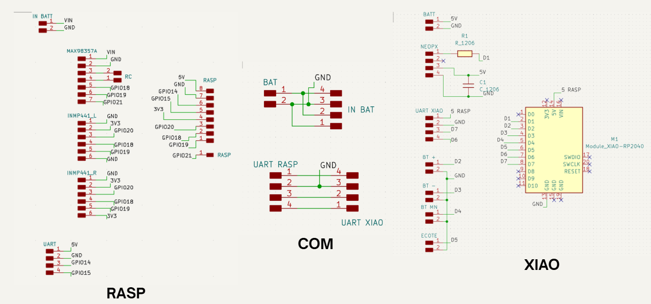
KINGER is an intelligent assistant. It integrates voice input, audio output and user controls sensing into a single cylindrical device. The system is built around a Raspberry Pi 5 as the main processing unit and a Seeed Studio XIAO ESP32-C6 as a dedicated coprocessor responsible for peripheral control and fast I/O handling.The physical form factor follows a cylindrical body with a rounded base that incorporates a self righting mechanism. All electronics are housed internally, and the device is powered through a combination of USB-C and a battery pack for 5V peripheral distribution.
System Planning
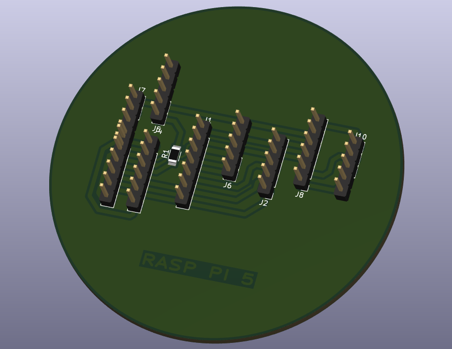
During the planning phase, the following components were selected based on availability, integration complexity, and compatibility with the Fab Lab manufacturing workflow:Raspberry Pi 5
Selected as the main processing unit. Handles audio processing, voice pipeline coordination, and system level logic. Connected via I2S for audio input and output, and UART for communication with the coprocessor.
Seeed Studio XIAO ESP32-C3
Selected as the peripheral coprocessor. Manages NeoPixel LED control, button inputs and low-latency I/O tasks. Communicates with the Raspberry Pi via UART at 115200 bps.
INMP441 I2S Microphone
Digital MEMS microphone selected for its I2S interface, which simplifies integration with the Raspberry Pi's digital audio bus. the unit is configured as a mono (left) for audio capture.
MAX98357A Audio Amplifier
Class D I2S amplifier selected for its direct digital audio input, high efficiency, and compact footprint. Drives a 3W 4Ω speaker directly from the Raspberry Pi's I2S output bus.
Speaker — 3W 4Ω
Downward facing speaker housed at the base of the enclosure. Audio exits through drilled holes in the base plate, projecting sound outward along the surface.
NeoPixel Ring (WS2812B — 16 LEDs)
Provides visual feedback for system state. Controlled by the XIAO ESP32-C6 via a single data line on GPIO2. Powered at 5V from the Raspberry Pi.
Physical Buttons (×4)
Three momentary buttons for Volume Up, Volume Down, action input and a extra button for a future. Wired to the XIAO ESP32-C6 digital inputs with 3.3V pull-up logic.
UART Communication
Serial communication at 115200 bps between Raspberry Pi GPIO14 (TX) → XIAO RX (D7) and Raspberry Pi GPIO15 (RX) → XIAO TX (D6). Enables command and feedback exchange between both processors.
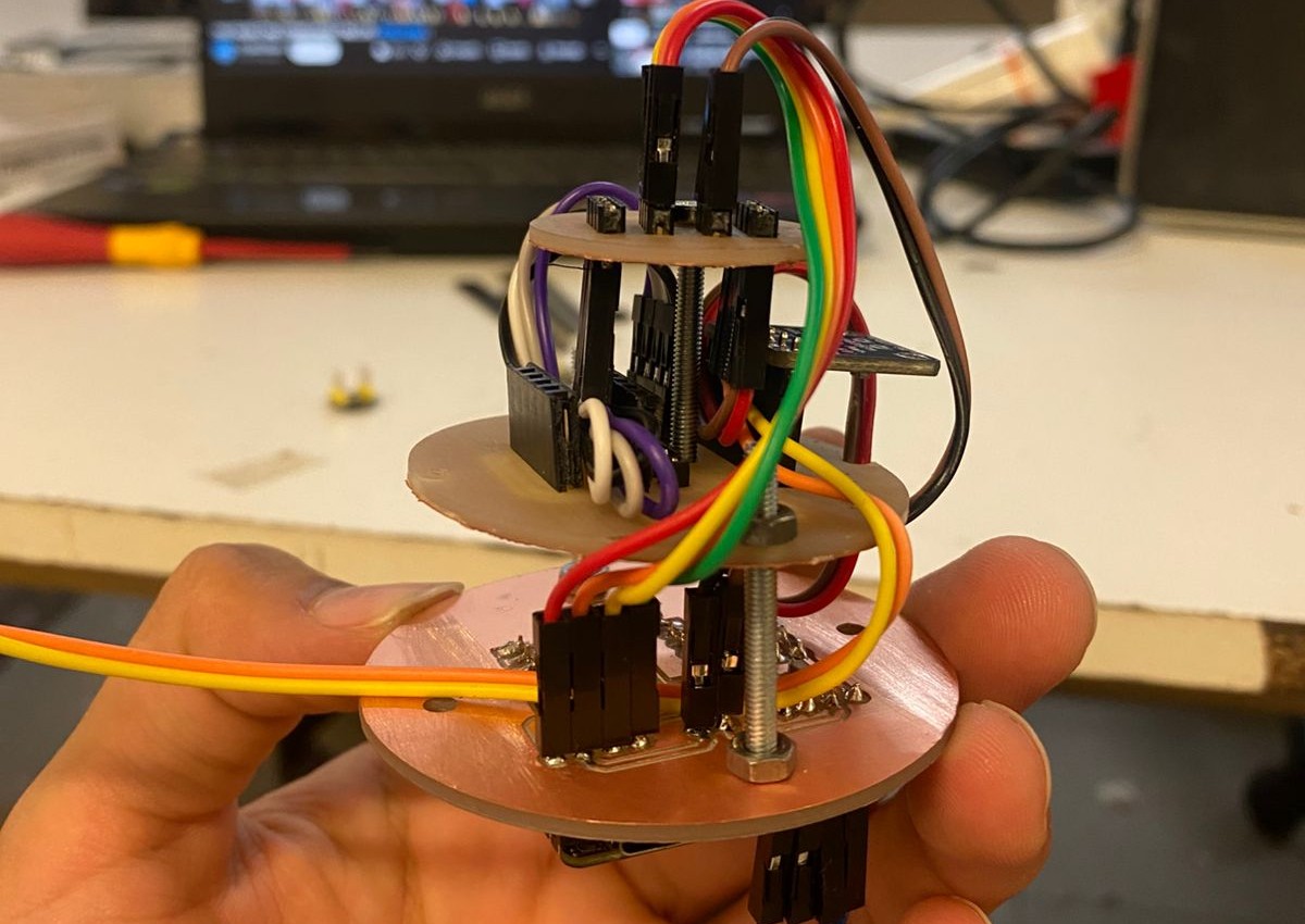
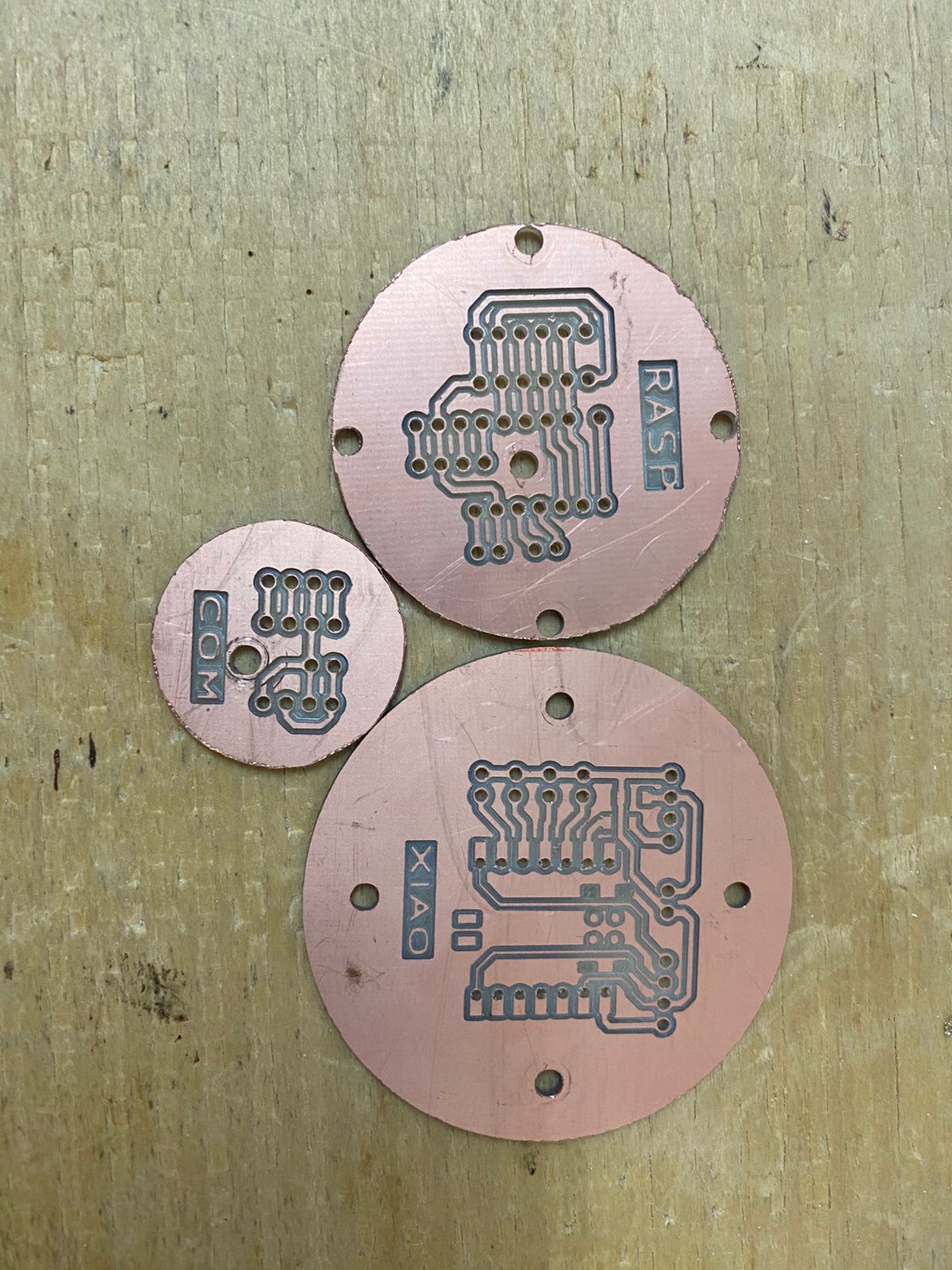
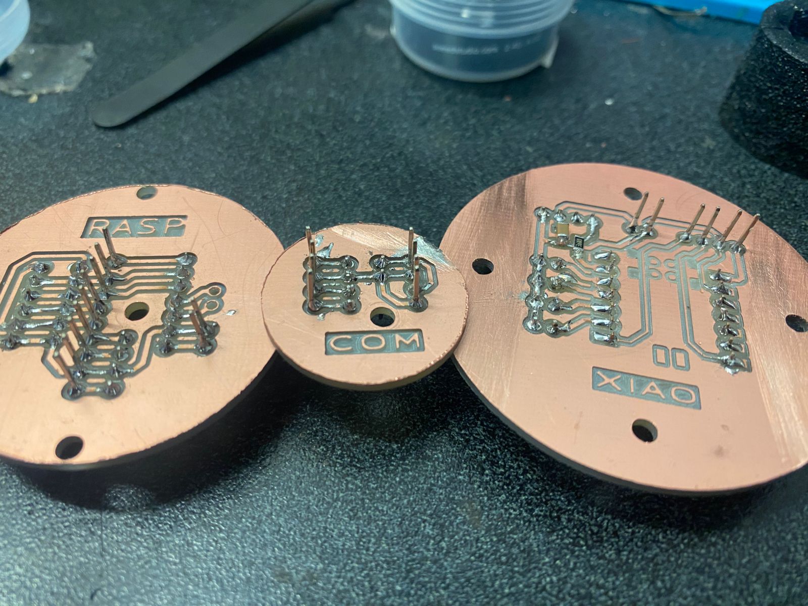
Custom PCBs
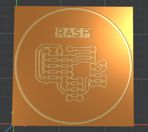
Three custom PCBs designed in KiCad and manufactured using the MonoFab SRM-20 milling machine. Designed as a stacked system to minimize internal volume.
PCB Strategy
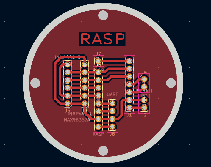
To minimize internal volume and simplify wiring, the electronic system was organized into three dedicated PCBs designed to be stacked vertically using spacers and screws. This approach centralizes all interconnections and reduces the number of flying wires inside the enclosure.PCB 1 — Raspberry Pi Interface Board
Top board in the stack. Contains the Raspberry Pi connector, I2S signal routing for both microphone input and amplifier output, UART signal lines, and power distribution connectors. Acts as the primary interface between the Raspberry Pi and the rest of the system.
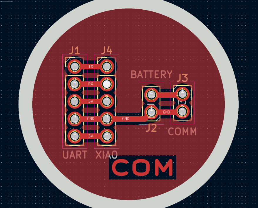
PCB 2 — Common Distribution Board
Middle board. Consolidates all common GND references, distributes the 5V and 3.3V rails to the other boards, and handles interconnection routing between PCB 1 and PCB 3. Eliminates redundant power traces and centralizes ground return paths.
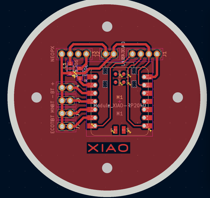
PCB 3 — XIAO Interface Board
Bottom board in the stack. Hosts the XIAO ESP32-C6 module and provides connection points for the NeoPixel data line, and button inputs. Receives power and UART signals from the distribution board above.
Architecture
Communication Architecture
The KINGER system is divided into two processing domains: the Raspberry Pi 5 handles all high level computation, and the XIAO ESP32-C6 manages real time peripheral control. Both devices share a common ground and communicate via UART.Raspberry Pi 5 — Main Processor
Responsible for all high level tasks: audio capture via I2S microphones, audio playback via the MAX98357A amplifier, voice processing pipeline coordination, and system level logic. Controls the MAX98357A directly over the I2S output bus and receives microphone data over the I2S input bus. Issues commands to the XIAO via UART.
XIAO ESP32-C6 — Coprocessor
Handles all peripheral I/O: NeoPixel LED ring control via WS2812B data protocol, and button state reading. Receives commands from the Raspberry Pi and returns peripheral feedback over the shared UART link.
UART Integration
Raspberry Pi TX (GPIO14) → XIAO RX (D7)
Commands and instructions are sent from the Raspberry Pi to the XIAO at 115200 bps. This includes LED control patterns, brightness levels, and other peripheral commands.
Raspberry Pi RX (GPIO15) → XIAO TX (D6)
The XIAO returns button states, and acknowledgment signals to the Raspberry Pi over this line.
Audio Input
The INMP441 digital microphone is connected to the Raspberry Pi's I2S input bus:- Left microphone: L/R pin tied to GND, configuring it as the left channel.
Audio Output
The MAX98357A amplifier receives audio data from the Raspberry Pi over the I2S output bus:- BCLK → GPIO BCLK (shared with microphone input clock)
- LRCLK → GPIO LRCLK
- DIN → GPIO DOUT
- VIN → 5V
- SPK+ and SPK− → 3W 4Ω speaker
User Interface Peripherals
- NeoPixel Ring: DATA line → XIAO GPIO2. Powered at 5V from the Raspberry Pi rail.
- Mute Switch (SPDT): → XIAO GPIO3, 3.3V logic.
- Action Button (Momentary): → XIAO GPIO4, 3.3V logic.
- System Status LED (optional): → XIAO GPIO5, 330Ω series resistor.
- Fan Control (optional): → XIAO GPIO6, via N-channel MOSFET, 5V.
Schematic
The following diagram shows the complete communication and power architecture of the KINGER system, including all connections between the Raspberry Pi 5, XIAO ESP32-C6, audio subsystem, and peripheral devices.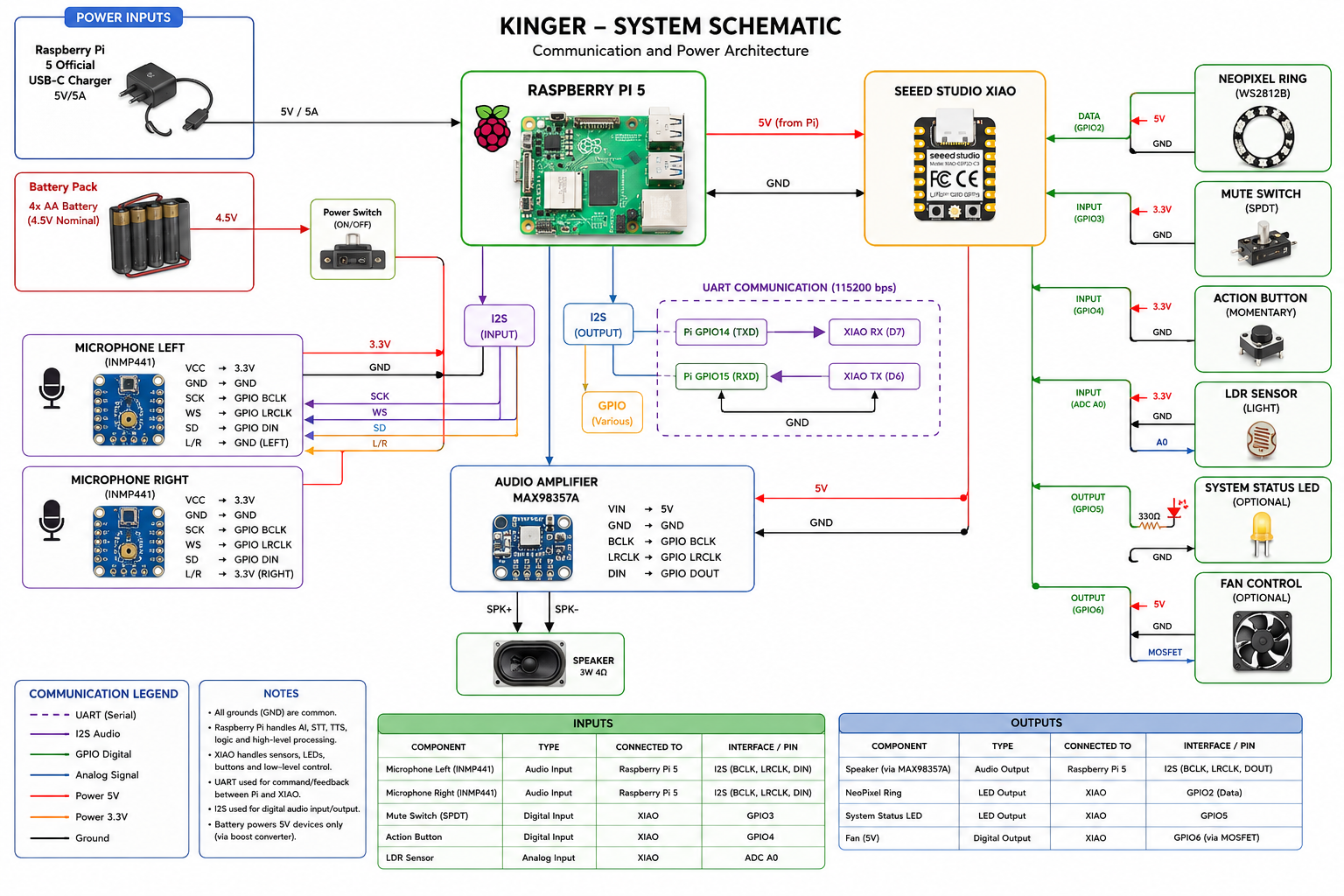
KINGER SYSTEM SCHEMATIC
The schematic above shows the full communication and power architecture. All GND references are common. The Raspberry Pi handles I2S audio input and output. The XIAO ESP32-C6 manages all peripheral I/O. UART links both processors at 115200 bps. Power is distributed from both the USB-C charger (Raspberry Pi) and a 5V and 3A battery pack (5V peripherals).
Electronic Design
Schematic Design
The KINGER schematic was designed in KiCad using the Fab Lab component library. Component selection was driven by interface compatibility: all audio components use I2S to keep the signal path entirely digital from microphone to amplifier. Power integration separates the Raspberry Pi supply (USB-C 5V/5A) from the peripheral battery rail, with a shared GND plane across the entire system.UART routing connects the Raspberry Pi's hardware serial pins (GPIO14/GPIO15) directly to the XIAO's D7/D6 pins. This avoids software serial implementations and ensures reliable communication at 115200 bps. All I2S lines — BCLK, LRCLK, DIN, and DOUT — are routed through PCB 1 to minimize signal path length between the Raspberry Pi header and the audio components.
PCB Layout
Component placement on each board was organized by functional domain. On PCB 1, the Raspberry Pi connector is centered and all I2S and UART signals radiate outward to their respective edge connectors. On PCB 3, the XIAO module is positioned centrally with all peripheral connectors on the perimeter for easy wiring to in enclosure components.Trace width and spacing were set to a minimum of 0.4 mm and 0.8mm across all boards to ensure reliable isolation during MonoFab milling. This value was determined based on previous manufacturing experience where narrower traces caused unintended shorts due to milling tool tolerances. Board dimensions were kept within the MonoFab SRM-20's working area.
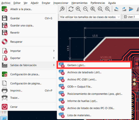
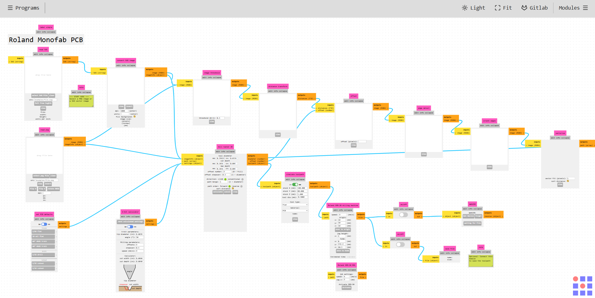
Manufacturing Preparation
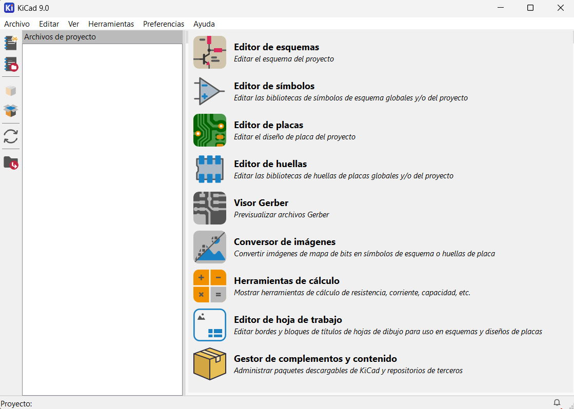
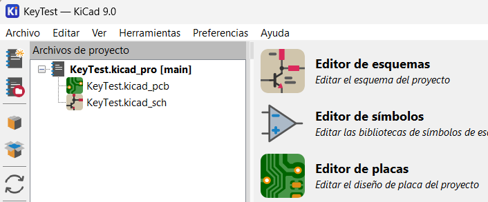
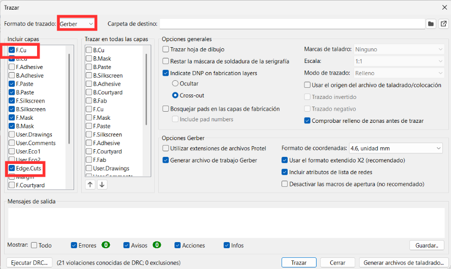
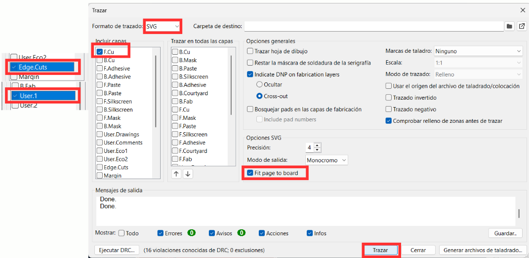
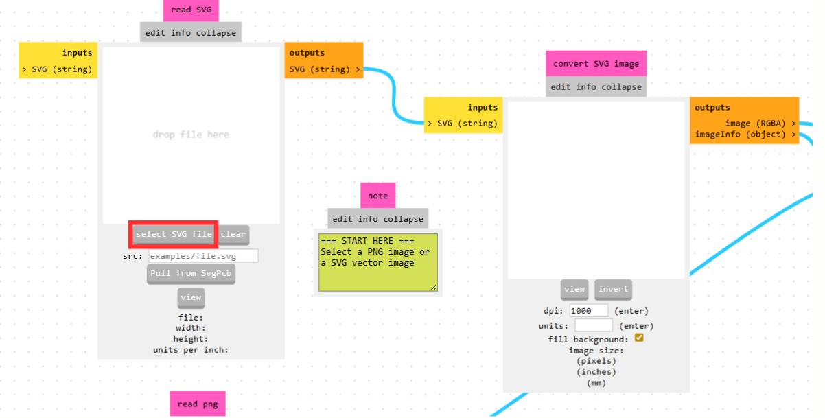
All three PCBs were manufactured using the MonoFab SRM-20 milling machine at the Fab Lab. Fabrication files were exported from KiCad as SVG files and processed through MODS CE to generate .rml toolpath files for drilling, trace milling, and board outline cutting. The complete KiCad design workflow, MODS toolpath generation, MonoFab operation, and soldering process are documented in the tabbed sections below.KiCad Main Interface
From this central project manager window, you can access the core tools:- Schematic Editor – Used to create and edit the electrical schematic of the project.
- Symbol Editor – Used to create or modify schematic symbols.
- PCB Editor – Used to design and route the printed circuit board layout.
- Footprint Editor – Used to create or modify PCB footprints.
- Gerber Viewer – Used to preview manufacturing Gerber files.
- Image Converter – Converts bitmap images into schematic symbols or PCB footprints.
- Calculator Tools – Provides electrical calculation utilities (resistors, trace width, etc.).
- Worksheet Editor – Used to edit drawing frames and title blocks.
- Plugin and Content Manager – Used to install additional libraries and third-party packages.
Creating a New Project
To create a new project, press Ctrl + N or go to the top menu → File → New Project, then choose the project name and save location. KiCad will automatically generate:- A project file (.kicad_pro)
- A schematic file (.kicad_sch)
- A PCB file (.kicad_pcb)
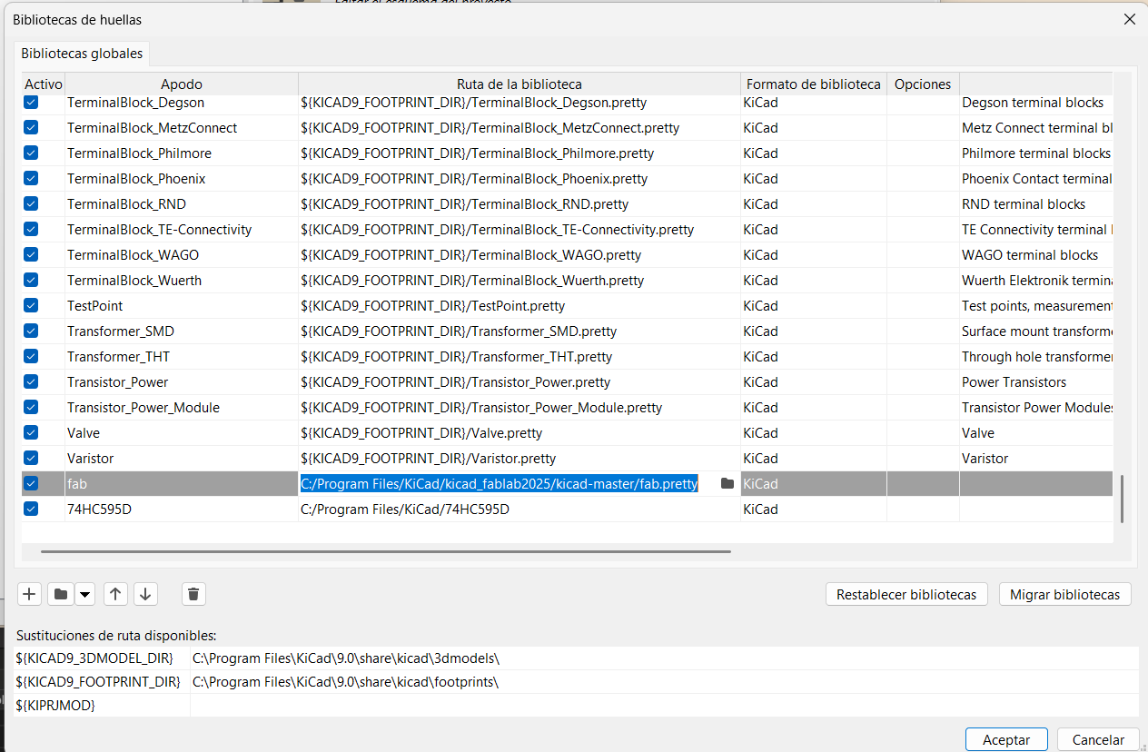
Adding a Library
You can download the FAB library by clicking on the dancing shrimp and:- Place the downloaded files in a chosen folder.
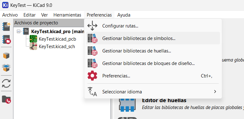
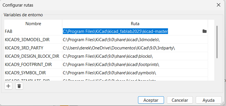
- Go to: Preferences → Configure Paths
Here you define the directory path where the library files are stored. This step ensures KiCad can locate external resources. - Importing Footprints
- Go to: Preferences → Manage Footprint Libraries
- Click "Add Existing Library"
- Select the folder containing the .pretty file and choose a name for the library.
Workspace
When we open the project in the Schematic Editor, we find an interface with a main menu and several toolbars surrounding the workspace. This is where electronic components are placed and connected using schematic symbols.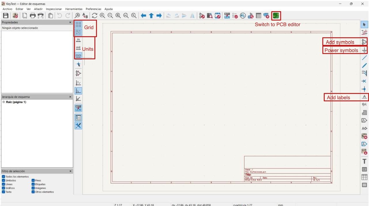
Adding a Component
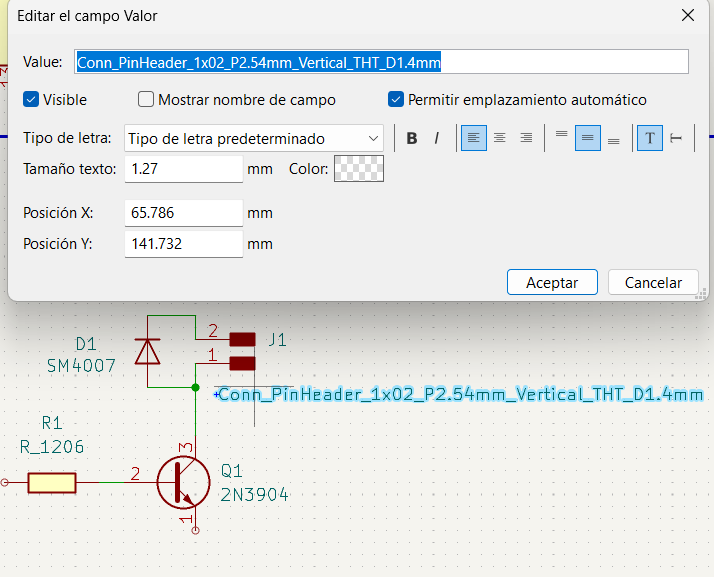
A shortcut to access the components menu is the A key. Once there, search for the component and choose the preferred package size. To modify its name and other parameters, double-click on it.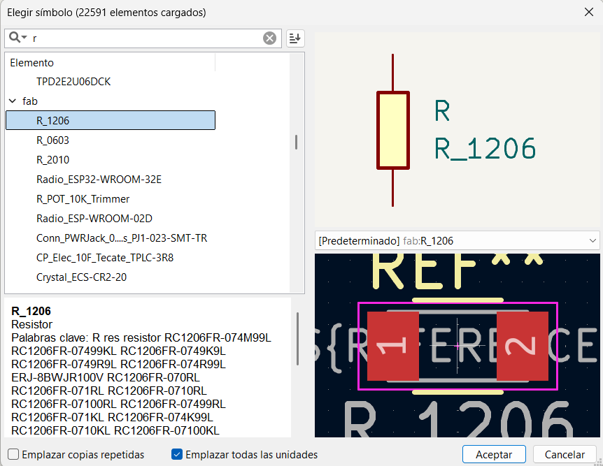
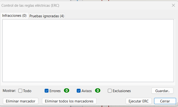
Electrical Rules Checker
Before switching to the PCB Editor, go to Inspect → Electrical Rules Checker (ERC). Running the ERC verifies the logical integrity of the schematic before generating the board layout. Intentionally unconnected pins will appear as errors but can be consciously dismissed after review.
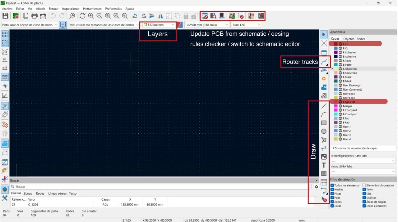
PCB Editor
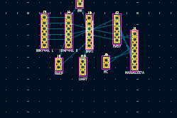
Once in the PCB Editor, select Update PCB from Schematic. This opens a window listing all schematic elements to be imported. After pressing OK, all components are placed on the board in an unordered state and must be manually arranged.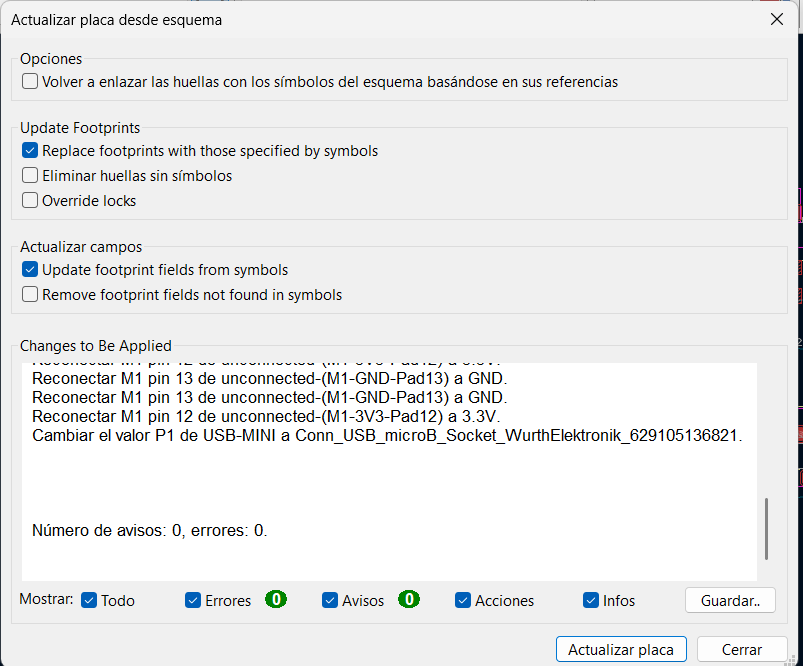
Important
Returning to the Schematic Editor to make changes is always possible. Whenever changes are made, select Update PCB from Schematic again in the PCB Editor to import the updated components.
Edge.Cuts
Once component placement is finalized, define the board outline by selecting the Edge.Cuts layer and drawing the boundary using the line tool. This layer defines the physical shape of the PCB and determines where the milling machine will cut the board free from the substrate.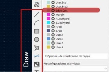
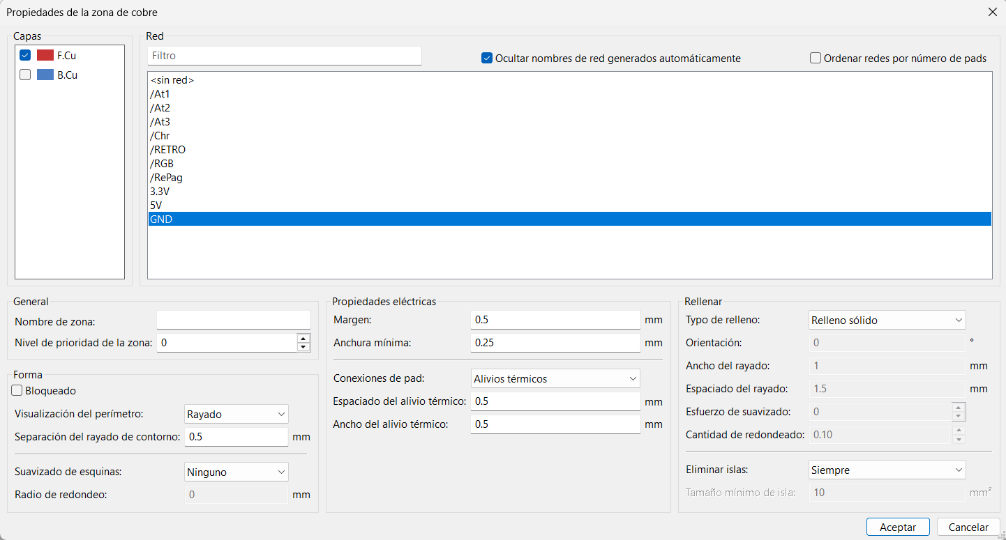
Copper Pour
For electrical reliability and manufacturing quality, a copper pour is added to the PCB. A copper pour fills a defined area with copper connected to a specific net, typically GND, serving several important purposes:- Improves electrical grounding by creating a low-impedance ground plane.
- Reduces electrical noise and electromagnetic interference.
- Enhances heat dissipation by spreading thermal energy across a larger surface.
- Reduces the number of routed traces required, simplifying layout.
- Optimizes manufacturing by balancing copper distribution on the board.
How to Add a Copper Pour
- Click on the Add Filled Zone icon in the right-side toolbar.
- Select the desired copper layer (F.Cu for the top layer or B.Cu for the bottom layer).
- Assign the zone to the GND net.
- Draw the polygon outline following the Edge.Cuts boundary.
- Close the polygon shape.
- Press the B key to fill the copper zone.
Important
Every time changes are made to the PCB — adding traces, moving components, modifying routing — press the B key again to refill and update the copper zone.


- Output format set to SVG for MonoFab compatibility.
- Each layer selected individually: traces, Edge.Cuts, and User layers.
- "Fit page to board" enabled to ensure correct scaling.
- Click "Plot" to generate the output files.
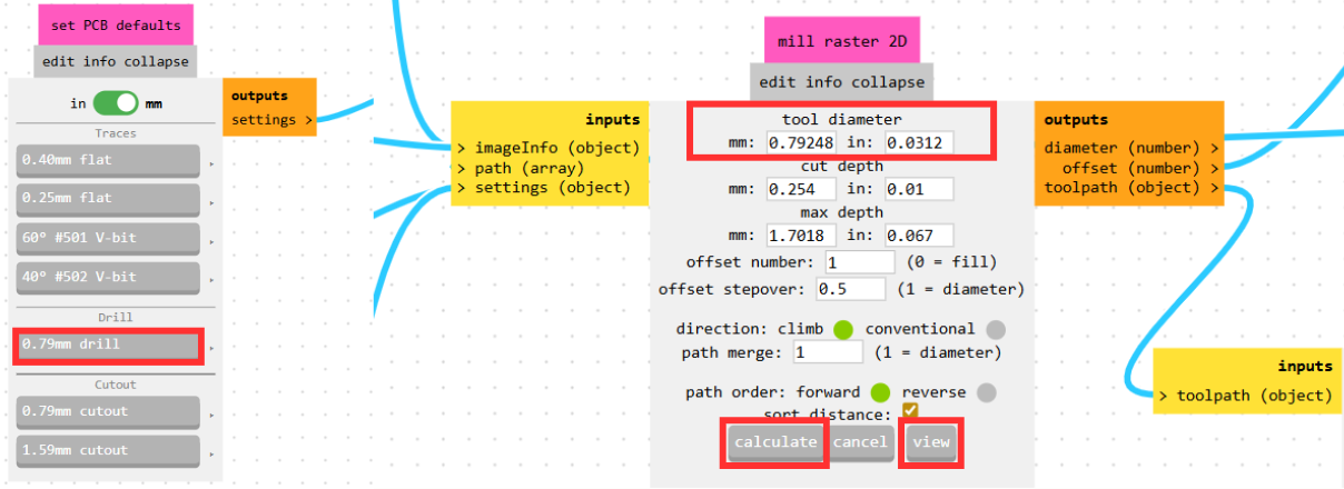
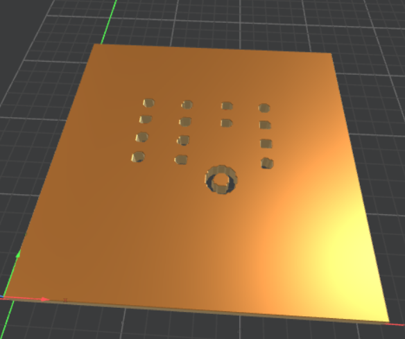
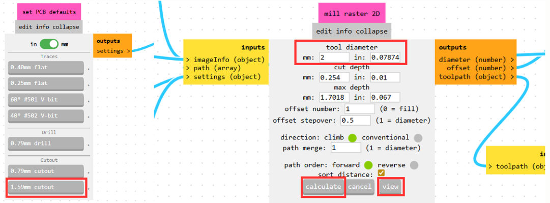
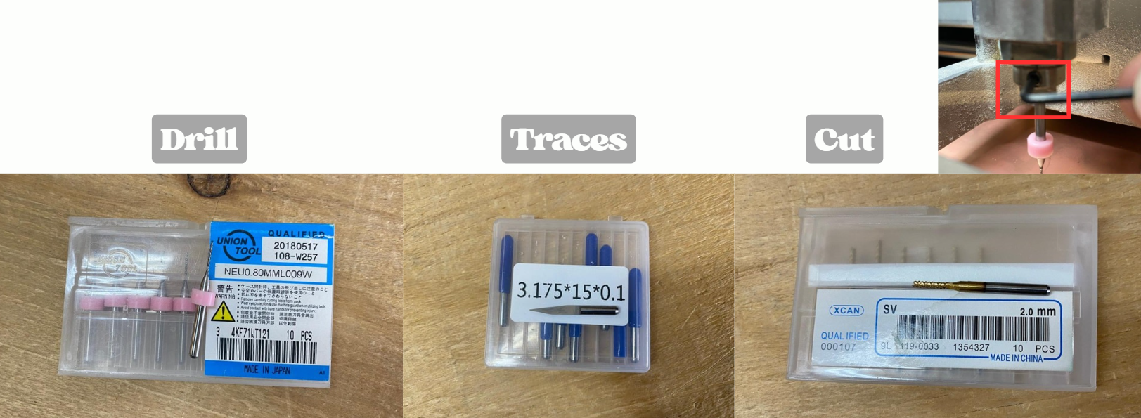
Drilling Process
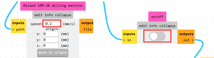
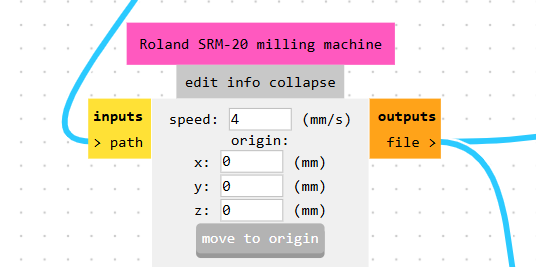
For drilling, a 0.79 mm drill bit is used. The feed rate in the Roland SRM-20 module is set to 0.2 mm/s to prevent tool breakage under the stress of plunge cuts.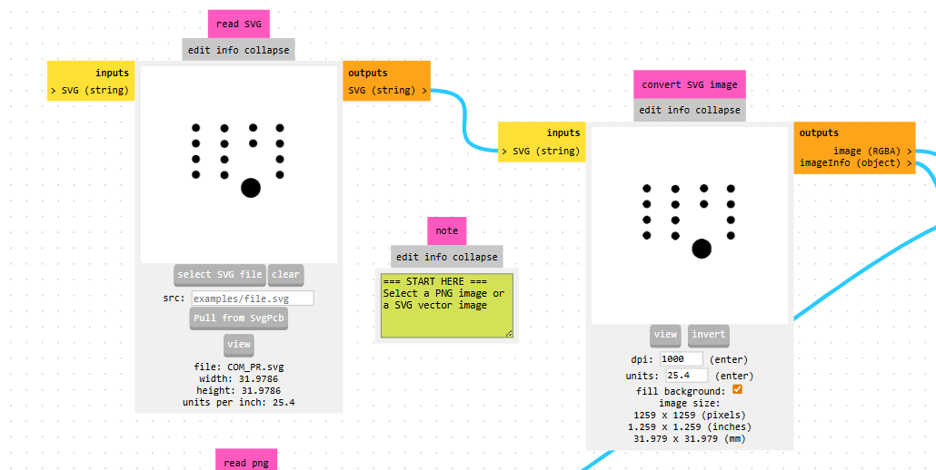
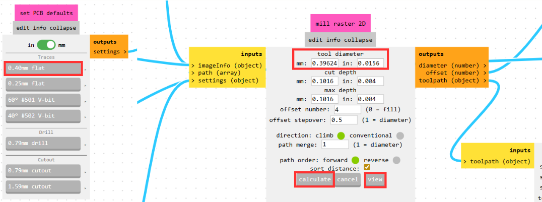
Traces Milling
The trace milling process follows the same setup as drilling, with one key difference. When the SVG is imported, copper traces may appear in black, indicating that the tool would remove them — this is incorrect.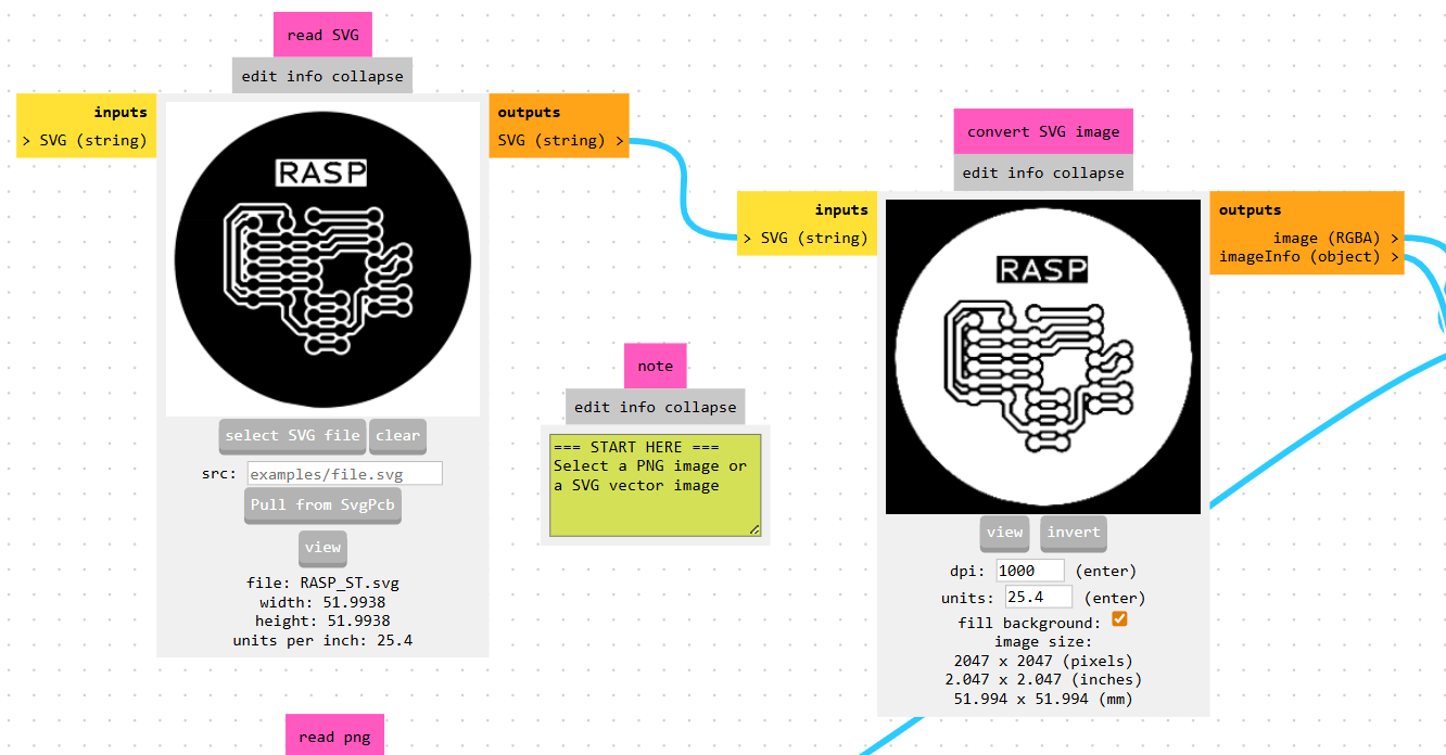
Board Outline
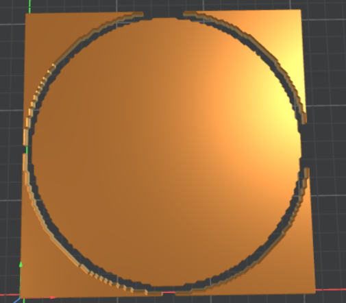
For cutting the board outline, a 1.59 mm cutout tool is used with a feed rate of 4 mm/s, maintaining the origin at (0,0,0).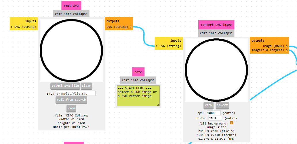
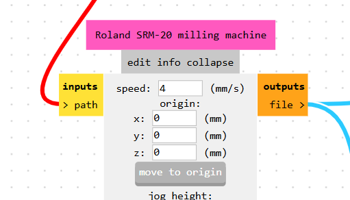
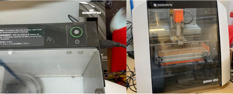
SRM-20 by DGSHAPE
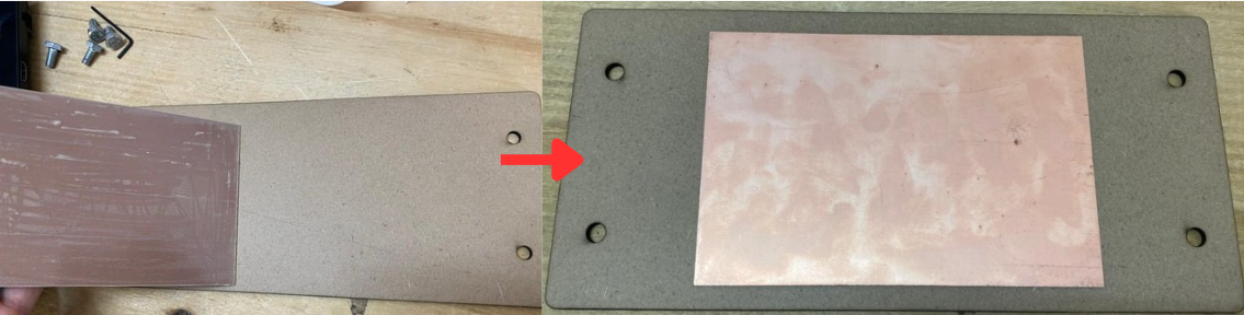
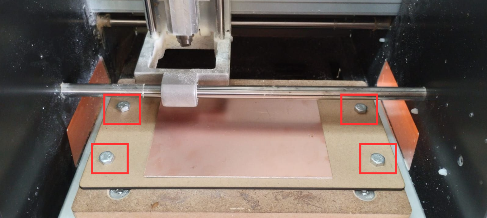
The first step is to secure the PCB substrate onto the sacrificial bed using double-sided tape. The sacrificial bed is fixed to the MonoFab base with the provided screws to prevent movement during machining.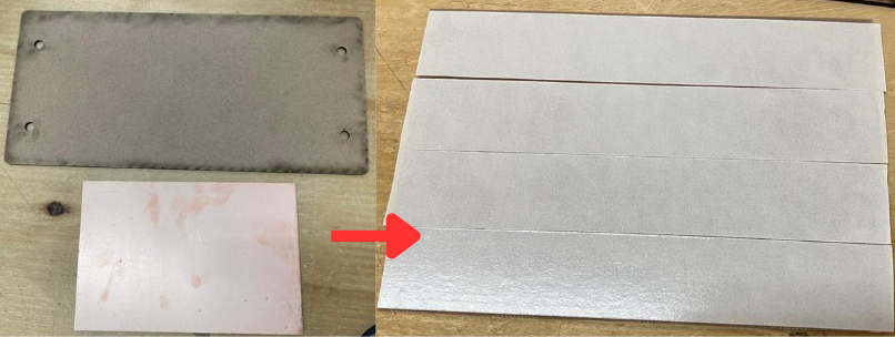
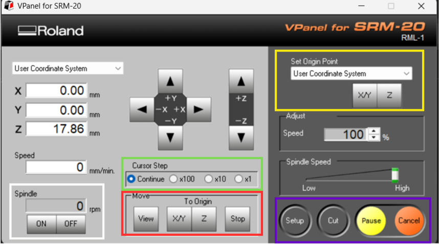
Set Origin Point:
Defines the reference position. The X/Y axes establish the horizontal origin; the Z axis is set separately to define the vertical starting point.
Move:
Allows manual positioning of the toolhead to locate the origin or navigate to a specific point on the board.
Cursor Step:
Adjusts the step size for manual movements, enabling fine or coarse positioning as needed.
Spindle:
Controls spindle rotation. Particularly useful when calibrating the Z axis, allowing the tool to be lowered carefully without damaging it.
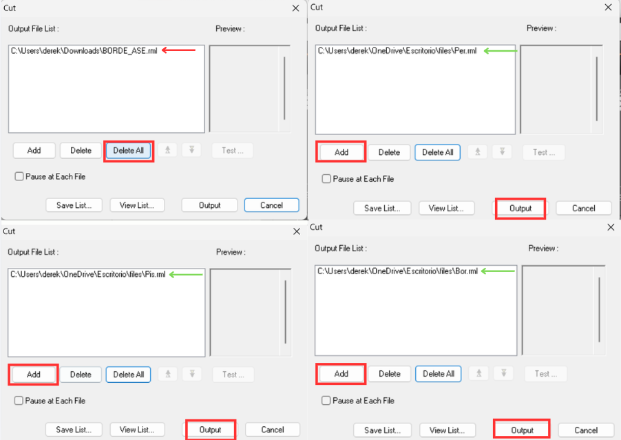
Process Controls
Manages the execution of machining jobs loaded into the queue.
- Click "Delete All" to clear any previously loaded jobs.
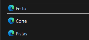
- Click "Add" and select the .rml files generated in MODS.
Drilling → Traces → Outline- Drilling after trace milling risks damaging or lifting copper tracks.
- Cutting the outline first causes the board to move, ruining all subsequent operations.
Tooling and Setup Considerations
The tool dimensions used in MODS correspond to the following physical milling bits:| Process | Tool Diameter |
|---|---|
| Drilling | 0.8 mm |
| Traces | 0.4 mm (flat end mill) |
| Cutout | 2 mm |
Important:
Every time the tool is changed, the Z axis must be recalibrated. Tool length varies between bits, and failing to recalibrate will result in incorrect cutting depth or tool breakage.
- Secure PCB substrate to the bed.
- Set X, Y, and Z origin points.
- Load .rml files in the correct order.
- Run each process sequentially: drilling, traces, cutout.
- Change tools and recalibrate Z between each step.
Soldering Process
With the PCBs milled and cut, the next step is component soldering. Since most components are SMD, pads are pre-tinned before placing components. Pre-tinning consists of applying a small amount of solder to the pad by heating it with the iron and feeding solder from the opposite side until a thin, even layer forms.Once pre-tinned, the component is positioned and soldered by reheating the pad and allowing the solder to reflow and secure it in place.
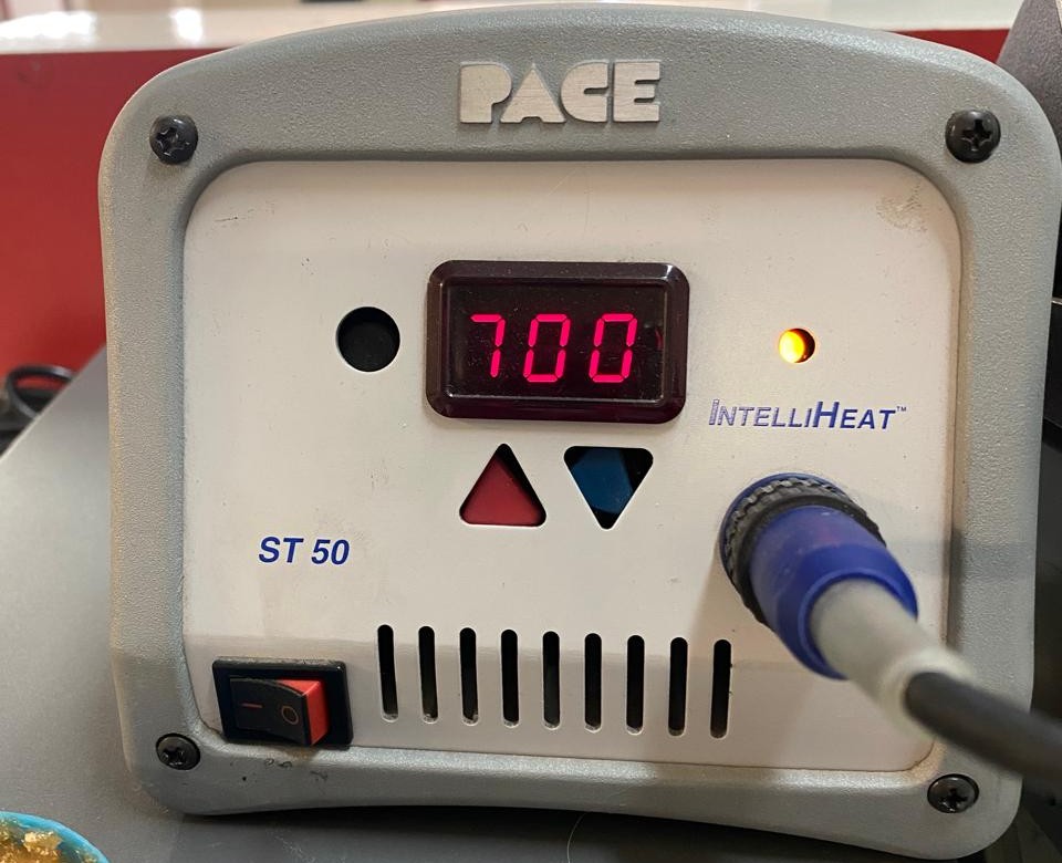
Soldering Temperature Reference
| Temperature (°F) | Application |
|---|---|
| 600–650°F | Delicate components, low thermal mass |
| 650–700°F | General SMD soldering (recommended range) |
| 700–750°F | Through-hole components or larger pads |
| 750°F+ | Heavy ground planes (use with caution) |
Physical Integration
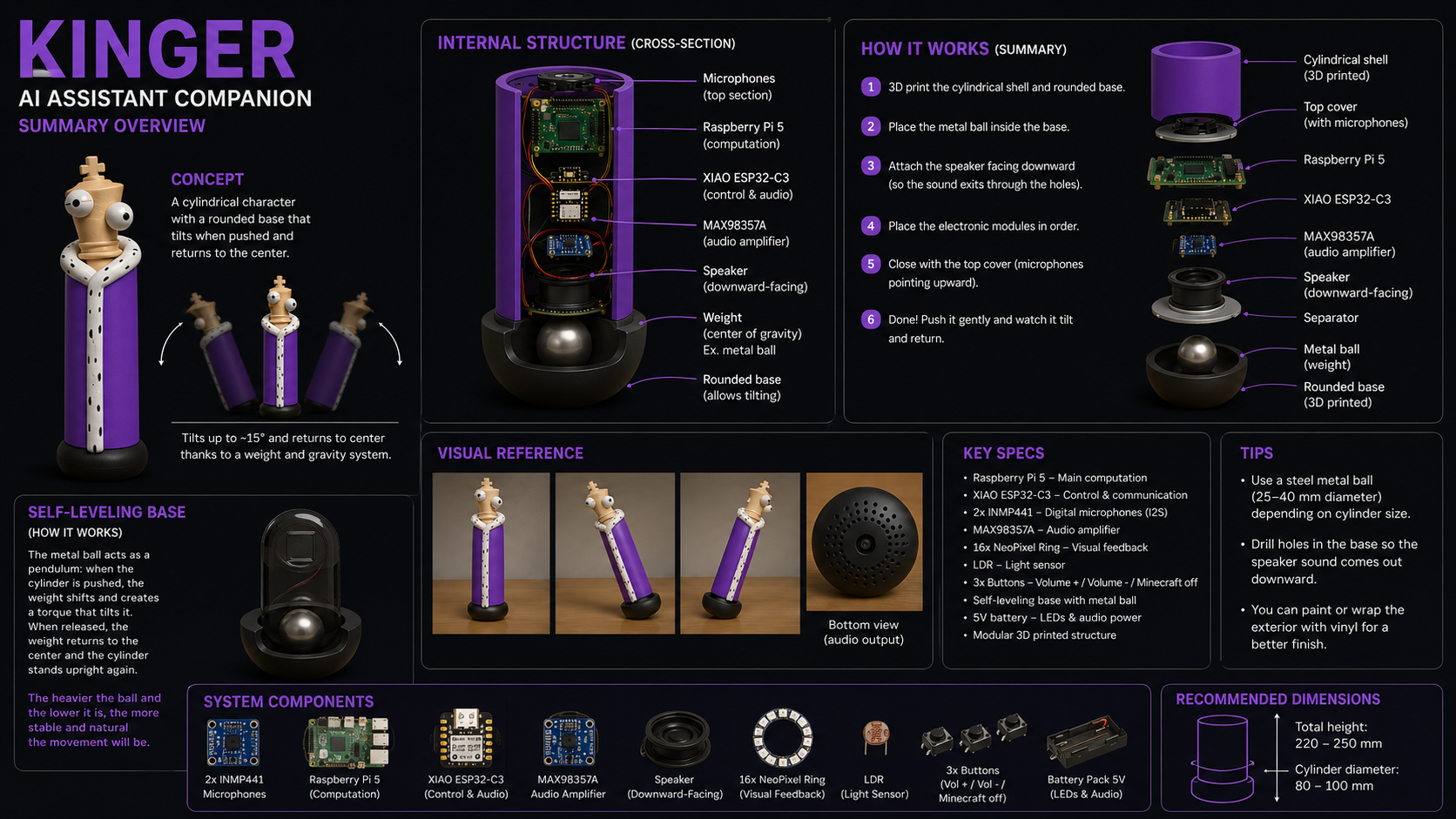
Internal Structure
The internal structure of KINGER is organized as a vertical stack within the cylindrical enclosure. From bottom to top:- Metal sphere: Housed inside the rounded base. Acts as the center of gravity for the self-righting mechanism.
- Speaker (3W 4Ω): Positioned just above the base, facing downward. Audio exits through drilled holes in the base plate, projecting sound outward.
- MAX98357A amplifier: Mounted on the PCB stack directly above the speaker. Receives I2S audio data from the Raspberry Pi and drives the speaker output.
- PCB stack (PCB 1, 2, 3): Stacked vertically using M3 spacers and screws. Contains all signal routing, power distribution, and the XIAO ESP32-C3 module.
- Raspberry Pi 5: Located in the upper section of the cylinder. Provides computational power, manages the audio pipeline, and supplies 5V to the XIAO and NeoPixel ring.
- I2S microphone: Mounted in the top cover, facing upward. Connected to the Raspberry Pi's I2S input bus via the PCB stack.
Enclosure Design
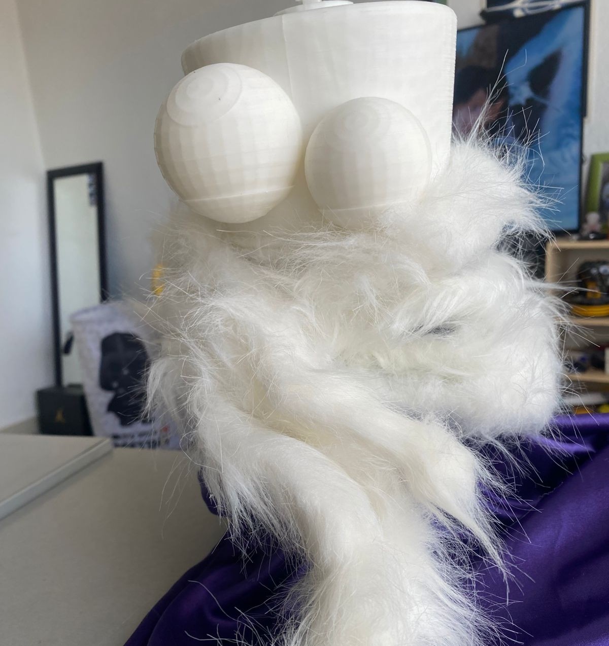
The enclosure consists of two primary components: a cylindrical body and a removable top cover.- Cylindrical body: 3D printed in PLA. Houses all internal electronics. The NeoPixel ring is integrated at a defined height along the cylinder wall or top rim to provide 360° visual feedback visibility.
- Top cover: Removable for maintenance access. Contains the INMP441 microphone positioned with apertures facing upward for unobstructed audio capture.
- Rounded base: Separate 3D printed component forming the self-righting base cavity. Contains the speaker exit holes and the metal sphere chamber.
Packaging and Product Appearance
KINGER is designed to present as a finished consumer product rather than an exposed electronics prototype. The cylindrical form factor, 3D printed shell, and integrated NeoPixel ring create a coherent visual identity that communicates the device's function without exposing internal components.The exterior surface is designed for post-processing: the PLA shell can be sanded, painted, or wrapped in vinyl to achieve a clean, professional finish. The character design derived from a chess piece form gives the device a recognizable and approachable aesthetic suitable for a desktop environment.
Internal organization follows a strict top t bottom hierarchy: microphones at the top, computation in the middle, amplification and speaker at the base. This layout keeps signal paths short, separates audio output from sensitive digital inputs, and concentrates mass at the bottom for mechanical stability.
All ports remain accessible without disassembly:
- USB-C power input is accessible through an opening in the cylindrical body or base.
- GPIO access for development is available by removing the top cover.
- The Raspberry Pi and PCB stack can be fully extracted by lifting the top cover and sliding out the internal assembly.
Integration Challenges
I2S Bus Integration
The KINGER audio subsystem uses I2S for both input (microphone) and output (amplifier), meaning that three separate I2S devices share clock lines on a single bus. The primary challenge is maintaining signal integrity across BCLK and LRCLK when both the microphone pair and the MAX98357A are simultaneously active.Challenge
The INMP441 microphone share the same BCLK and LRCLK lines with the MAX98357A amplifier. Clock skew, capacitive loading, or impedance mismatches on these lines can introduce bit errors or timing failures in the audio stream. Trace length and routing discipline on PCB 1 are critical to preventing these issues.
Internal Space Optimization
The Raspberry Pi 5 occupies a significant portion of the cylinder's cross section. Routing cables from the GPIO header to the PCB stack while keeping the assembly compact requires careful attention to cable length and connector positioning.Challenge
The Raspberry Pi GPIO header sits at one end of the board, while the PCB stack is centered below it. Flat ribbon connectors or short jumper wires must be routed without creating mechanical stress on PCB connectors or obstructing the vertical assembly path.
Port Accessibility
Providing access to the Raspberry Pi USB-C power port and GPIO header without compromising the enclosure's clean exterior finish requires deliberate design decisions:- USB-C access: An opening is cut or printed into the cylindrical body aligned with the Raspberry Pi's USB-C port position. The opening is sized to the USB-C connector footprint to minimize visual impact.
- GPIO access: Available only after removing the top cover. Intended for development and debugging use rather than daily operation.
- Maintenance access: The full internal assembly can be extracted through the top opening of the cylinder after the top cover is removed. No tools are required for normal maintenance operations.
Expected Result
The integrated KINGER system is designed to function as a standalone desktop assistant capable of:- Capturing voice input through digital I2S microphones.
- Processing audio locally on the Raspberry Pi 5.
- Delivering audio responses through the amplified speaker system.
- Providing visual feedback through the NeoPixel ring.
- Accepting user input through physical buttons and the light sensor.
- Operating without external computing infrastructure — all processing occurs on-device.
- Presenting as a finished, self-contained product with a clean exterior and accessible internal architecture.
Integration Summary
KINGER integrates custom PCB electronics, a dual-processor embedded computing system, a fully digital audio pipeline, WS2812B LED feedback, physical user controls, environmental sensing, and a self-righting 3D printed mechanical enclosure into a single cylindrical desktop device. The system architecture, schematic, PCB layouts, and manufacturing workflow were all completed and verified prior to final assembly.
Results
BOARDS