The objective for this week was to use a professional EDA tool to design a PCB, adding at least one LED and a button to a microcontroller circuit. I focused on learning KiCad to create both the schematic and the physical board layout.
Group Assignment
Using test equipment to observe the operation of a microcontroller circuit board.
EDA WorkflowKiCad 8.0
For this assignment, I designed a custom board based on the Seeed Studio XIAO RP2040. The workflow consists of creating the schematic, associating footprints, and routing the tracks on the PCB.
Schematic Design
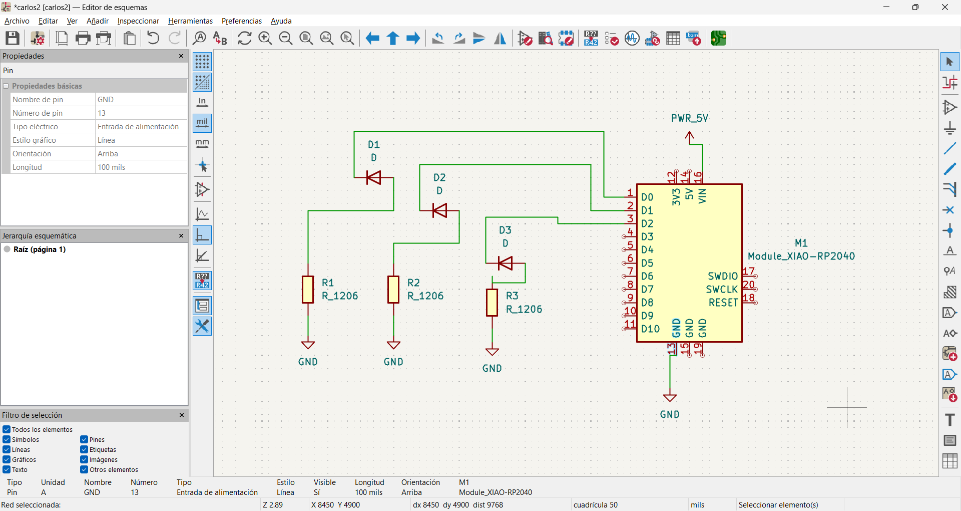
In this design, I used the KiCad schema editor to configure a board based on the XIAO RP2040 microcontroller. My main goal was to establish a stage of control of outputs with current protection and regulation.
PCB Layout and Routing
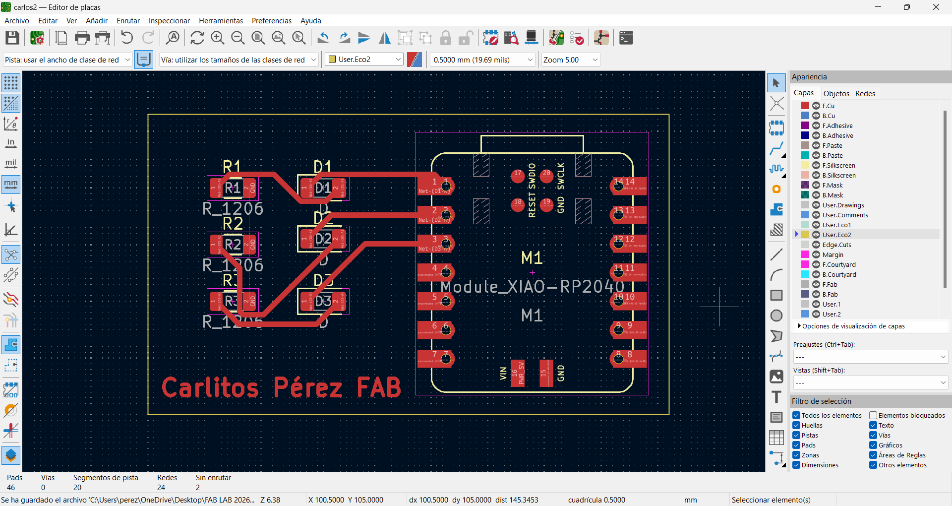
In the KiCad PCB editor, I went from schematic to physical design by placing the XIAO RP2040 module and 1206 components. I plotted the tracks on the top layer to connect the digital pins with the diodes and resistors, ensuring the return to GND at a common node. Finally, I defined the plate cuts and customized the design with my signature on the screen printing to leave it ready for manufacturing.
3D Visualization and Design Validation
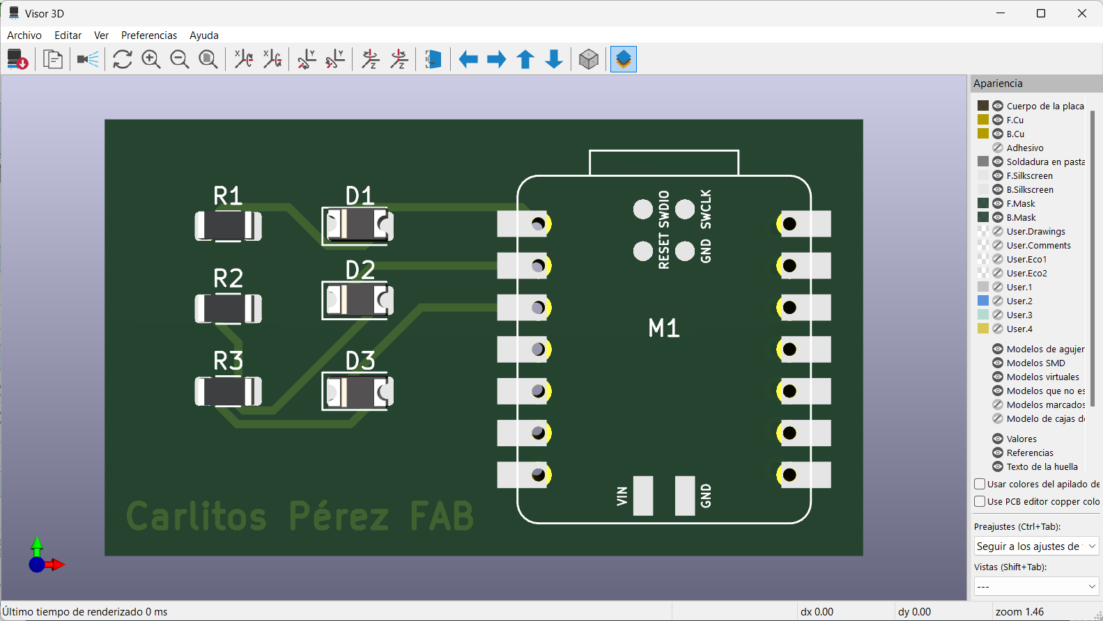
I generated a preview in the KiCad 3D Viewer to validate the final appearance of the board before commissioning it. In this rendering, I confirmed that the XIAO RP2040 module and 1206 components are well distributed, with the copper tracks integrated under the green welding mask. In addition, I checked that the custom signature and pins labels are legible, ensuring that the design is physically viable and aesthetically clean.
Gerber2PNG
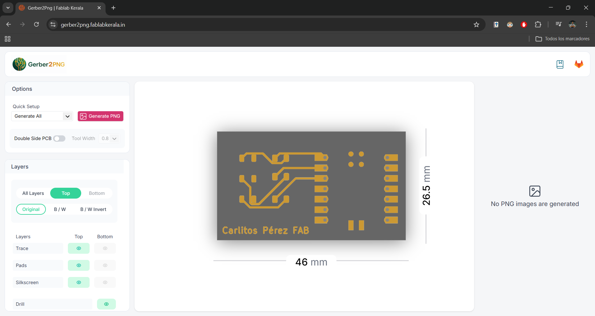
At this stage, I used the Gerber2PNG tool to convert my PCB manufacturing files into high-resolution images. I uploaded the Gerber files and got a clear preview of the tracks, pads and screenprint with precise dimensions of 46 x 26.5 mm, which is essential for validating the actual size before production.
Gerber to PNG Conversion and Scale Verification
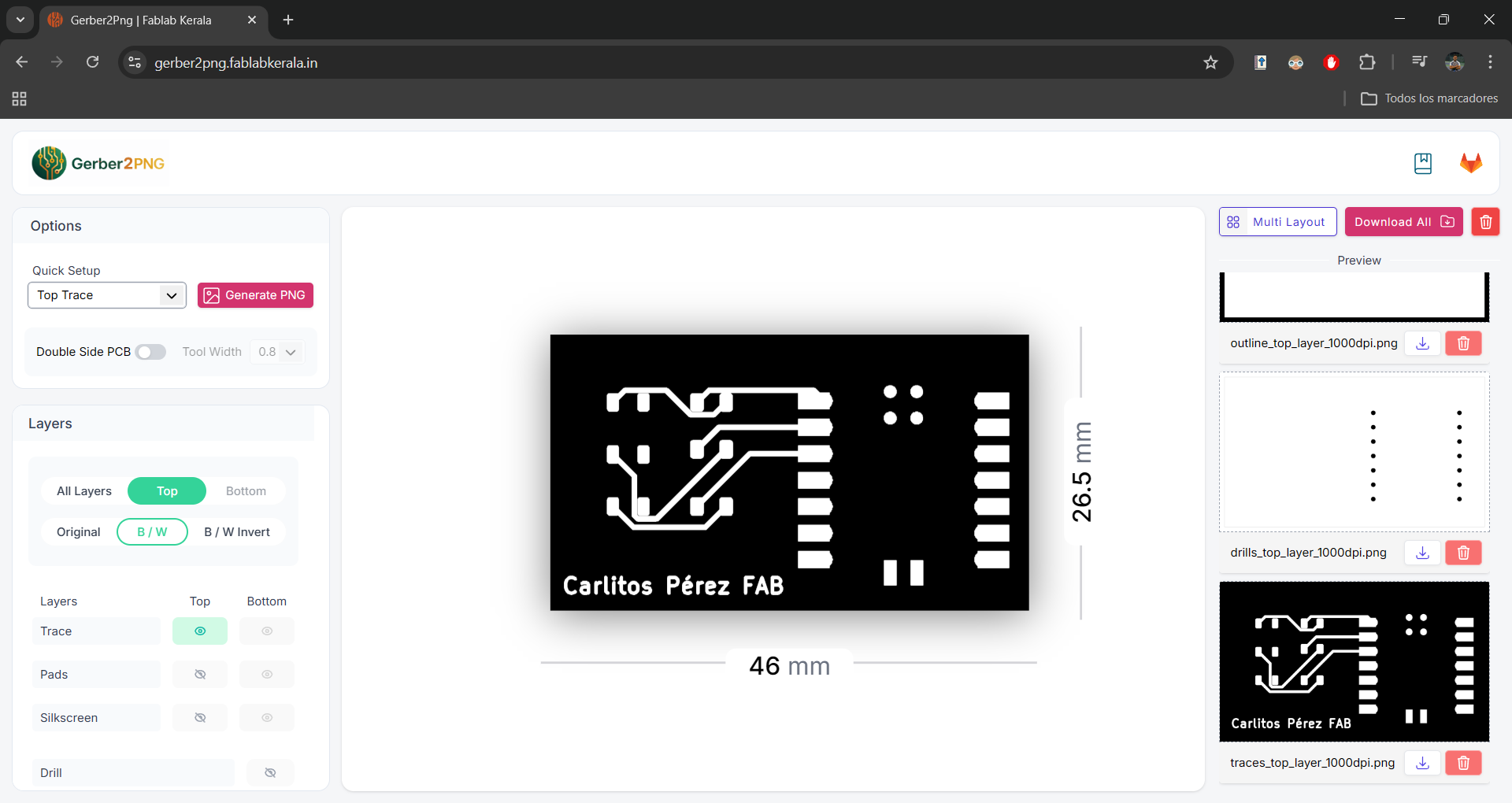
This page is extremely useful for local digital manufacturing processes, as it allows: Generate bitmaps: Create PNG files that can be used directly in CNC machine control software or laser cutters. Insulating layers: Allows you to separate the tracks (traces) from the holes (drills) to mill the plate by steps. Verify scales: Ensures that components fit perfectly into the physical world before expending material.
Workflow Selection and Machine Setup in mods
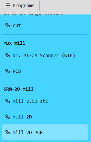
On the mods platform, in the programs section, I selected the workflow for my machine: the Roland SR-20, configuring it specifically for circuit milling (2D PCB mill).
Toolpath Configuration
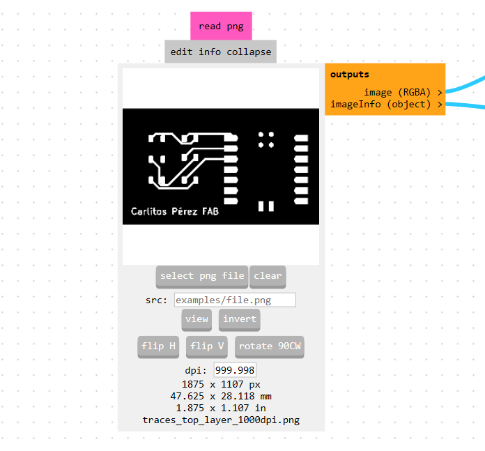
I uploaded the PNG file of the tracks (traces) into the software, validating that the physical dimensions matched the original design. For the engraving process, I selected the 60° V-bit tool (#501), setting the specific parameters for a defined and precise path
Offset Strategy and Toolpath Calculation
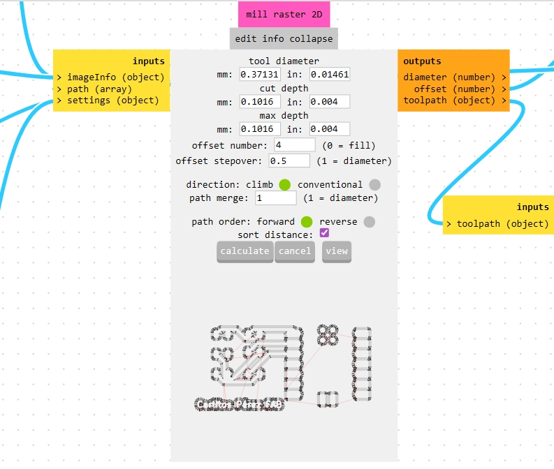
I set the diameter of the tool to 0.4 mm and defined a 4-pass offset to ensure optimal insulation between tracks. After clicking 'Calculate', the software automatically generated a 3D visualization that allowed me to inspect the cutting paths and validate the final finish before sending the file to the milling machine.
Exporting for Fabrication
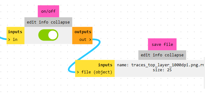
I manually adjusted the point of origin (X, Y, Z) to 0, as it is essential for the milling machine to recognize our initial position. Unlike the default setting of 10, 10, 10 which is sometimes used in the Fab Lab, I needed to reset the coordinates for this project to ensure that the engraving starts exactly where the material ends. Enabled the input option in the workflow so that the output file is automatically downloaded at the end of the calculation. Once I obtained the file, I proceeded to upload it into the VPanel software to manage the control of the milling machine and execute the manufacturing process.
The Roland SRM-20 MonoFab
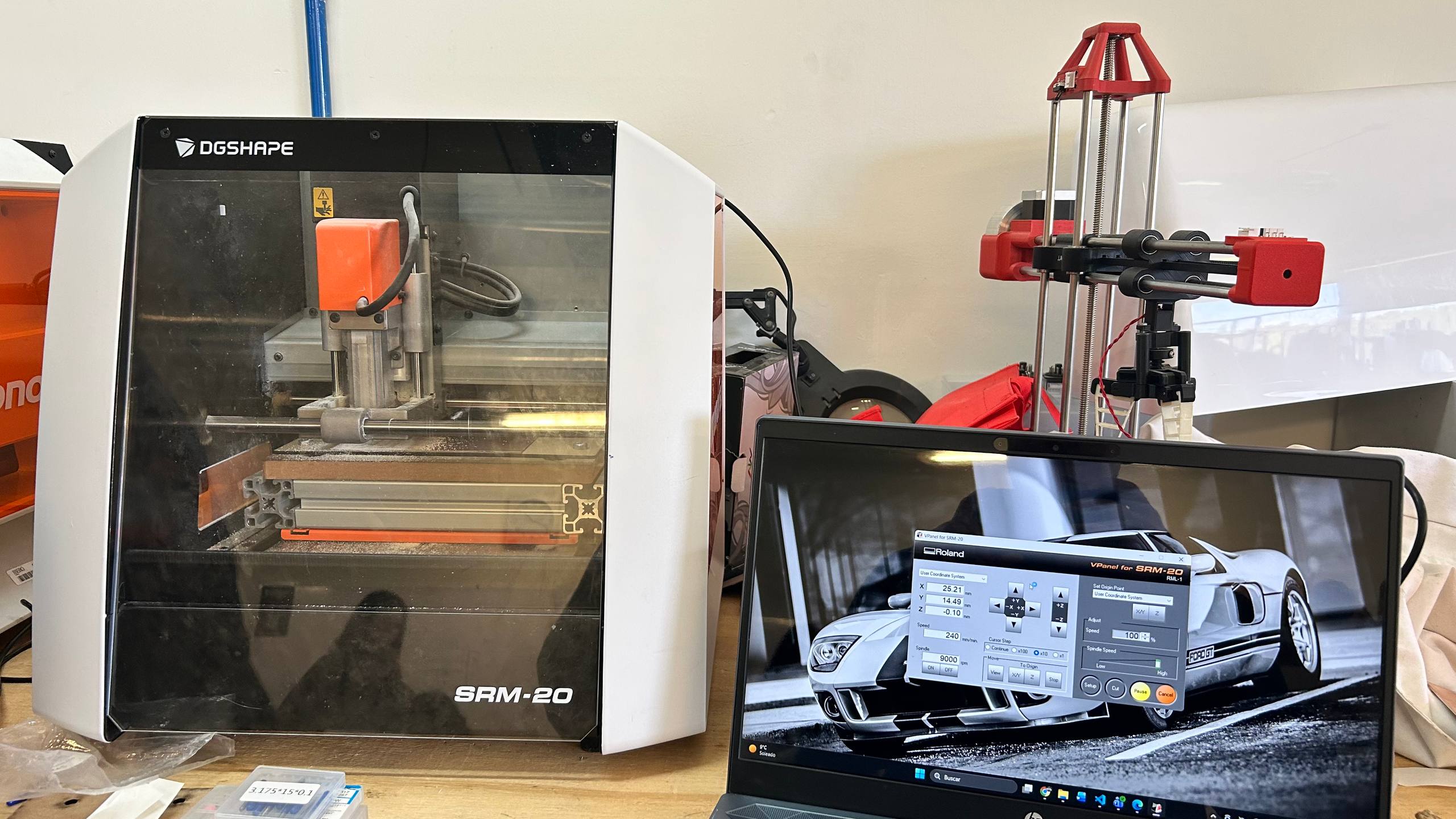
For the board manufacturing, I used the Roland SRM-20 MonoFab, a high-precision desktop milling machine designed for rapid prototyping of PCBs. This machine allows for millimetre engraving of the tracks and precise contour cutting, ensuring a professional finish on surface assembly components (SMD).
Workholding and Material Preparation
I prepared the copper plate by applying double-sided tape to its base, ensuring a uniform hold to prevent vibrations. Subsequently, I fixed it firmly on the machine’s slaughter bed, ensuring that the surface was perfectly level for a homogeneous milling.
VPanel Setup and Axis Calibration
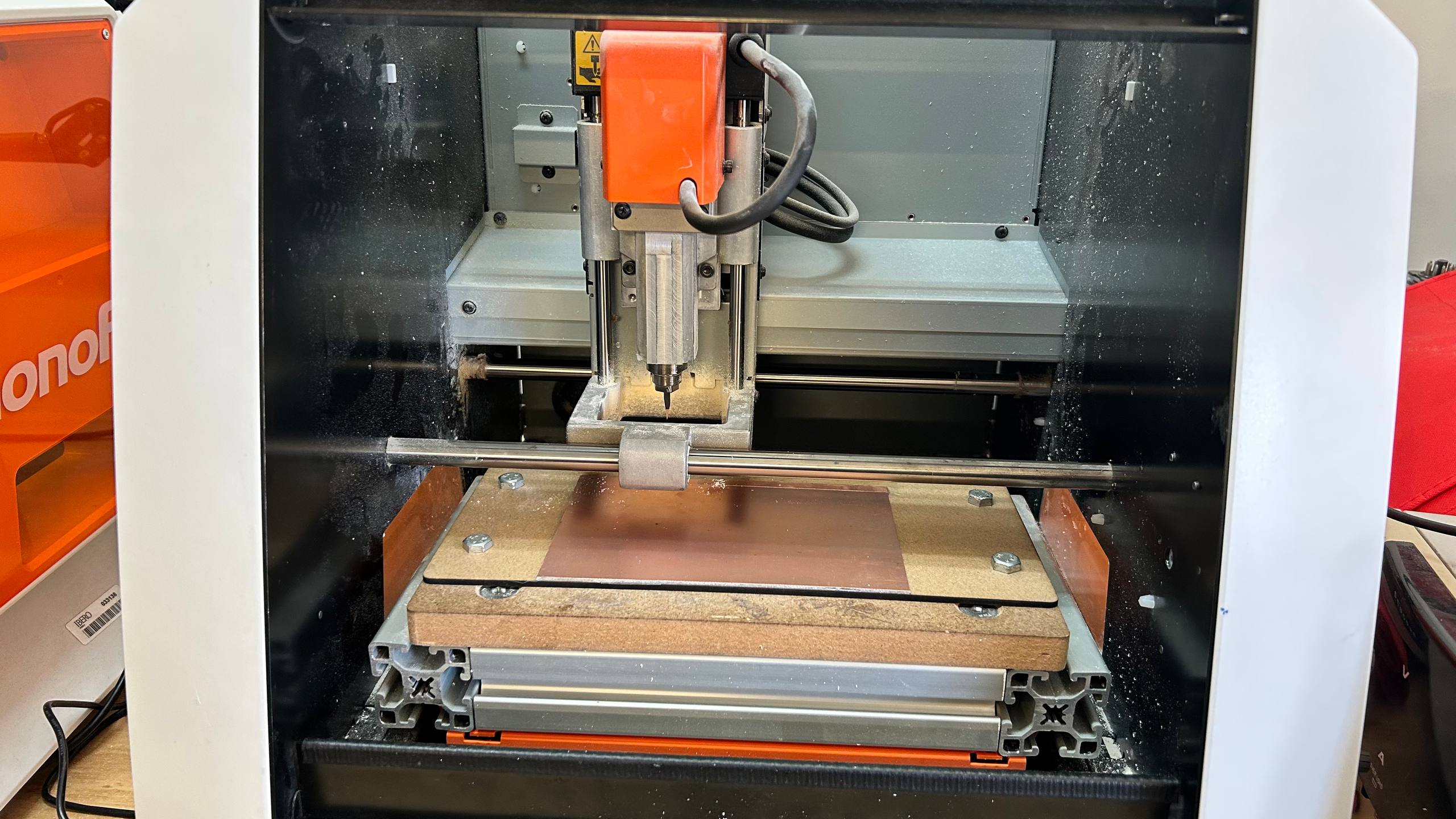
I fixed the slaughter base to the SRM-20 platform and, using the VPanel interface, set the origin point manually. After validating the position of the axes, I imported the cutting file and executed the 'Output' command to start milling the tracks.
Contour Cutting and Final Board Separation
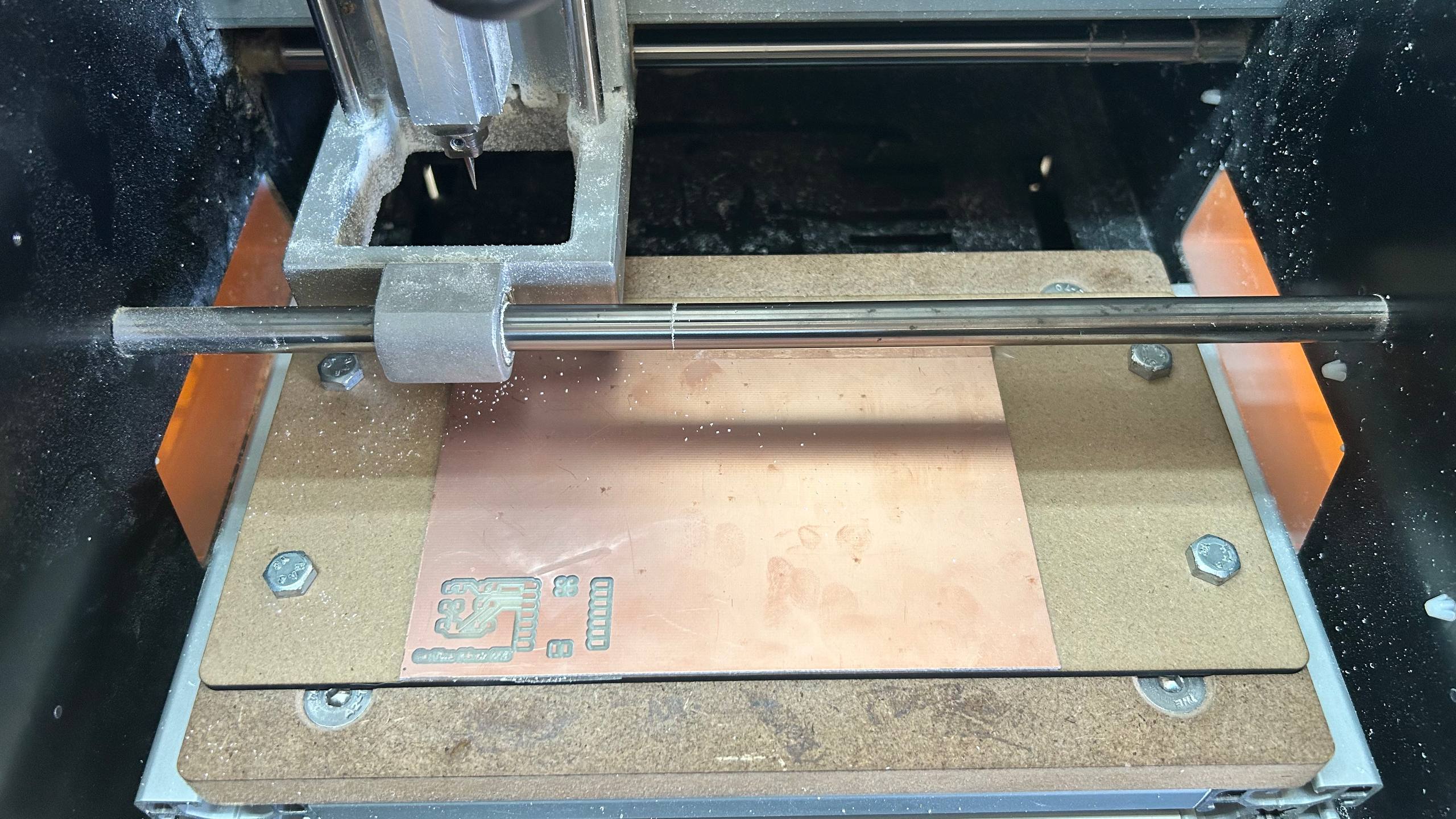
After finishing the engraving of the tracks, I uploaded the outcut file into the control software. After validating that the cutting tool was correctly positioned, I executed the final command to physically separate the plate from the base material.
Electronic Assembly
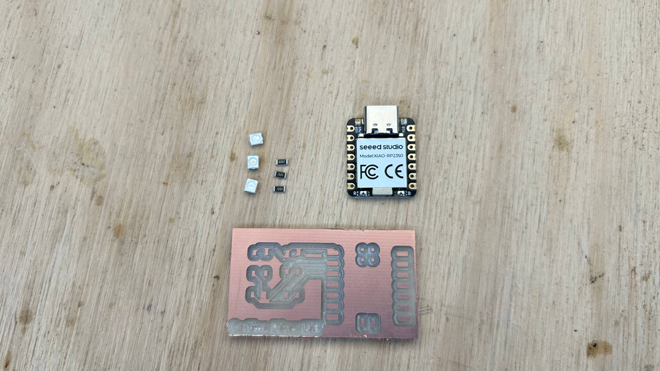
Once the components are ready, I proceeded with the soldering process onto the PCB.
Soldering
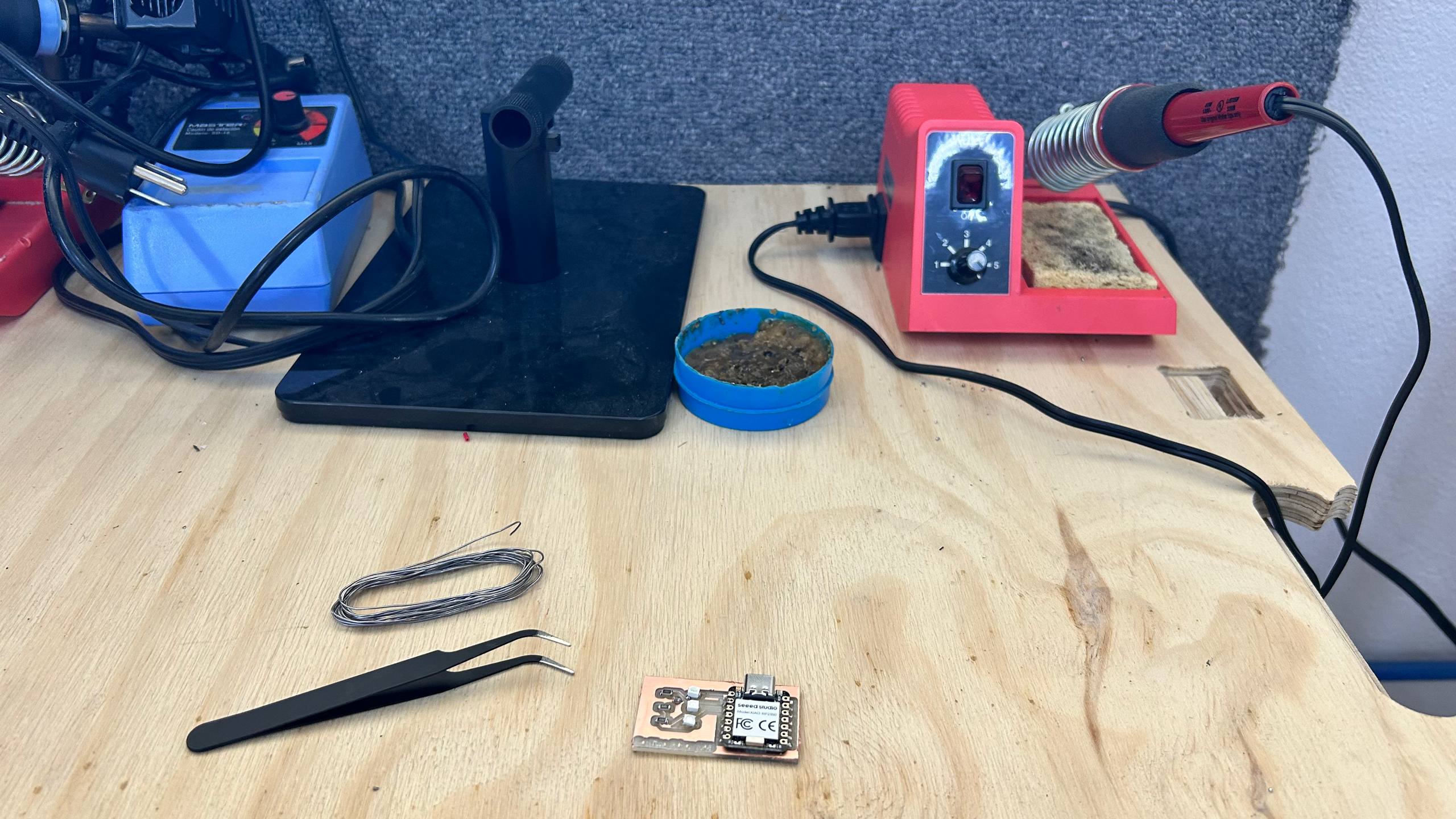
To ensure optimal welding technique, I supplemented my training with an additional technical session on surface assembly components (SMDs). I used a fine-tipped welding station with high quality tin and precision pliers to handle and secure each component in its exact position on the plate pads.
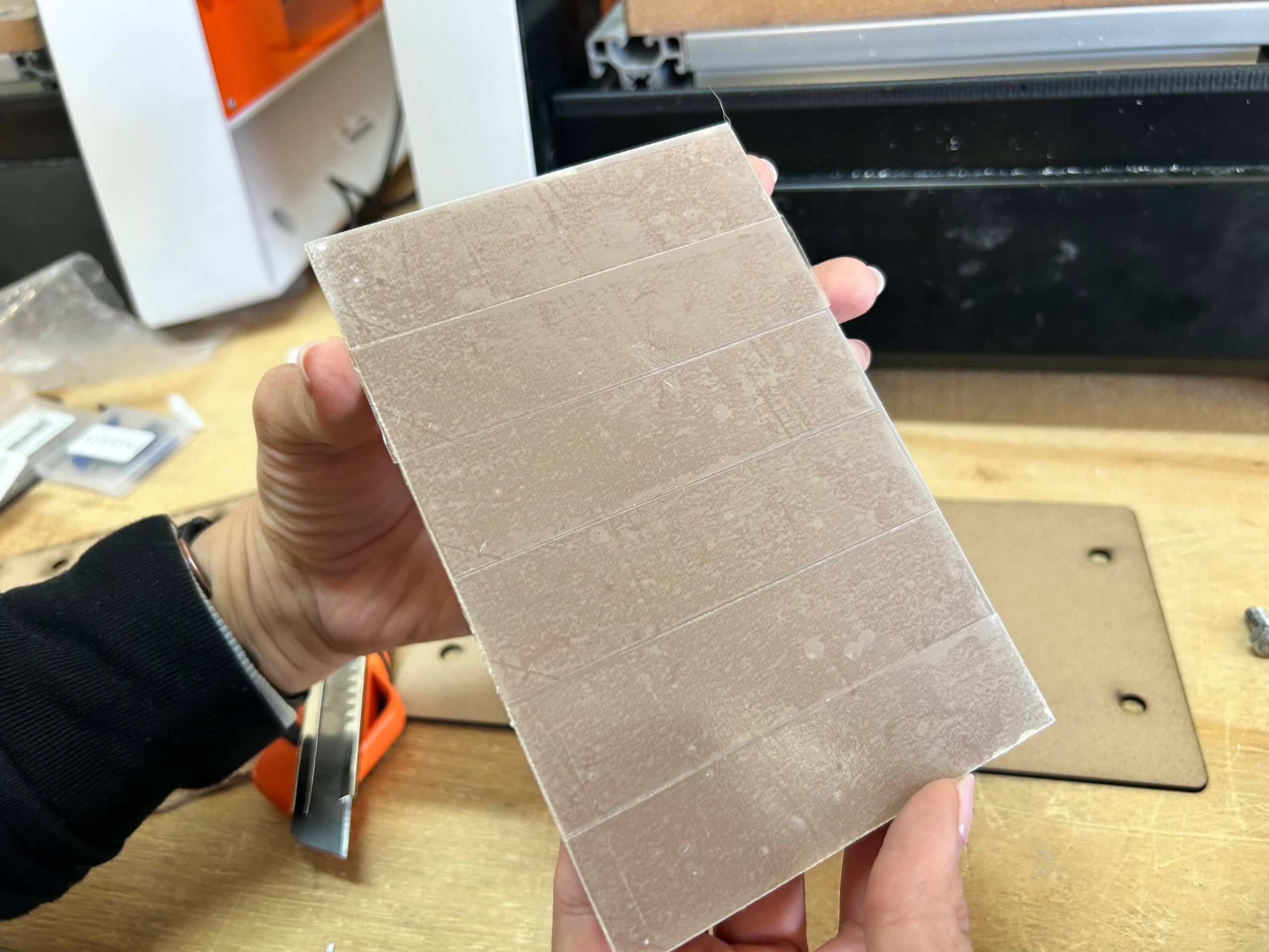
Post-Milling Inspection and Error Analysis
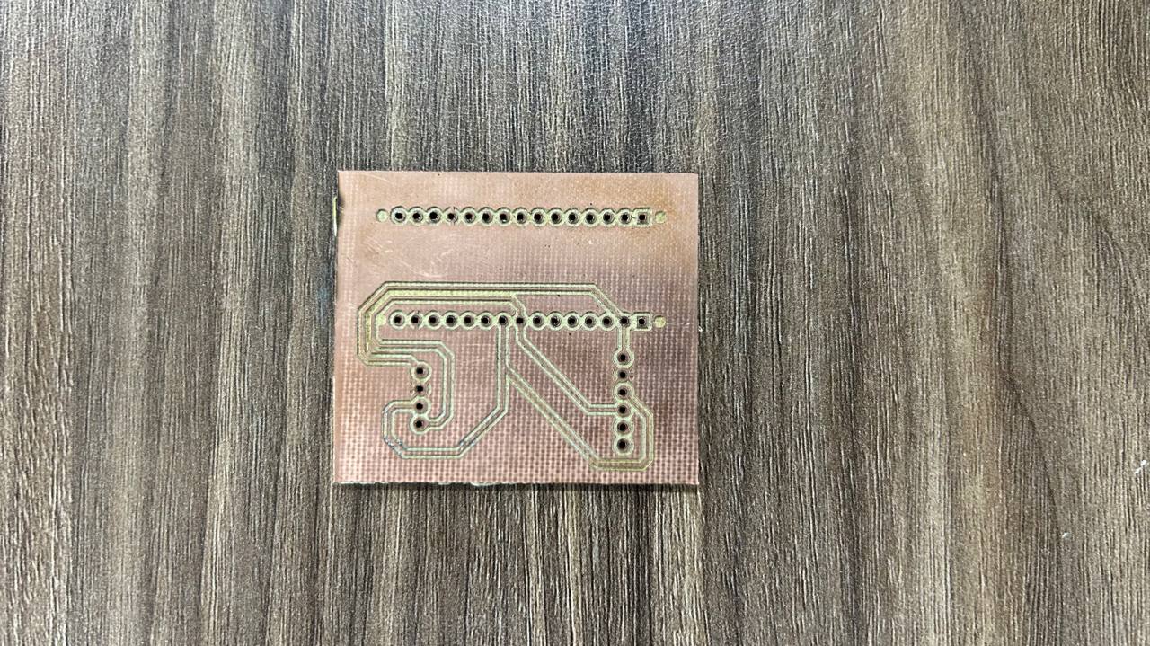
In the final observations, I identified critical errors in the design of the tracks: the thickness was insufficient and short-circuits were presented due to line overlapping. Due to these continuity failures, the system does not respond when connected and the LEDs do not light up. I decided to iterate the design, adjusting track widths and isolation distances to ensure functionality in the next version.
Post-Milling Inspection and Error Analysis
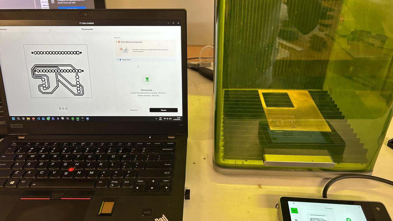
The image shows the engraving process in progress using the xTool F1 Ultra, where I prepared and loaded the design of a technical circuit into the software, while the machine performs the engraving on a gold metal plate safely under its green protective cover, all of this monitored simultaneously through the external touch control screen located on the side.
Post-Milling Inspection and Error Analysis
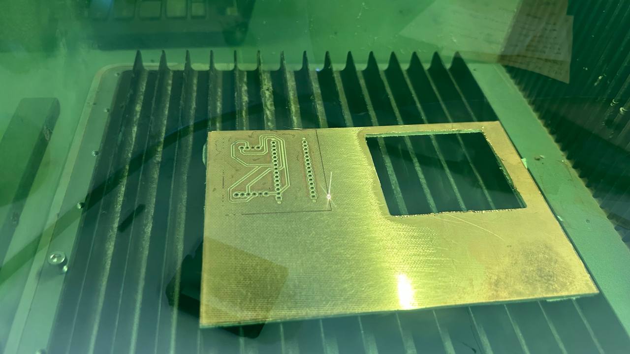
In the image, I show the xTool F1 Ultra at full execution, accurately recording the intricate design of a circuit on a copper plate resting on the striated base. I captured the exact moment when a point of intense light, the laser beam, moves through the material, leaving in its path the pattern of detailed tracks and holes for the prototype. The entire scene is observed through the characteristic green safety filter of the deck, ensuring safe operation while monitoring detailed progress that is faithfully transferred from digital design to the physical piece.
Post-Milling Inspection and Error Analysis
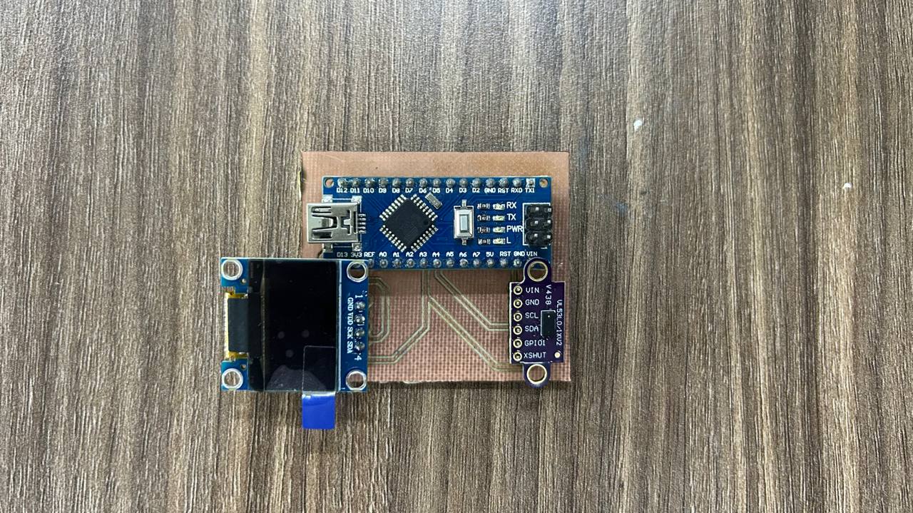
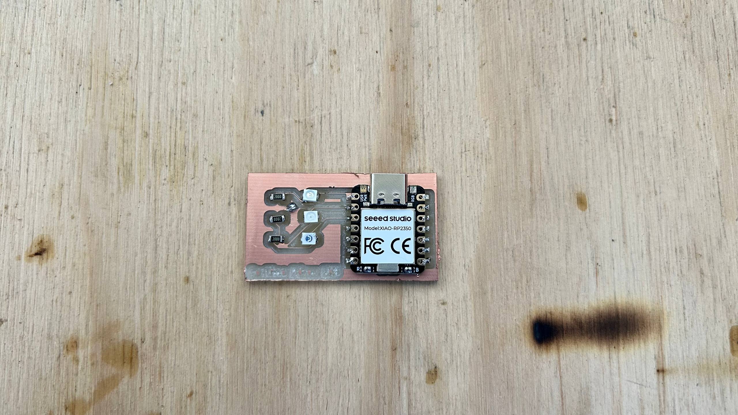
Finally, we have completed the assembly of the printed circuit board (PCB). The result, as seen in the image, is very satisfactory and functional. After the manufacturing process with xTool and manual welding, we have managed to integrate all key modules. The copper-based PCB has clean and well-defined traces, on which we have successfully assembled the following components: