This week focused on the design of a printed circuit board (PCB). We learned to use KiCad to create schematics, assign footprints, and route tracks to build a functional electronic system using the Arduino Nano micro-controller.
Group Assignment
Characterizing the laboratory equipment and testing design rules for PCB production.
KiCad Workflow EDA Software
For the electronic design, I used KiCad 9.0. This software allows a professional transition from a conceptual diagram (Schematic) to a physical layout (PCB) through a structured workflow.
Project Initialization and File Generation
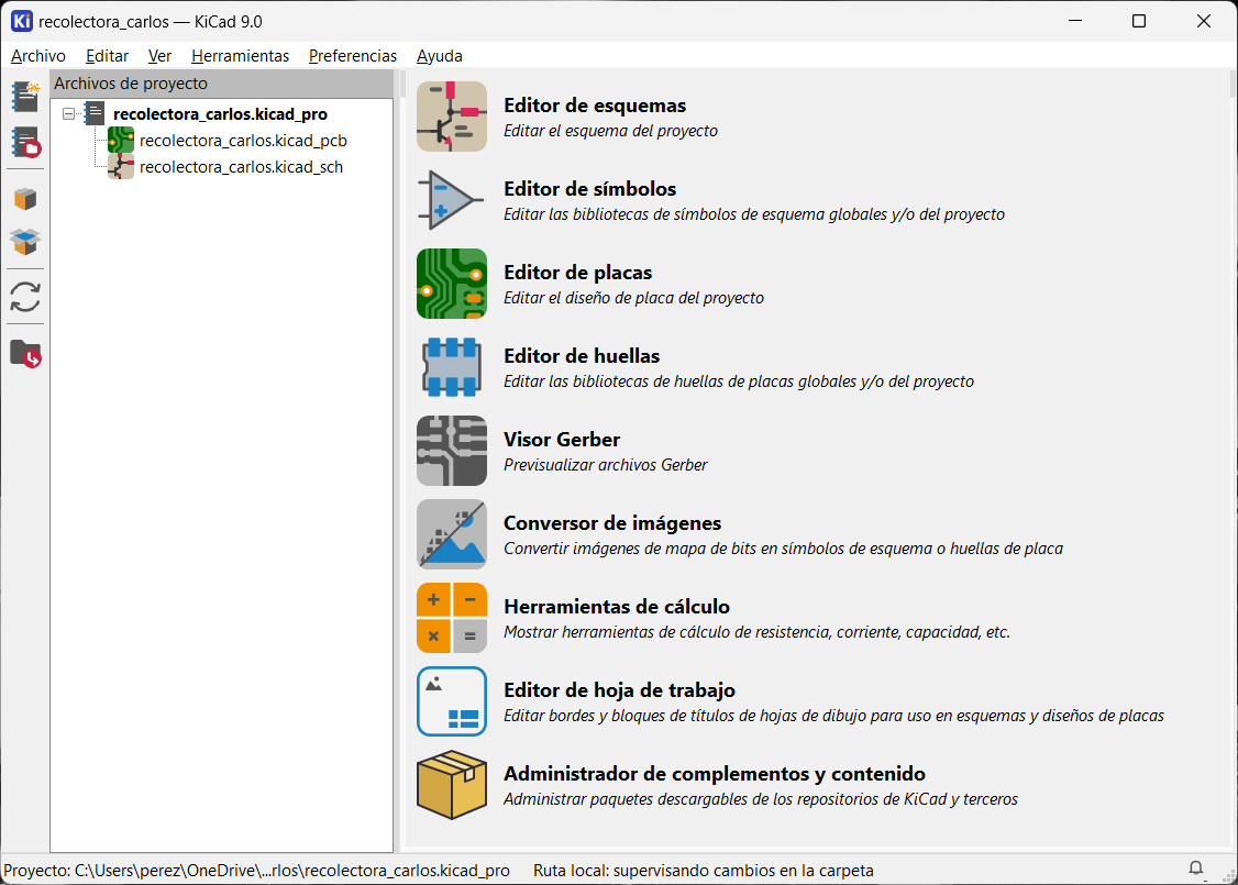
When you open KiCad and create a new project, we select the target folder and the program automatically generates two main files: one for the schema editor and another for the board editor (PCB).
Component Insertion and Selection
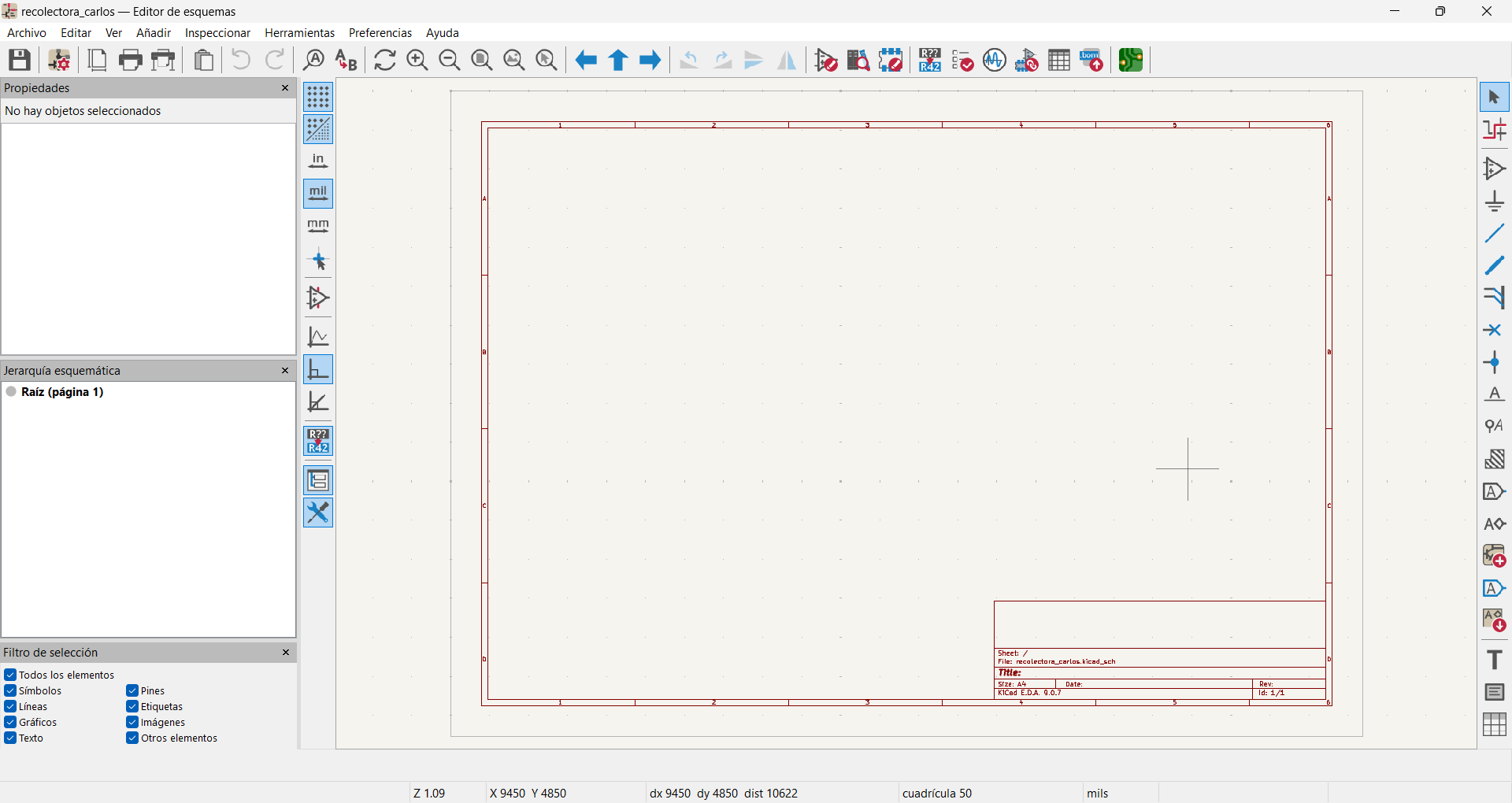
Once in the schema editor, we can press the 'A' key or click on the 'Add Symbol' icon (Place Symbol) to start placing components.
Critical Component Selection and Linkage
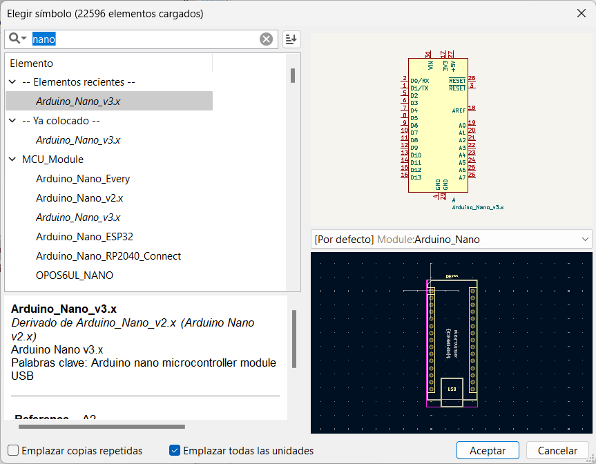
Activating this command will open the symbol library where we can search for necessary components. It is essential to check that the specifications and dimensions match our requirements; otherwise, the project may fail or not work. When the symbol is selected, its footprint will be automatically linked if it is predefined.
Instantiation of components and adaptation of peripherals
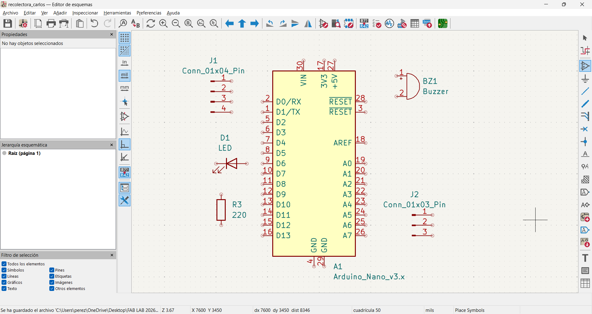
We proceed to insert the components into the scheme. For this design, I used a buzzer, an LED and a resistor. Since the servo motor and ultrasonic sensor are not directly in the standard library, I used 3- and 4-pin connectors respectively to represent their connections. Finally, I integrated the Arduino Nano module as a control unit.
Wiring of the Electrical Scheme and Interconnection
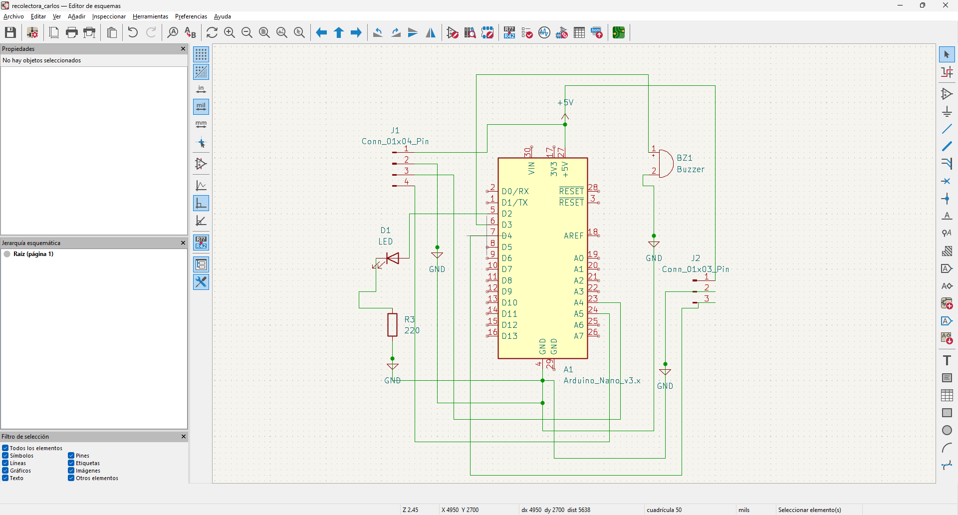
Once the components are inserted, we proceed to make the electrical connections (wires). With the properly interconnected scheme, the design is ready to be transferred to the board editor (PCB Editor).
Import Components and Networks (Netlist)
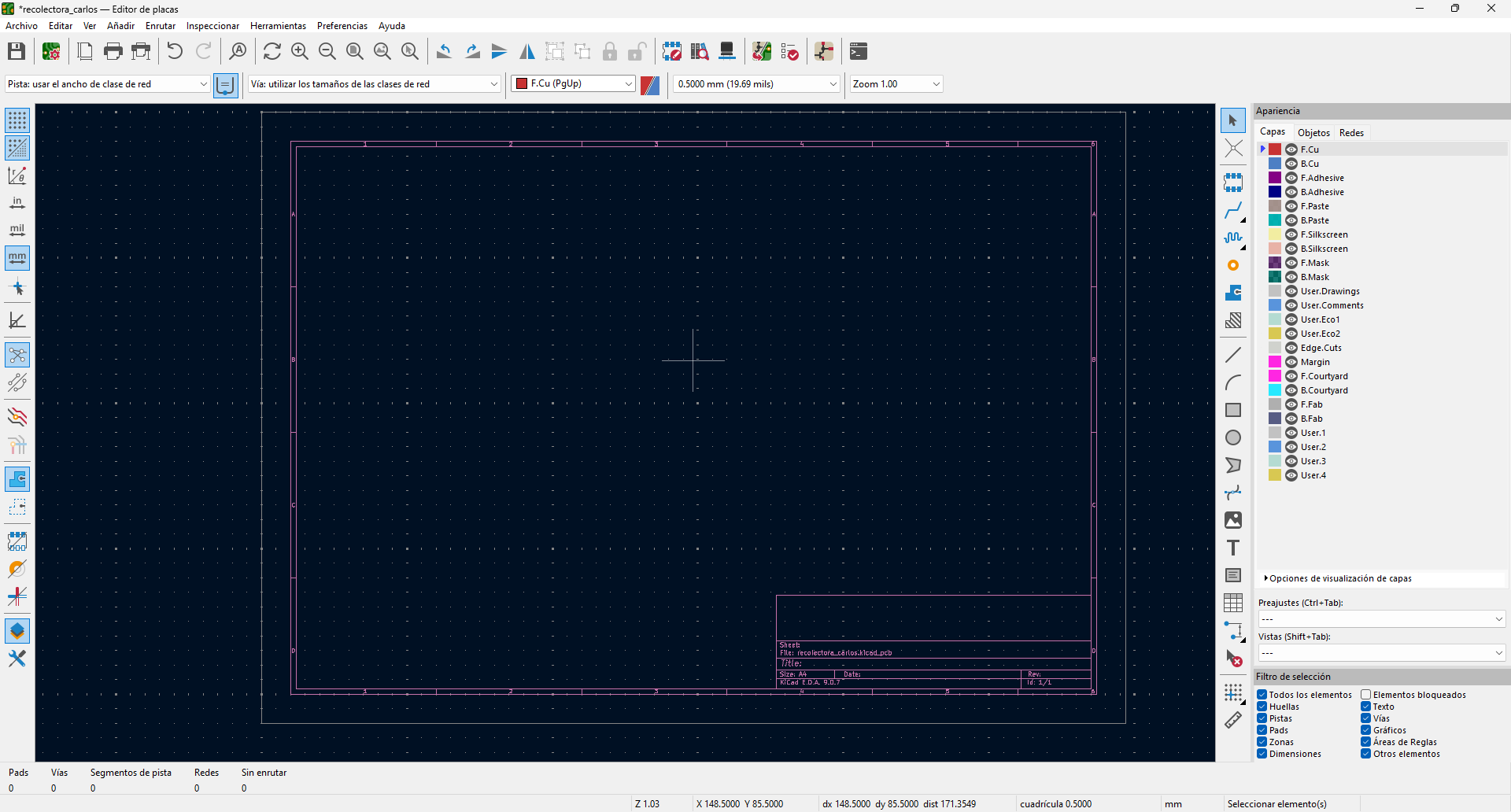
When opening the PCB Editor, we can synchronize the design directly by pressing the F8 key or clicking on the icon in the top bar (a schematic sheet with a green arrow towards a board). Both options run the 'Update Board with Schema Changes' function, which automatically transfers all components and connections to the physical design environment.
Footprints Update Parameters
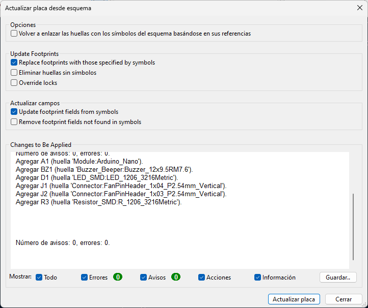
In the update window, we must keep 'Replace footprints with those specified by symbols' and 'Update footprint fields from symbols' checked. This ensures that any changes made to the scheme are accurately reflected in the design of the plate
Perimeter Definition and Plate Geometry
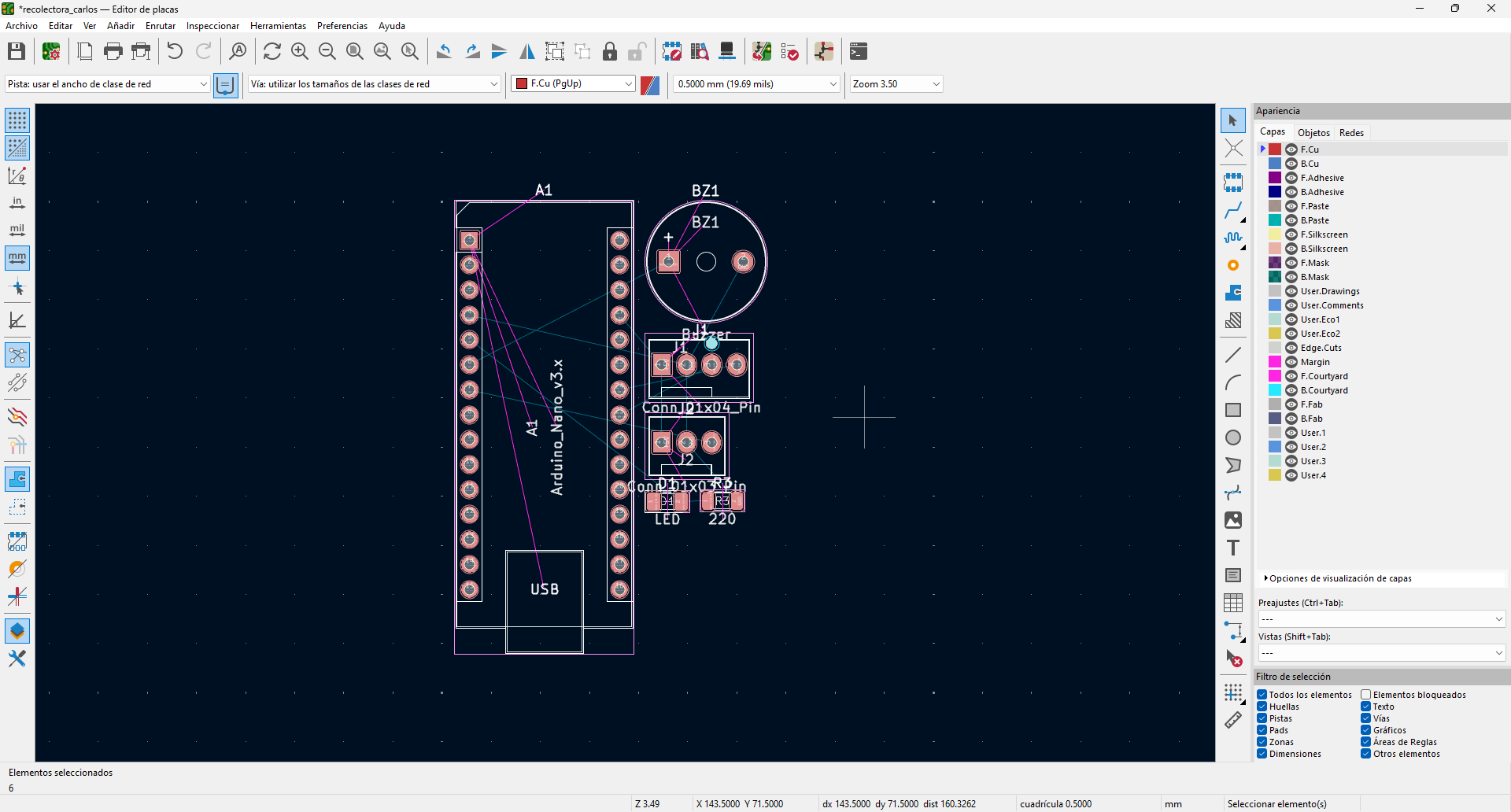
In the sidebar layer manager, we select the Edge.Cuts layer to activate it. Once selected, we proceed to draw the outline or perimeter that will define the physical form of our printed circuit board (PCB).
Track routing and copper layer management
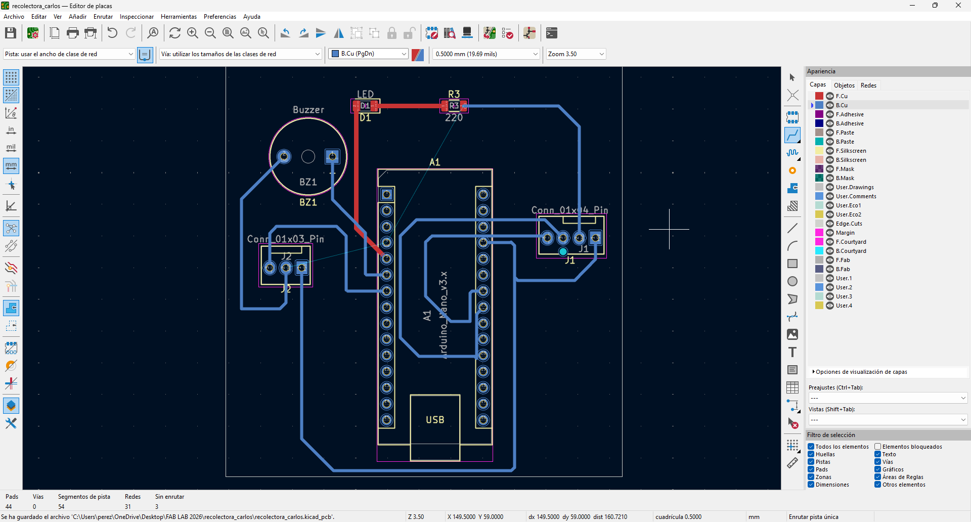
When plotting the clues, we must ensure that they dont cross each other to avoid short circuits. KiCad facilitates this task by using ratsnest (elastic lines), which tells us the destination of each pin when selecting it. In addition, we must distinguish between the copper layers: the red tracks belong to the top layer (F.Cu), while the blue ones correspond to the bottom layer (B.Cu).
Closing of Layers and Electromagnetic Shielding
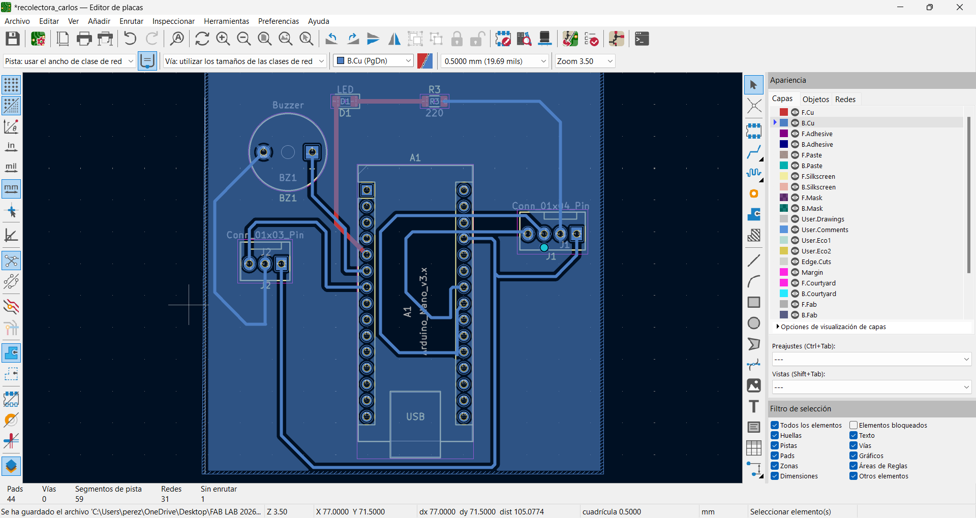
Finally, I performed the route of tracks in two layers, defined the physical outline in Edge.Cuts and added a plane of mass to leave the plate ready for manufacturing.
PCB Anatomy: Layer Management and Functionality
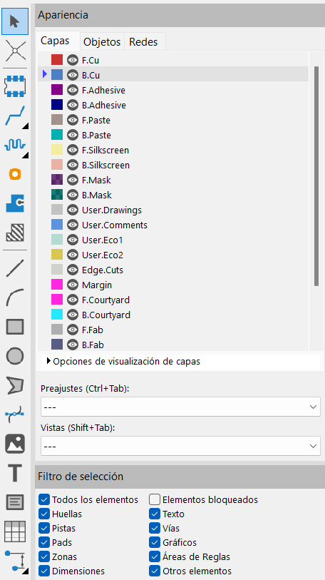
In PCB design, layers function as "transparent sheets" stacked one on top of the other. Copper layers (electrical conduction) F.Cu (Front Copper - Red): This is the top layer of copper. It is used to place tracks and pads on the top side of the plate. B.Cu (Back Copper - Blue): It is the lower layer of copper. As seen in your picture, this is where you have most of your connections and the plane of mass (the striped blue background). Layers of Mask and Paste (Manufacturing) F.Mask / B.Mask (Solder Mask): These are the layers of "welding mask". It is the varnish (usually green) that covers copper so that it does not rust and to prevent tin from sticking where it should not. The voids in this layer allow the components to be welded. F.Paste / B.Paste: Used only if you are soldering surface mount (SMD) components with an oven. They serve to manufacture a template (stencil) that applies the welding paste. Silk-screen layers (visual information) F.Silkscreen / B.Silkscreen: It is the white "ink" that is printed on the plate. Here are the names of components (such as BZ1, A1, R3), logos and labels that help you know where to weld each thing. Help and Design Layers Edge.Cuts (Yellow/Pink): It is perhaps the most important after copper. It defines the physical edge of the plate. Its the line that tells the machine where to cut the bakelite. F.Courtyard / B.Courtyard: Defines the physical space that occupies the component. It lets KiCad tell you if youre putting one component on top of another or too close. F.Fab / B.Fab: Manufacturing layers. They contain simplified drawings of the components to create technical documentation or assembly manuals. User.Drawings / User.Comments: These are free layers. You can use them to write personal notes, dimensions or guides that will not be printed on the final plate.
Dynamic Validation and Transient Simulation (SPICE)
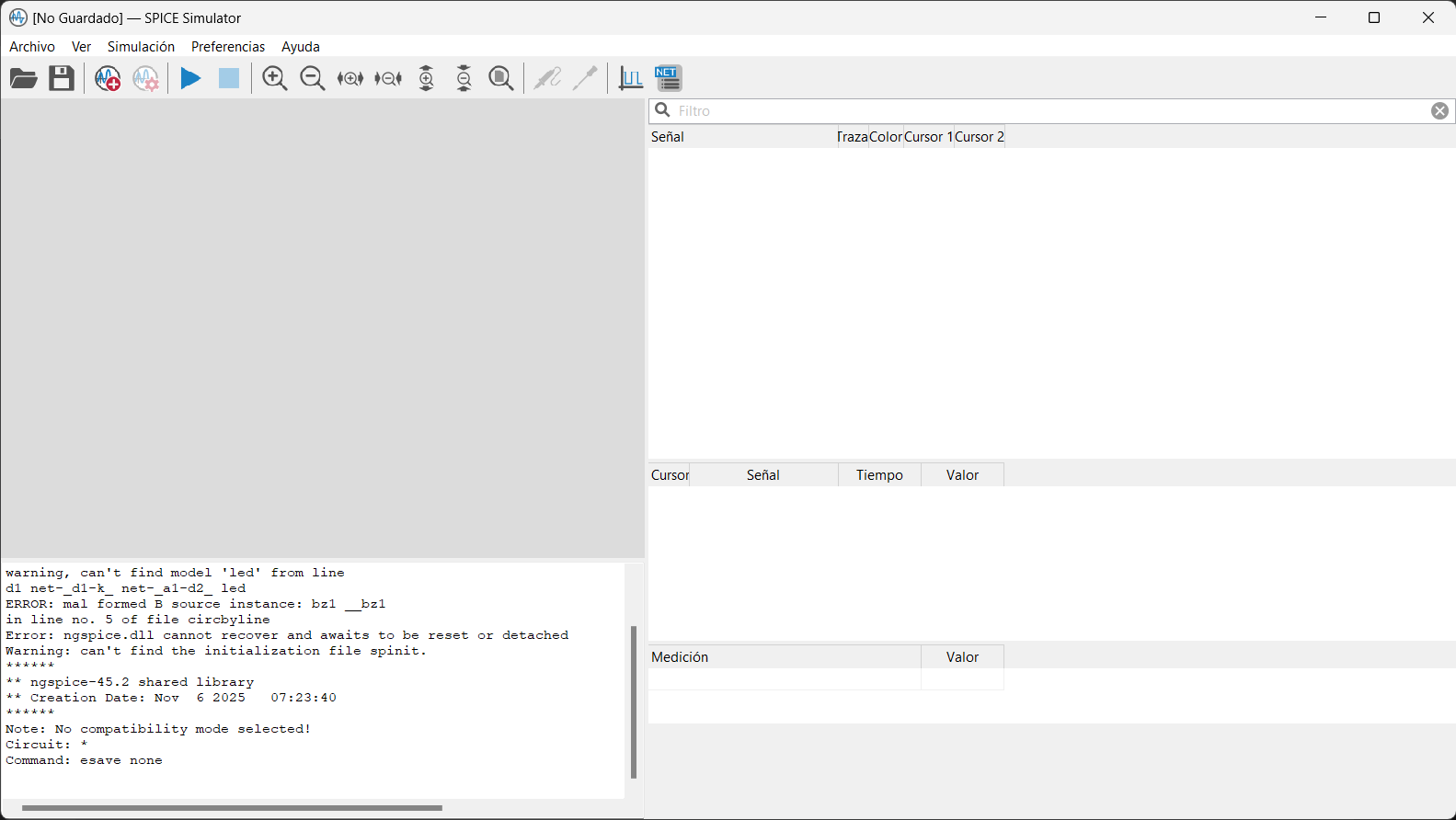
To check how it works, I opened the Simulator from the 'Inspect' menu in the schema editor. Before starting, I set up the analysis on the English key icon, selecting a transient analysis with a time step of 1ms and an end time of 100ms to observe the behavior of the signals. Finally, I ran the simulation with the 'Play' button and used the test tip on the wiring in the diagram to visualize the voltage graphs in real time.
Design Rules Control (DRC) and Manufacturing Validation
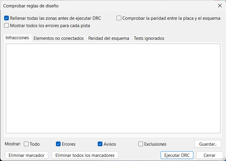
To ensure my design was correct, I closed the simulator and returned to the plate editor. I looked in the top bar for the ladybug icon with the green check to open the design rule control. Once there, I clicked on 'Run DRC'; seeing that the list of violations was empty, I confirmed that my badge had no physical errors and was ready to go into production. If there were any errors, would have used KiCad’s red arrows to fix very close tracks or missing connections
Validation of Ergonomics and 3D Virtual Prototyping
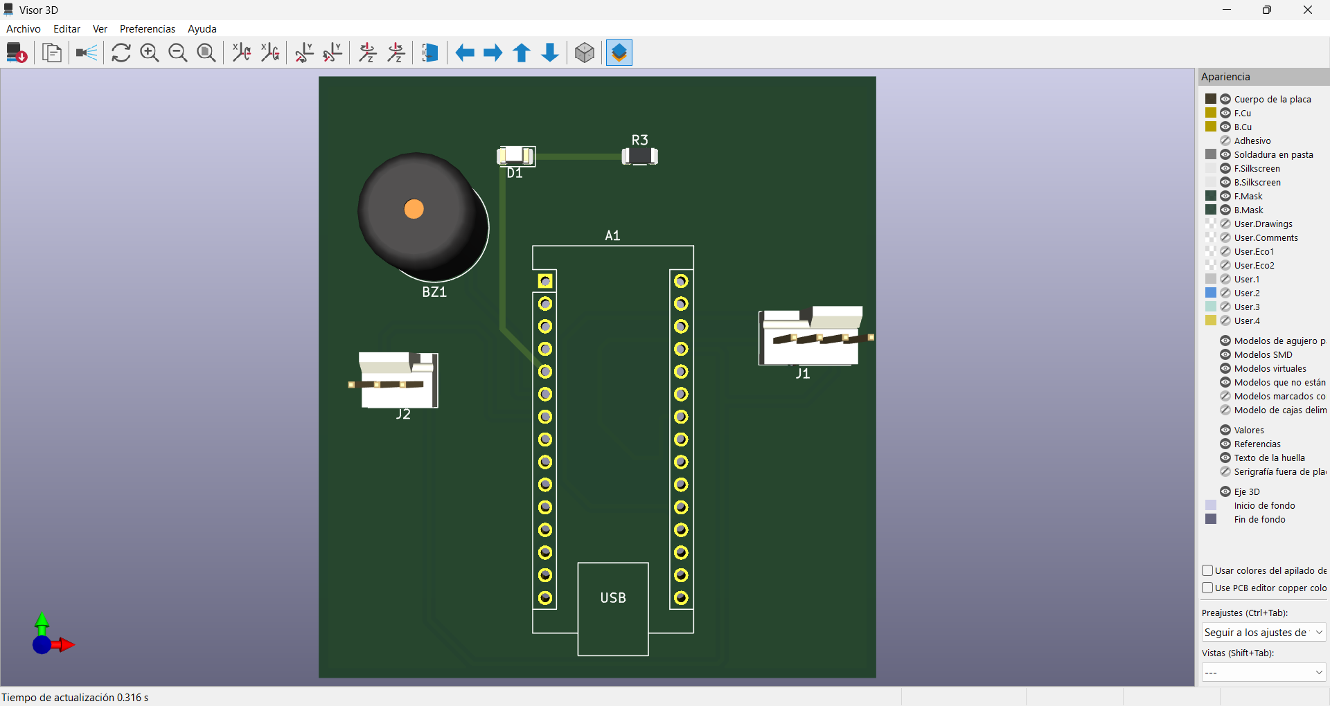
Finally, I opened the 3D viewer (as seen in the picture) to make a visual inspection of the aesthetics and ergonomics of the plate.