Electronics Design Cover

6. ELECTRONICS DESIGN

[ MISSION: HARNESS THE POWER OF ELECTRONS. ]

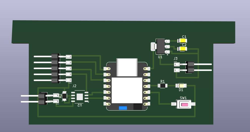
This week I worked on designing a schematic and PCB (Printed Circuit Board) for a circuit with specific functions related to my final project. For this week I decided to use KiCad because I wanted to try a new software for electronics design (since I always use Altium at school). For this project I worked with a Xiao RP2040 because we have some at the labs.

What is Electronics Design?

Electronic design is the intricate process of defining the physical architecture, components, and connectivity of electrical systems to achieve a specific functionality. In the modern era, it serves as the backbone of global innovation, bridging the gap between abstract software instructions and physical hardware execution.

[ SYSTEM_CORE: SELECT DESIGN_PROCESS ]

KICAD_MCU_CORE v6.0 FAB_ACADEMY_PROTOCOL
1. COMPONENT_LIBS
F.SilkS
2. LOGIC_SCHEMATIC
F.Cu
3. PCB_ROUTING
B.Cu
4. BOARD_GEOMETRY
Edge.Cuts
POWER_STABLE: 3.3V / GND_REF: OK

[ MISSION: LIBRARY_SETUP ]

Tutorial

Software & Library

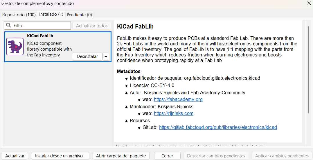
Download the official Fab Academy KiCad Library. I

  • Open Manager: Go to Tools > Plugin and Content Manager.
  • Search: Use the search bar to find specific add-ons or libraries.
  • Install: Click Install and then Apply Pending Changes at the bottom.

DOWNLOAD SOFTWARE
FAB LIBRARY

Configuration

If you want to use all the components that the Fab library has in it (which are plenty) just type Fab and click on the complement that look's like in the image.

STEP 1

[ MISSION: LOGIC_WIRING ]
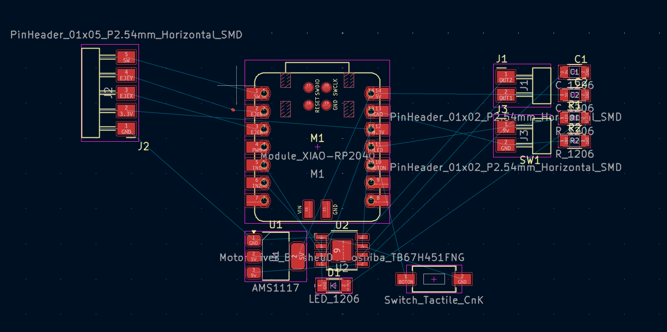
STEP 01

Placing the MCU

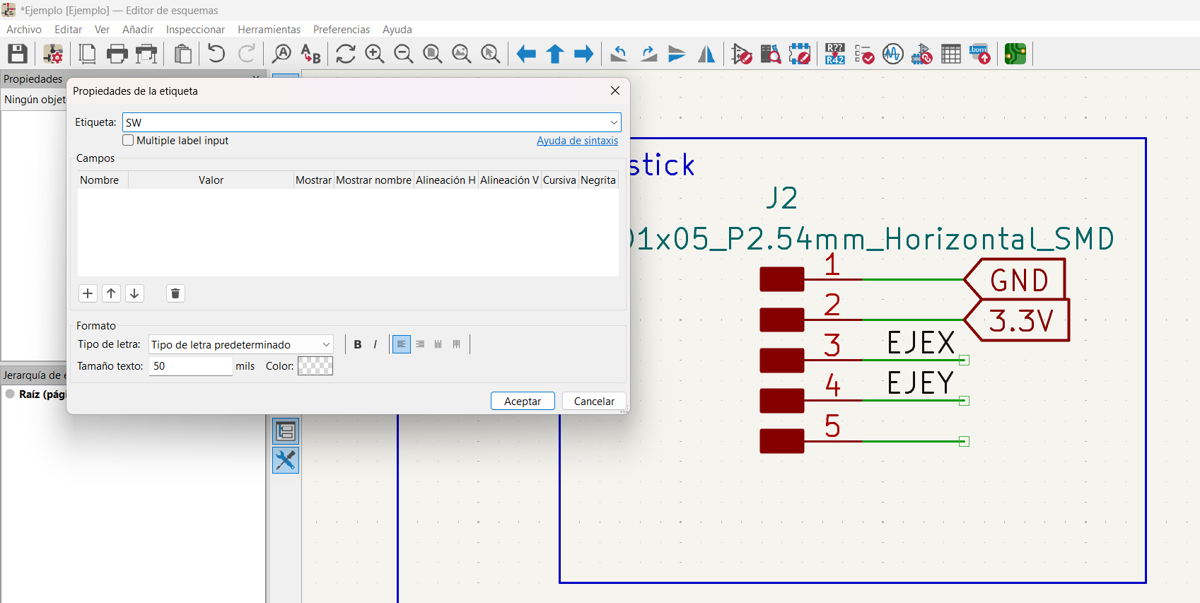
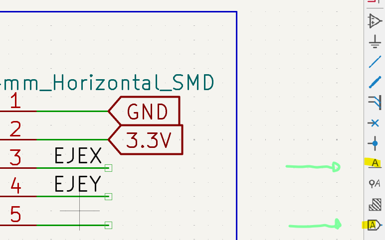
Press 'A' and search for Seeed-Xiao-RP2040. Place it in the center. Use 'W' to start wiring the pins to your components.

STEP 02

Configuration

Once the library is added, make sure to link the Footprints as well so you can visualize the components in 3D and export the board later.

ADDING LIBRARYS

Configuration

If you want to use all the components that the Fab library has in it (which are plenty) just type Fab and click on the complement that look's like in the image.

ADDING LIBRARYS

Configuration

If you want to use all the components that the Fab library has in it (which are plenty) just type Fab and click on the complement that look's like in the image.

ADDING LIBRARYS

Configuration

If you want to use all the components that the Fab library has in it (which are plenty) just type Fab and click on the complement that look's like in the image.

STEP 1

[ MISSION: COPPER_ROUTING ]

WIRING

Importing Netlist

Open the PCB Editor and click Update PCB from Schematic. Place your footprints ensuring enough space for soldering.

STEP 1

[ MISSION: PHYSICAL_LIMITS ]

Tutorial

Edge.Cuts Layer

  • Layer Selection: In the right-side menu, select the Edge.Cuts layer (yellow/gold line) to define the board's physical shape.
  • Drawing: Use the graphic tools to draw the outline. Ensure the shape is a closed loop for proper milling.
  • 3D Validation: Go to View > 3D Viewer in the top menu to verify the board's final look and cutouts.

STEP 1

[ ECAD_SYSTEM_BENCHMARK v2.0 ]

ALTIUM DESIGNER
Licensing Model Paid / Enterprise
Interactive Routing Advanced (Push/Shove)
3D Engine Native / Realistic
System Platform Windows Exclusive
> PERSONAL_LOG:
Altium is what I use at school, and it feels like a heavy-duty industrial machine. It is extremely powerful for multi-layer boards and high-speed design. However, the complexity can be overwhelming for simple prototyping, and the license restriction makes it difficult for independent makers.
KiCad 6.0
Licensing Model Open Source / Free
Interactive Routing Modern / Effective
3D Engine Raytracing Support
System Platform Cross-platform (OSX/Win/Lin)
> PERSONAL_LOG:
Trying KiCad for Fab Academy was a breath of fresh air. It is much lighter and runs smoothly on my laptop. While it lacks some of the automated "wizard" features of Altium, the community libraries and the workflow are much more aligned with the "Global Lab" philosophy. It's now my go-to for rapid PCB prototyping.

OUTPUT_STREAM: STABLE

TP_01
AND MODULE: COPPER_ARCHITECTURE +5V
Final PCB Layout

SIGNAL_ROUTING

High-integrity traces with 0.4mm clearance. Ground plane verified for EMI reduction.

TP_02
OR MODULE: PHYSICAL_GEOMETRY GND

3D_HARDWARE_VALIDATION

Interactive 3D model. Rotate and zoom to inspect component alignment and Edge.Cuts geometry.

📥

PCB and Schematics

Download the circuit that I made this week.

GET_FILES.ZIP