I carried out Characterize the design rules for your in-house PCB production process: document the settings for your machine and Document the workflow for sending a PCB to a boardhouse with my classmates, but virtually, since I am in Madre de Dios and it was difficult for me to travel to Lima. So I connected virtually with my classmates and then replicated the same process at the FAB LAB of IESTP Jorge Basadre Grohman.
Img 1
General description and use
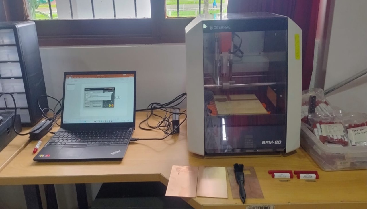
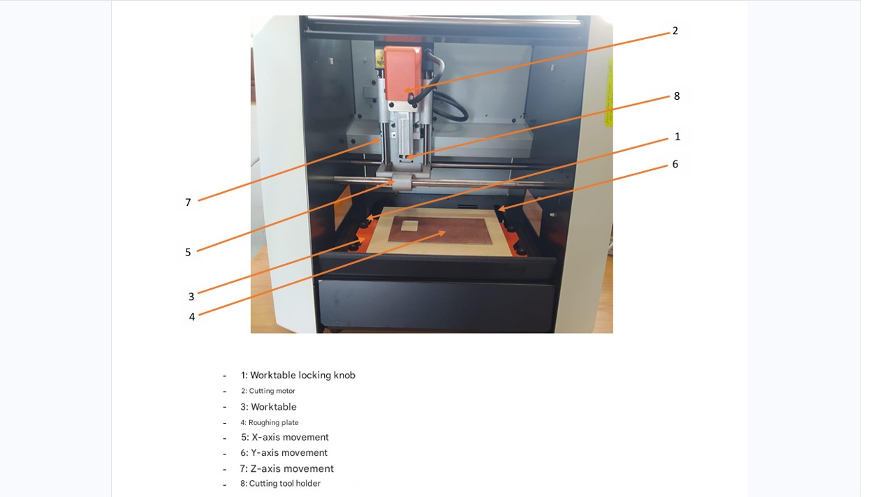
The Roland MonoFab SRM-20 is a compact desktop milling machine widely used in digital fabrication laboratories such as Fab Labs. It is designed for precision milling of small objects, including printed circuit boards (PCBs), wax molds, plastics, and soft metals. In the context of electronics production, the SRM-20 is mainly used for: PCB milling (traces and outlines), electronic board prototyping, engraving fine details on flat surfaces, and small-scale digital fabrication projects. Its high precision and ease of use make it an ideal machine for educational environments and rapid prototyping.
a) Main characteristics
The SRM-20 stands out for its precision, compact size, and intuitive interface. It operates through numerical control (CNC) and is compatible with software such as MODS and VPanel.
High-precision milling (ideal for PCB fabrication)
Compact desktop design
USB connectivity for direct control
Compatible with the RML-1 command language
Allows working with various materials such as FR1, wax, acrylic, and plastics
Easy setup and operation for beginners
The machine allows control of parameters such as spindle speed, feed rate, and cutting depth, which are essential for obtaining precise results
c) Disadvantages and limitations
Despite its advantages, the SRM-20 also presents some limitations:
Limited working area, which restricts the size of projects.
Low power compared to industrial CNC machines.
Requires manual calibration of the origin (X, Y, Z), which can cause errors if not done correctly.
It is sensitive to incorrect parameter settings, which may cause tool breakage.
Milling time can be relatively slow for complex designs.
Requires flat and well-fixed material to ensure precision.
b) Technical specifications
Specification
Detail
Model
Roland MonoFab SRM-20
Machine type
Desktop CNC milling machine
Working area (X × Y × Z)
203 × 152 × 60 mm
Maximum spindle speed
~7,000 – 8,000 rpm
Resolution
0.01 mm/step
Control system
RML-1
Connectivity
USB
Compatible materials
FR1, wax, plastics, acrylic, soft metals
Power supply
AC 100–240 V
Dimensions
Approx. 451 × 364 × 402 mm
Weight
~19 kg
Img 2
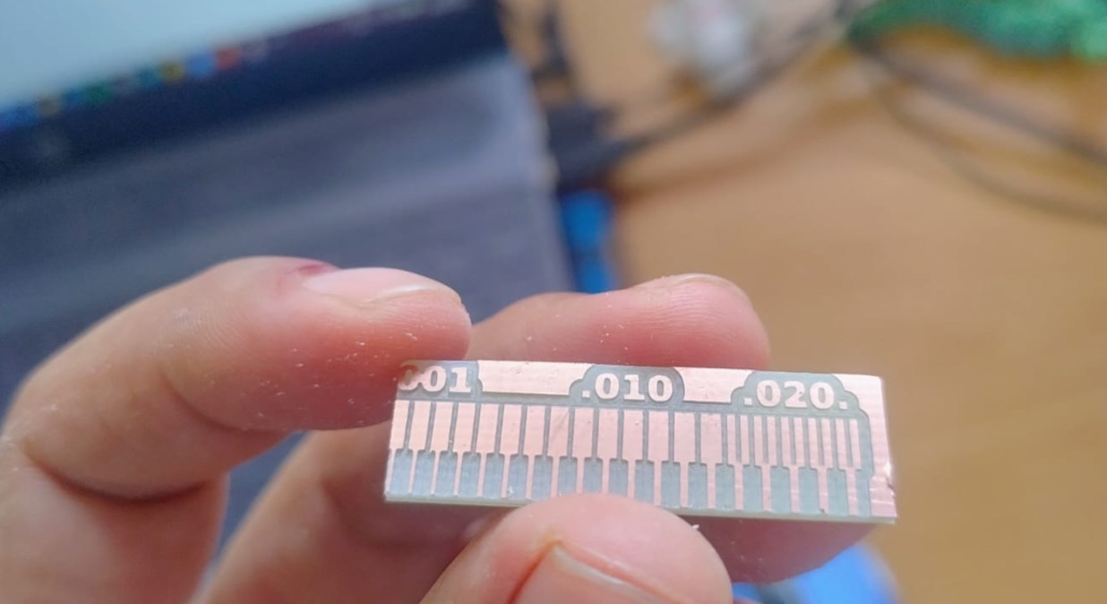
To begin with the Characterize the design rules for your in-house PCB production process, I first downloaded the files. First, the engraving of the traces must be done, and finally the cutting of the board, in order to prevent the material from moving and causing an incorrect engraving. The line test files can be downloaded here:
https://fabacademy.org/2026/classes/electronics_production/index.html
Img 3
During the manufacturing process of the printed circuit board (PCB) on the Roland MonoFab SRM-20, two end mills were used. The first was a 1/64" (0.4 mm) end mill, used to engrave and isolate the copper traces due to its small diameter and greater precision. The second was a 1/16" (1.59 mm) end mill, used to cut the outline of the PCB because it is stronger and suitable for making deeper passes through the board material.
The following shows the workflow that we followed in the Fab Lab when using the milling machine. We start from the basis that the trace files (files.rml) have already been generated previously.
VERY IMPORTANT: The milling machine must always be operated by only one person at a time, to avoid the spindle starting due to a command from one person while another person is manipulating it.
We turn on the milling machine using the power button located on the top of the machine and start the VPanel SRM-20 application on the computer.
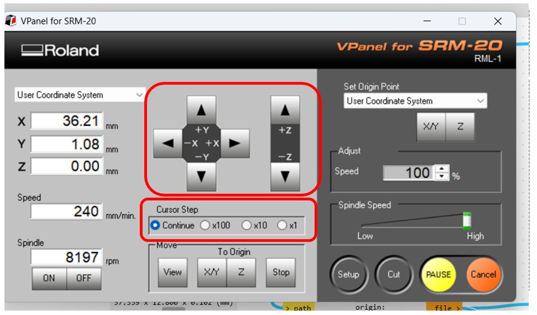
We verify the connection between the milling machine and the computer, and check that the machine moves correctly by manually moving the head along the X, Y, and Z axes. At this stage, it is essential to be very careful with the movement scale to avoid the spindle crashing into any object.
There are three movement scales: x1, x10, and x100, where each click moves the head by the indicated number of steps, with 100 steps being equivalent to 1 mm. There is also a continuous mode, in which the head moves while the button is held down. This option is not recommended for the Z axis, since it moves too fast.
Img 5
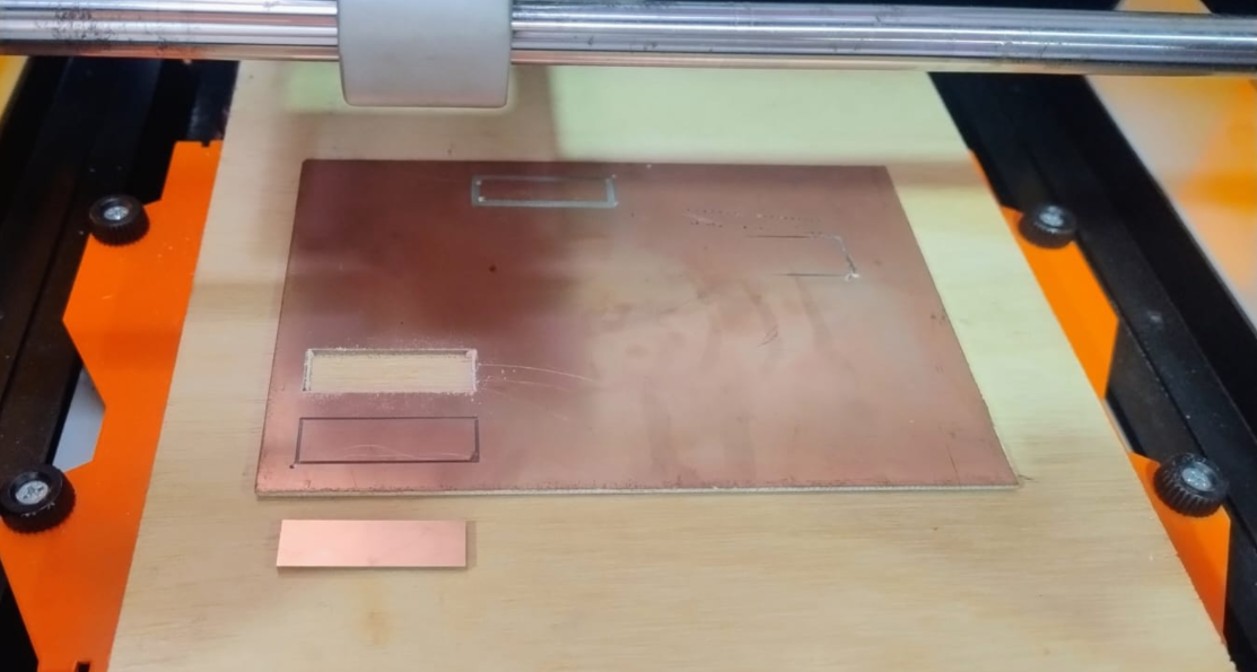
We prepare the working material by fixing the copper board to the sacrificial layer of the base using double-sided adhesive tape.
We place the end mill in the spindle and fix it with the corresponding adjustment screw. At this point, we have two types of end mills to choose from:
0.4 mm for milling, which is the one we selected in this case.
1.59 mm for cutting.
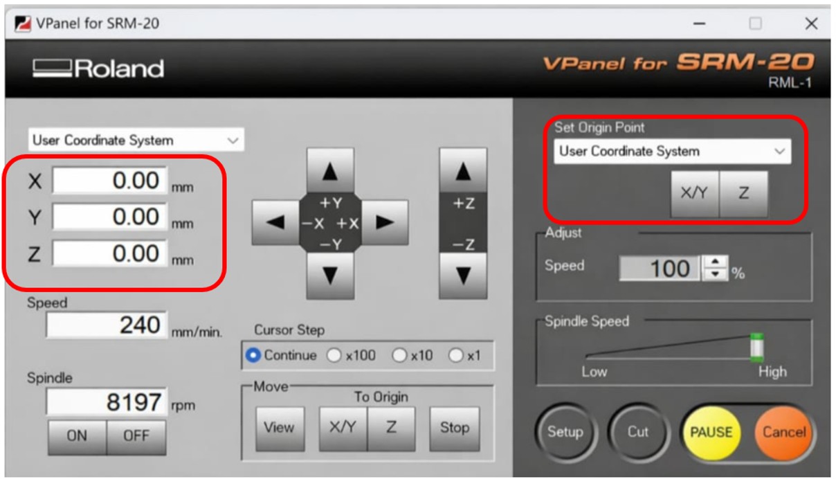
We adjust the X and Y origin position and save it by pressing Set XY Origin Point.
Img 6
We lower the drill carefully, as close as possible to the material, without touching it.
We manually adjust the height of the drill by loosening the spindle fixing screw and lowering the drill by hand until it touches the material, then tightening the screw again.
We save the Z origin position by pressing Set Z Origin.
We raise the Z axis 3 mm by pressing the manual movement button of the Z axis three times at x100 scale.
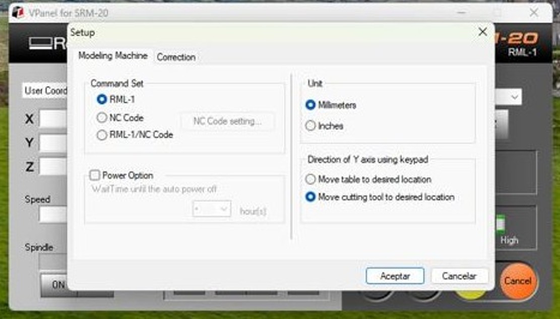
Once the origin is established on all axes, we proceed to configure the Setup software.
Img 7
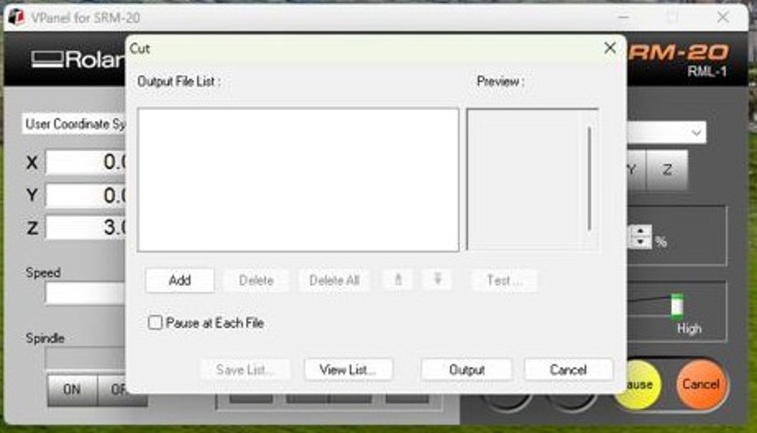
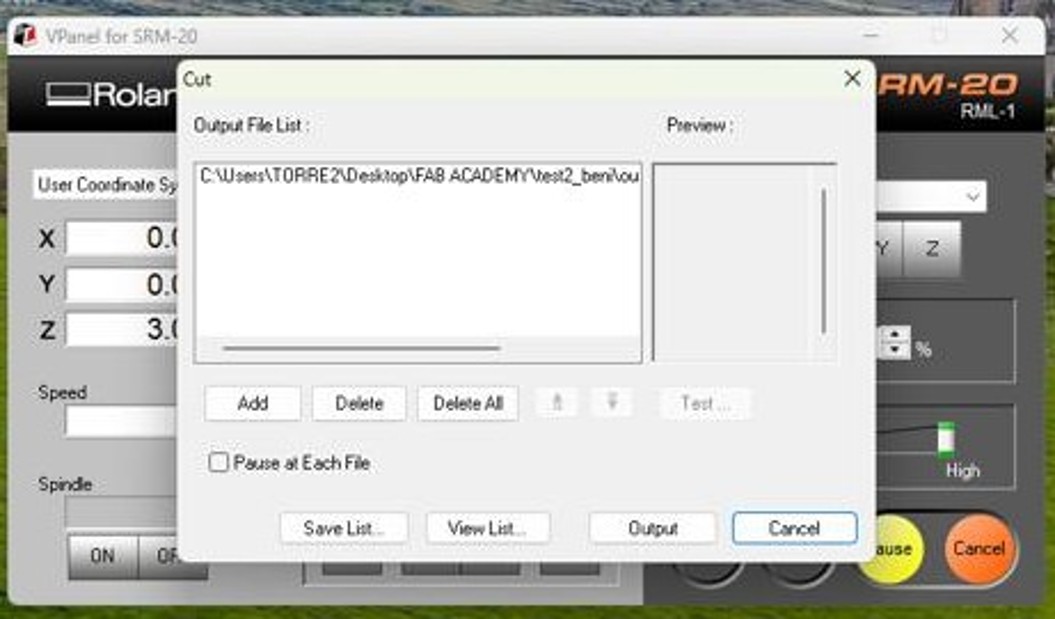
We press CUT. Important: the milling machine cover must be closed; otherwise, this step cannot be carried out.
We delete any file that may already be loaded and import our traces.rml file.
Img 8
Img 9
We press the Output button and the milling machine starts working.
At this point, it is recommended to reduce the spindle speed to 20% to check that everything is going well and, if everything looks correct, increase it back to 100%.
Once the milling machine has finished and stopped, we can press the "View" button so that the spindle moves away and the bed moves toward us, after opening the machine cover. With a vacuum cleaner, we remove the copper dust deposited on the printed circuit board and check that the result is correct.
To perform the exterior cut, we raise the spindle and change the drill for the 0.8 mm one, repeating the Z axis adjustment in the same way as before, but being very careful not to change the XY origin.
We raise the Z axis 3 mm again, close the cover, and return to the CUT menu.
We delete the previous file and import the cutting file (file.rml).
We press the Output button and the milling machine starts again. In the same way, we can initially reduce the spindle speed to 50% to make sure that everything works correctly, and then increase it again to 100%.
Once the process is finished, we press View again and, after vacuuming the area, we can remove the printed circuit board.
PROBLEMS
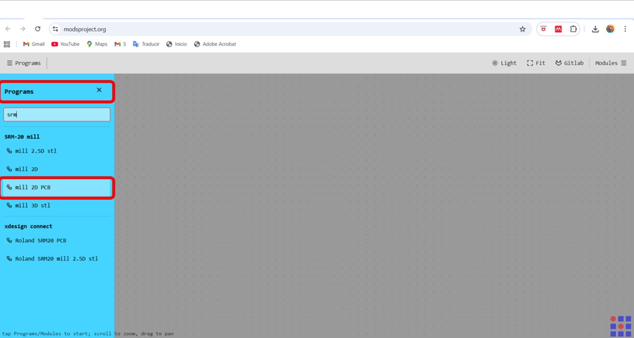
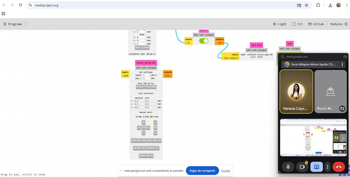
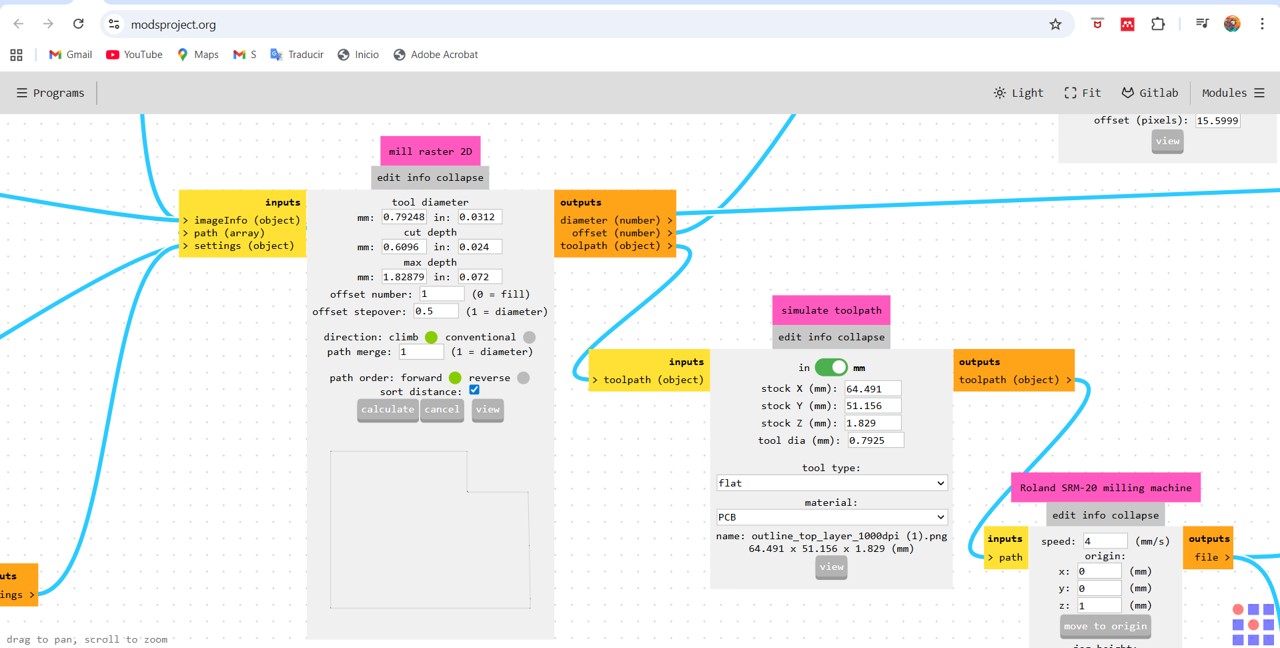
To transform the PNG image into RML I used MODS: MODS (Modular Open-Source Digital Fabrication System) is a web-based tool developed by the MIT Center for Bits and Atoms that allows controlling digital fabrication machines such as CNC milling machines. It works through connected modules that transform design files into instructions for the machine, such as RML or G-code. In the case of PCB fabrication, it is used to convert images into cutting paths, allowing the traces and the board outline to be machined precisely.
You click on programs: then in the search bar you type SRM-20 mill and select mill 2D PCB.
Img 10
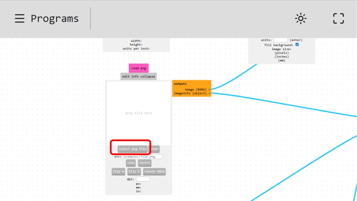
Blocks appear that must be configured. The main parts are:
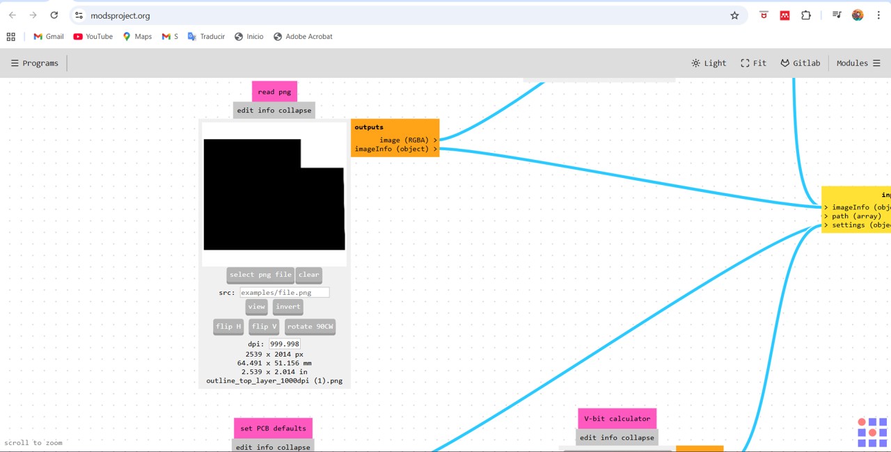
1. Read png or svg, in my case I loaded the file into read png.
Img 11
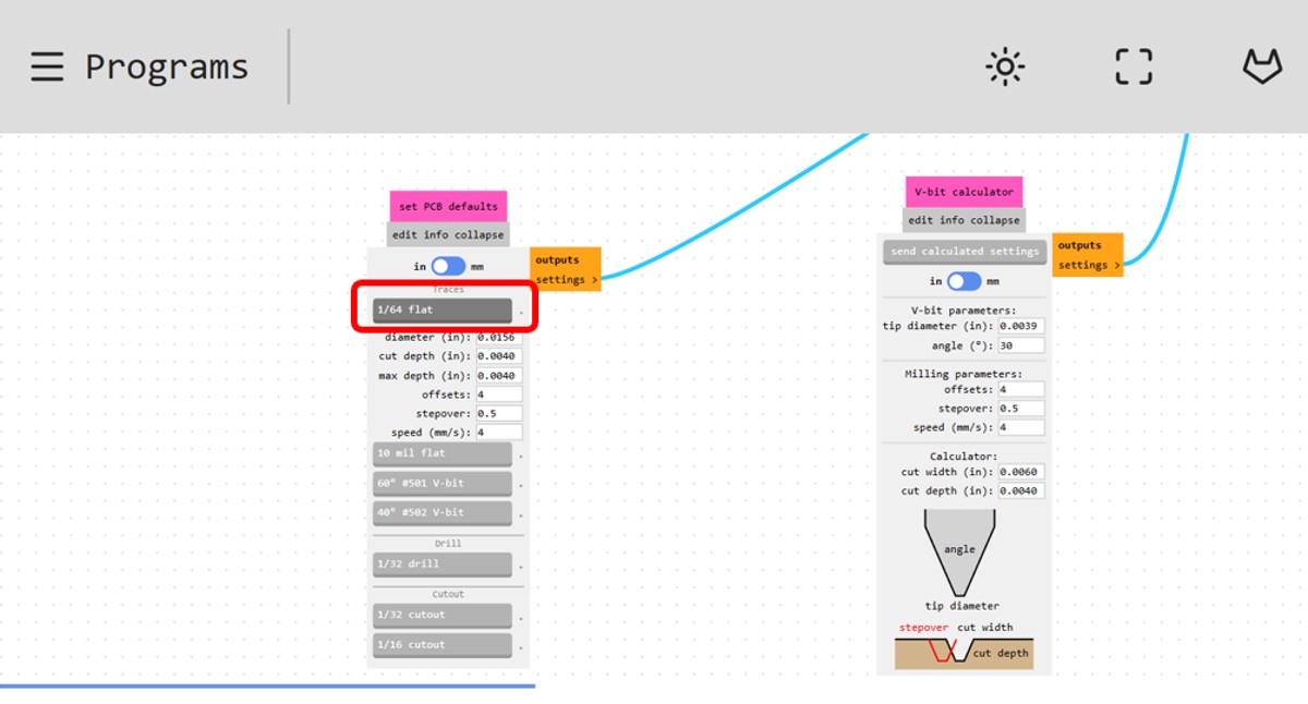
2. The other point is to choose the milling tool, in my case it was selecting 1/64 or 1/16 depending on whether it was engraving or cutting.
Img 12
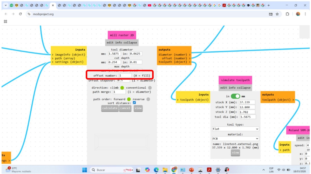
3. Then comes configuring the mill raster 2 block, here I changed the offset from 4 to 1.
Img 13
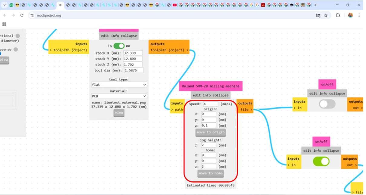
4. My problem came in this part in the Roland SRM-20 milling machine block, because I fixed my coordinates at 0,0,0 but it always started on the z axis at 60.5, until I changed it to 0.1, as shown in the image, and it worked, but it only accepts that value; any other value I enter makes the start at 60.5. Even with this configuration, the engraving stayed too high above the board and the engraving was barely noticeable, so I had to lower the end mill an extra millimeter so that it could perform the engraving.
Img 14
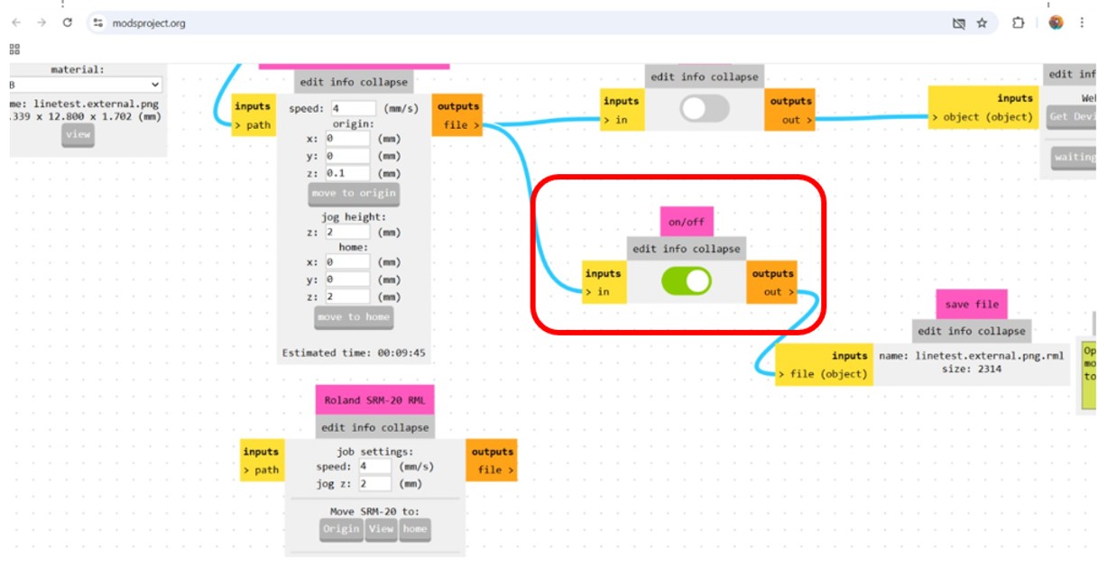
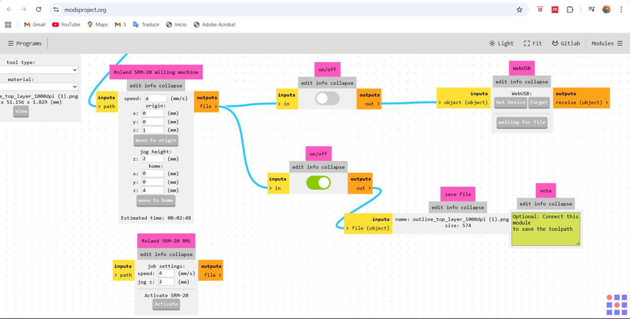
5. And finally the on/off button must be turned on so that when we press calculate the file that will be taken to VPanel can be downloaded.
6.
Img 15
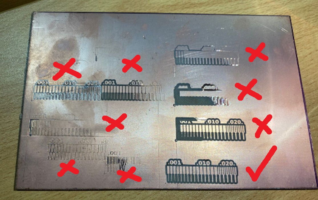
And here are the images of all the tests that I carried out.
Img 16
I met virtually with instructor Vanezza Caycho to see the problem, but it could not be solved.
Img 17
And how the engravings turned out in the various tests.
Img 18
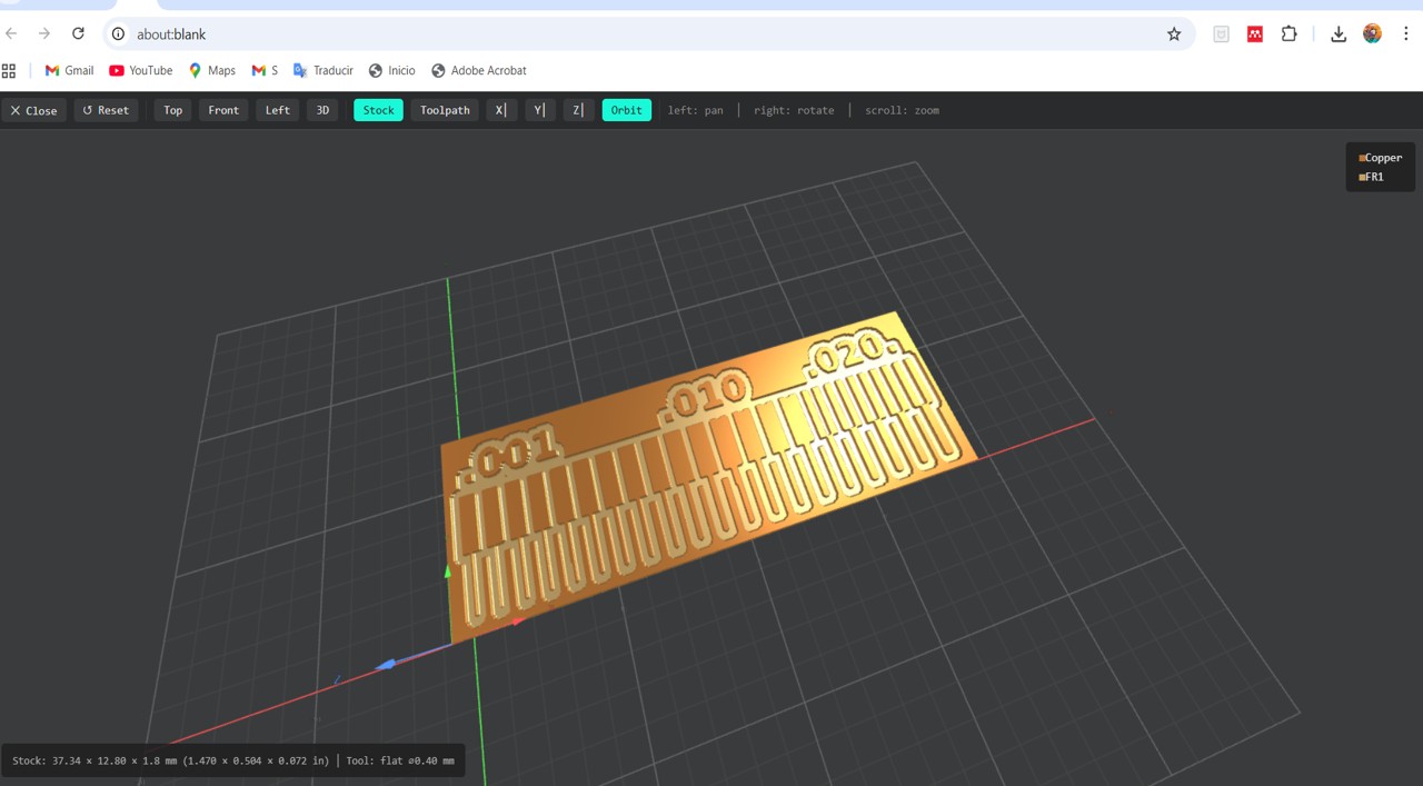
Well, after continuing to try, I managed to understand that the machine had an axis problem, and since maintenance will only be done in 3 months, I had to understand the error margins of the machine and adjust that in the origin fixing. I worked with the file created in MODS that I showed above. For adjusting the axis fixing, I made the adjustment as I mentioned before, but what I additionally did was that on the Z axis I raised it 0.2 mm and then loosened the milling bit and lowered it until it touched the board. With this, I managed to perform the engraving.
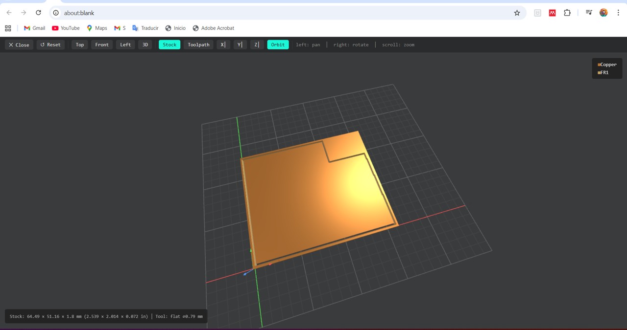
In the toolpath simulation, it could be observed like this for engraving:
Img 19
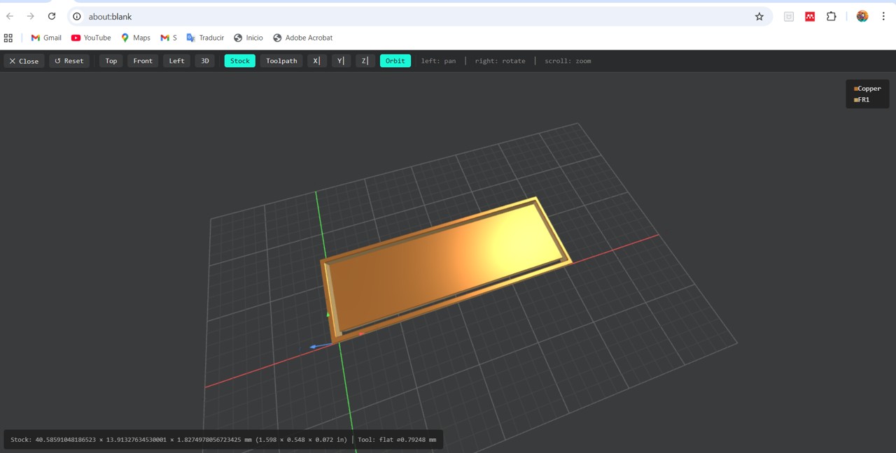
For the cutting case, for the Z axis fixing, we perform the normal fixing, then we raise and lower the milling bit until it touches the sacrificial material. With this, we achieve a correct cut.
In the toolpath simulation, it could be observed like this for cutting:
Img 20
Some cutting tests:
Img 21
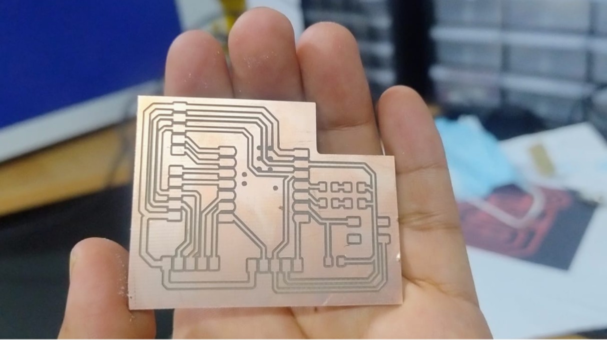
And the final piece, although I had the problem that it moved a little to the right, it turned out well, and it can be seen that the machine works well with very fine traces.
Img 22
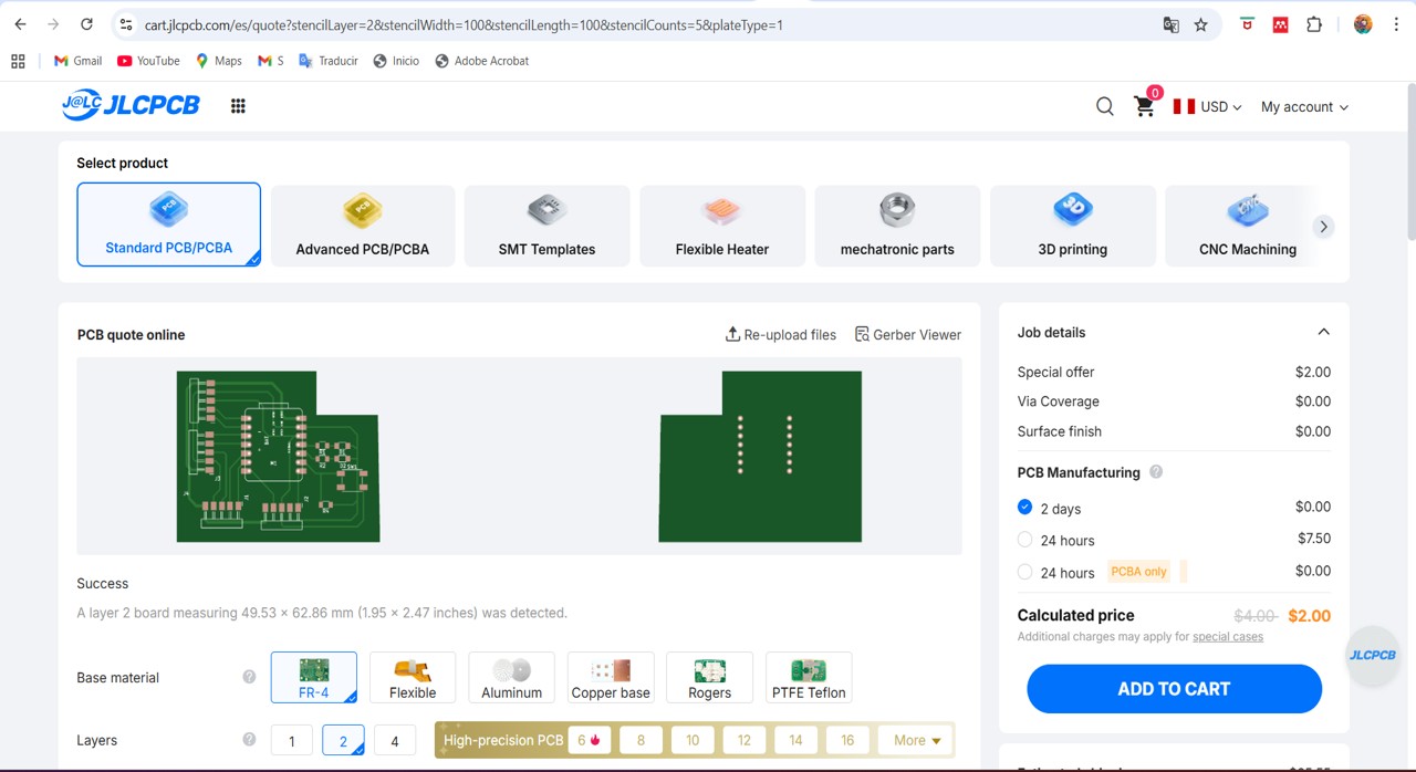
Document the workflow for sending a PCB to a boardhouse
Workflow for sending a printed circuit board to a board manufacturer.
As part of the group work, we also documented the workflow for sending a PCB design to an external manufacturer such as JLCPCB or PCBWay. Although my board was fabricated in-house, this workflow is useful for more complex designs or for boards that require vias, solder mask, silkscreen, or double-sided fabrication.
From KiCad to Gerber
1. Finish the printed circuit board design in KiCad.
Img 23
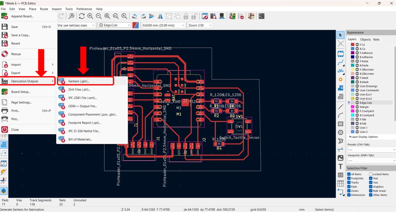
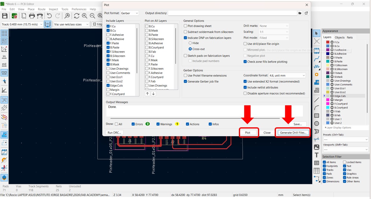
2. Open the "Plot" menu and export the Gerber files.
Img 24
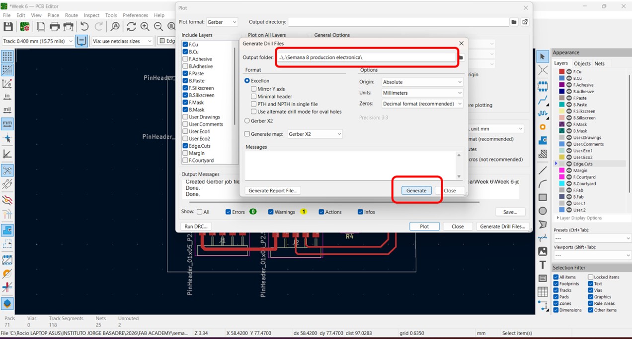
3. Also generate the drill files.
Img 25
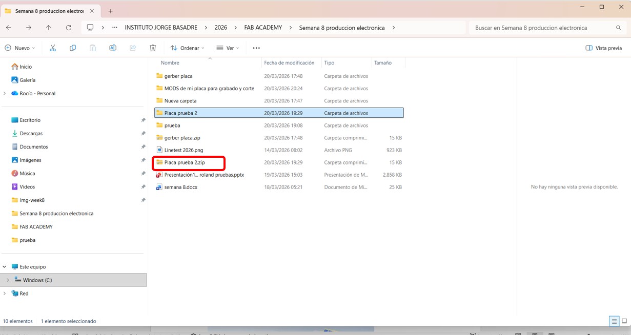
4. Save all the Gerber files and drill files in a new folder.
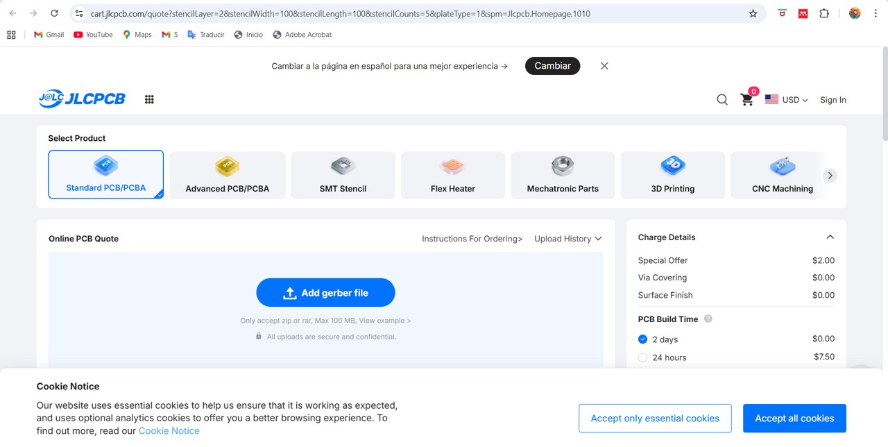
7. Upload the ZIP file to a printed circuit board manufacturing company.
Img 29
Img 30
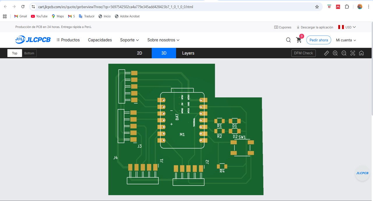
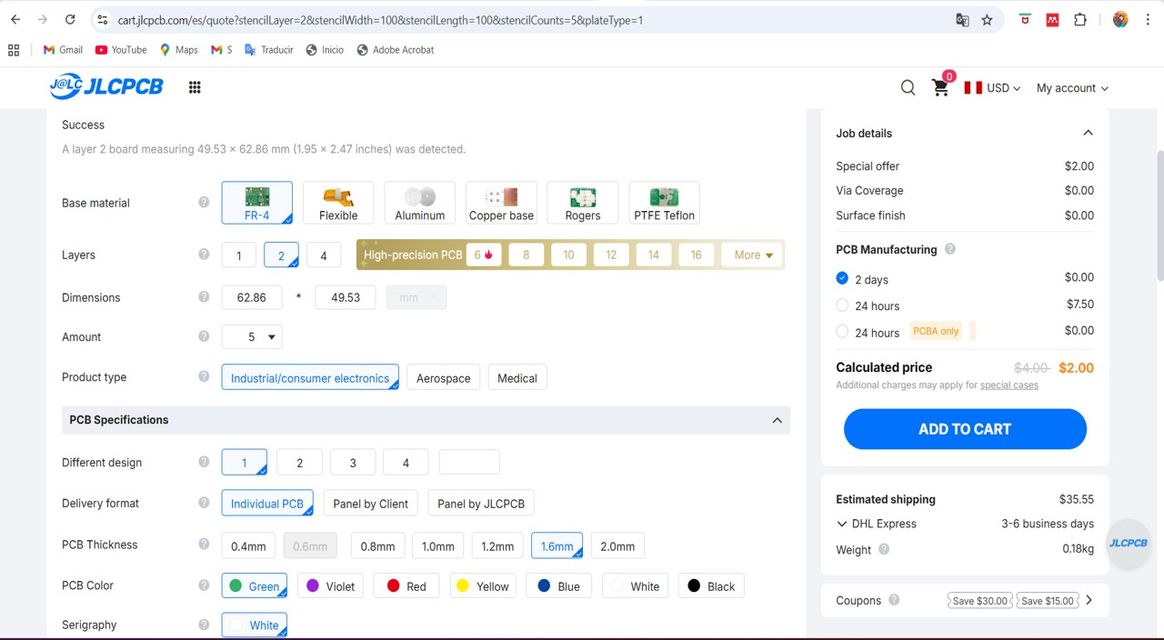
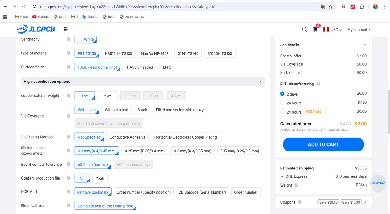
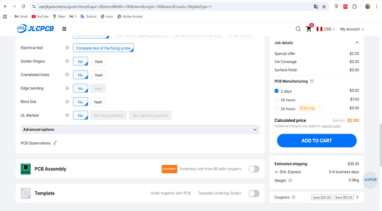
8. Select JLCPCB options.
Img 31
Img 32
Img 33
II) Individual Assignment
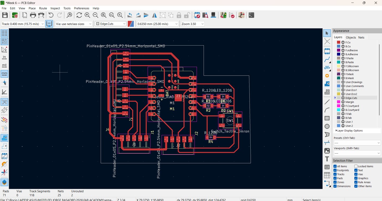
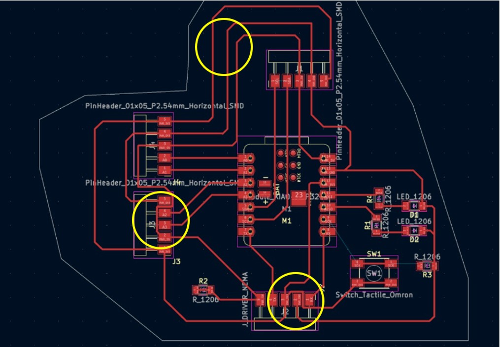
For the individual assignment, I designed and fabricated my own integrated microcontroller board. The board was created in KiCad in week 6, but I had to make a new distribution because the traces were very long and some tracks were crossing each other.
This is how my design looked in week 6.
Img 34
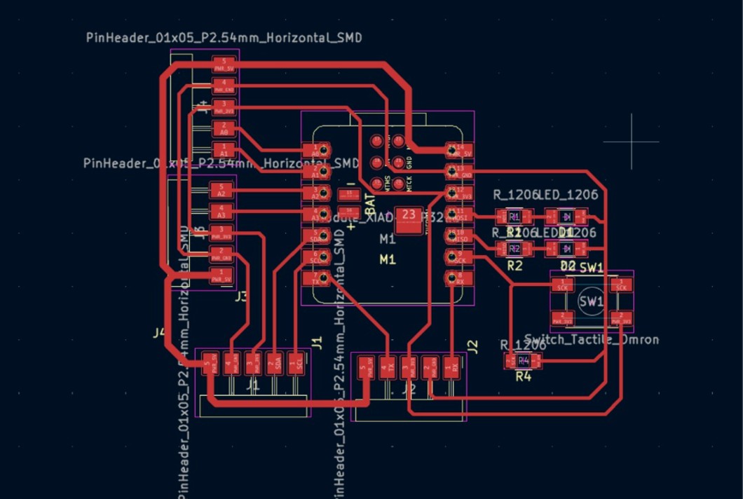
Now, after the adjustments, I changed to this new distribution.
Img 35
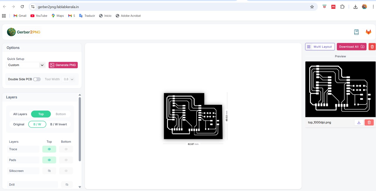
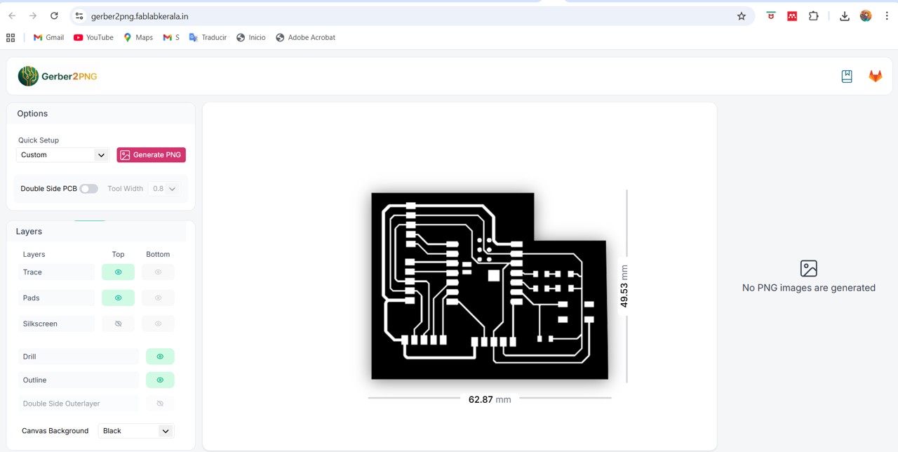
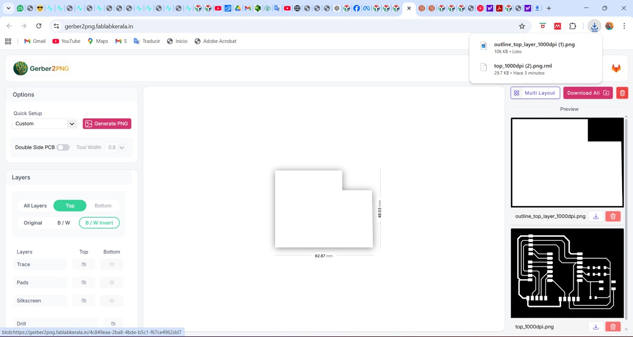
As before, I obtained the plot and drill files (if any) directly from KiCad. Then I processed the compressed .zip file with the Gerber 2 PNG application:
Link here.
In this application the zip file is uploaded.
Img 36
For engraving I used this configuration.
Img 37
For cutting I used this configuration.
Img 38
After obtaining the .png files: one for the traces and one for the outline. These are the files that I later used to configure the milling process in the MODS application.
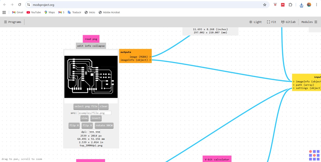
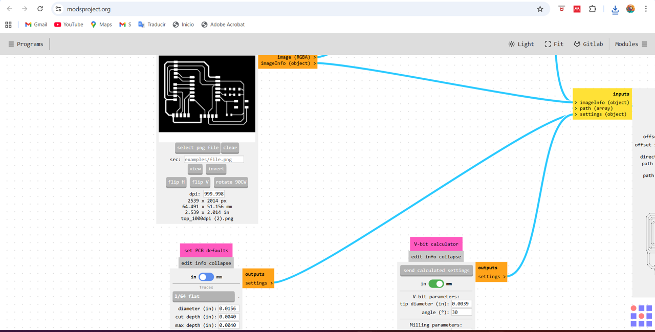
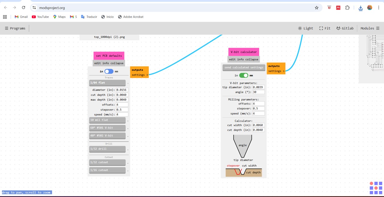
For the engraving case this is the MODS configuration that I used.
Img 39
Img 40
Img 41
Img 42
Img 43
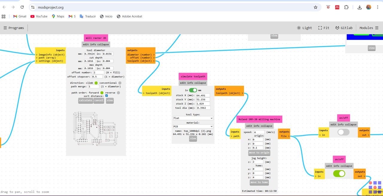
For the outline case this is the MODS configuration that I used.
Img 44
Img 45
Img 46
Img 47
Img 48
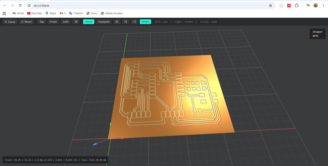
Then I sent it for cutting and engraving in the mini milling machine and this was the final result.
Img 49
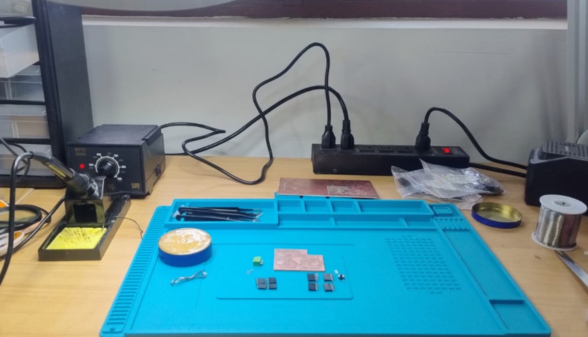
SOLDERING
Once the boards were milled, it was time to solder the components one by one. This was a very complicated task for me, since it was the first time I had soldered. I watched several videos and followed the instructions provided by my instructor Roberto Delgado.
You can review the PDF here.
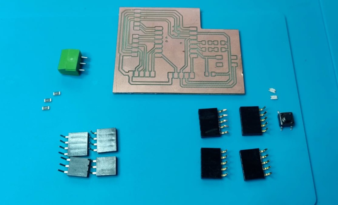
Then I carried out the inventory and search for the electronic components. In my case, these were:
A XIAO ESP32-C3 microcontroller
Pin connectors to mount and remove the controller.
A push button
Three 1 kΩ resistors
Two LEDs
Four horizontal female connectors
Img 50
Img 51
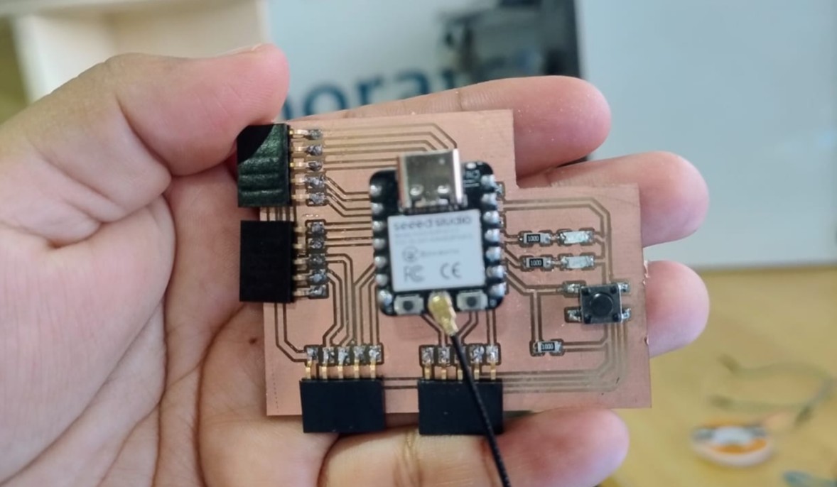
The soldering process was difficult for me. It is a tin soldering process in which, after cleaning the surfaces to be soldered and applying a small amount of flux to prepare them, both parts are heated with the soldering iron. Once hot, the solder (tin) is applied, observing how it flows and joins both surfaces. After this, the soldering iron is removed and it is left to cool so that the solder solidifies and the two parts remain joined. Soldering while holding the component with tweezers and using a magnifying glass was quite a challenge for me.
But after practicing on other boards, I think I managed it and I was excited to see if it would work.
Img 52
FUNCTIONAL TEST
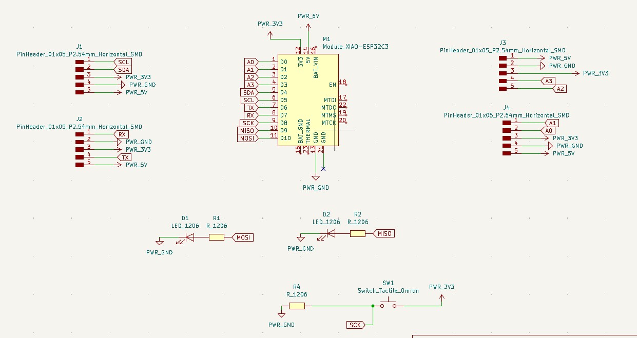
Once I had the finished printed circuit board in my hands, it was time to check its operation. First, using the multimeter in continuity mode, I checked track by track to ensure that there was continuity where it should be. At the same time, I also verified that there was no continuity between the different tracks, which means that no unwanted bridges had been created during soldering.
Once the "cold test" was completed, the moment of truth arrived: the RP2040 was connected to a power source through its USB-C port to see whether it worked or whether the only microcontroller I had would burn; it was all or nothing.
The next step was to create a program for Arduino, upload it to the controller, and check whether the rest of the board also worked. In my case, since I still do not have enough experience to write the code completely on my own, I asked ChatGPT to generate it for me. The command I used was:
“I have a printed circuit board with a Xiao ESP32-C3 controller. Please provide me with an Arduino code to make the LEDs turn on and off when the button is pressed. I am attaching the schematic of my design in KiCAD.”
Img 53
ChatGPT gave me the following code, which did work.
const int BOTON = 8;
int led1 = 9;
int led2 = 10;

void setup() {
  Serial.begin(115200);
  pinMode(BOTON, INPUT);
  pinMode(led1,OUTPUT);
  pinMode(led2, OUTPUT);
  Serial.println("Press the button...");
}

void loop() {
  int estado = digitalRead(BOTON);

  if (estado == HIGH) {
    Serial.println("leds on");
    digitalWrite(led1, HIGH);
    digitalWrite(led2, HIGH);
  } else {
    Serial.println("leds off");
    digitalWrite(led1, LOW);
    digitalWrite(led2, LOW);
  }
  delay(200);
}
Once the program was compiled, I was able to verify that the LED turned on and off every time I pressed the button.
Video 1
Reflection
During this week of electronic production, I better understood the entire PCB fabrication process, from design to assembly. One of the main challenges was correctly adjusting the milling parameters and understanding the limitations of the machine, such as axis errors, which forced me to be more precise in the origin calibration and in the Z-axis configuration.
I also learned the importance of considering the real available components from the design stage (such as resistors and packages), since this can directly affect the final assembly. The soldering process was key to improving my manual skills and understanding how small details influence the operation of the circuit.
In general, this week helped me connect theory with practice and develop better judgment to solve fabrication problems in real time.
Conclusions
It is essential to correctly adjust the machine parameters (speed, depth, and origin) to obtain good milling results.
Mechanical errors can be compensated with proper calibration and previous tests.
The design must adapt to the available components to avoid problems during assembly.
Soldering requires practice and temperature control to achieve clean and functional connections.
Validating the circuit (connections, pins, resistors) is key to ensuring that the system works correctly.
The integration of design, fabrication, and programming makes it possible to obtain a complete and functional electronic system.
Files & Downloads
In this section, the design and fabrication files used during this week are provided. These include PCB design files, MODS toolpaths, and additional files required for the milling process.


.png.rml)
.png (1).rml)
.png)
.png)