Assignment requirements
Group assignment
- Characterize the design rules for your in-house PCB production process: document the settings for your machine
- Document the workflow for sending a PCB to a boardhouse
- Document your work to the group work page and reflect on your individual page what you learned
Individual assignment
- Make and test a microcontroller development board that you designed
Progress status
Group work
Done
In-house PCB production process
Individual work
Done
Make and test a microcontroller development board
Documentation
Done
Upload .zip with source files.
1) Introduction
Huge thinks TO-DO
- Characterize the PCB fabrication
- Mill copper traces wiht the CNC machine
- Cut the board and test it
2) Group assigment - Learning how to design a PCB production process
For more details visit Fab Lab Peru Week 8 Group assignment
Hybrid exploring and application
- Lab structure
- Signs
- Warnings
3) Individual assigment
Project idea
- PCB Design - KiCad
- Generate G-Code - intructions to CNC
- Milling - V-bit engraving tool
- Drill and cut

Reviewing design
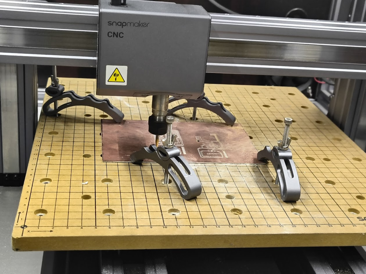
Milling at CNC
Milling at CNC
PBC final product
PBC final product
Design 2 with Fusion
Review design 2 at Lab
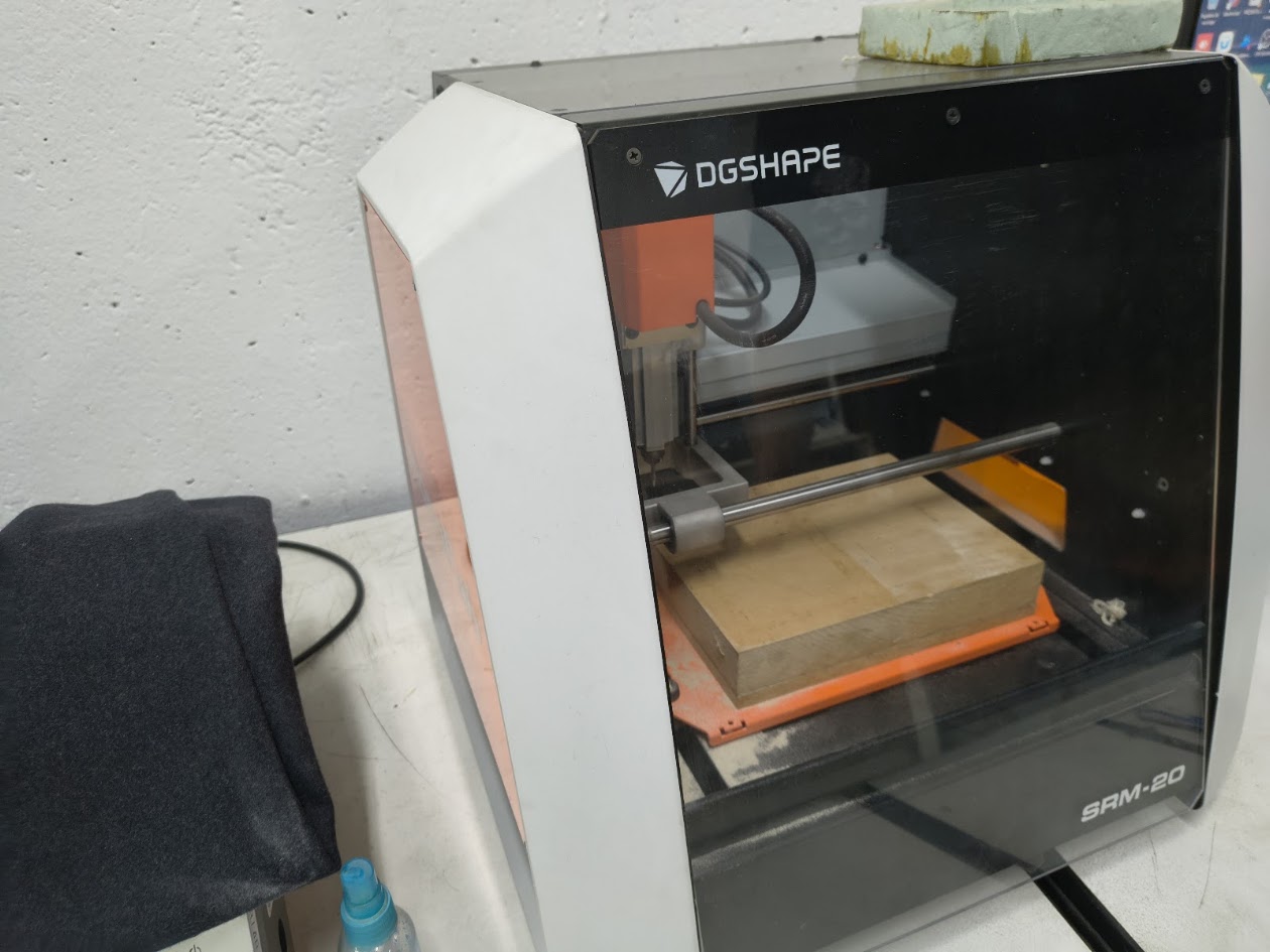
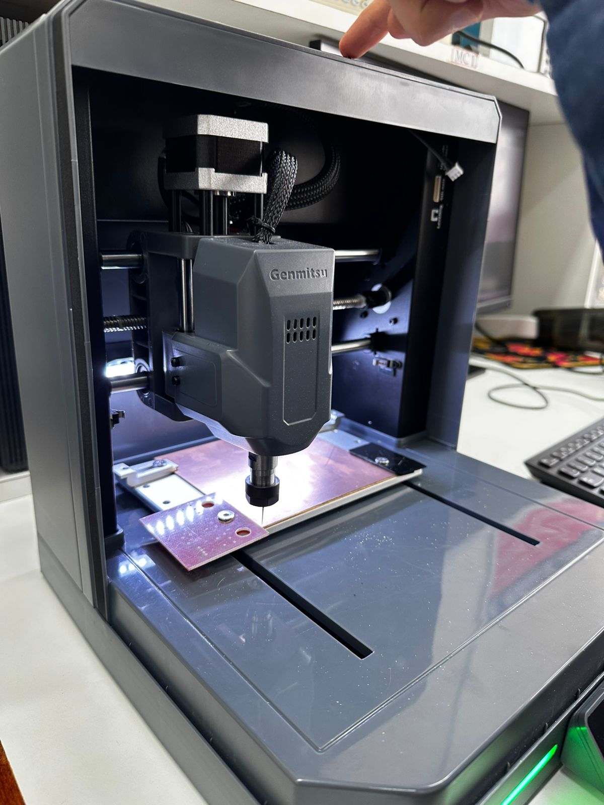
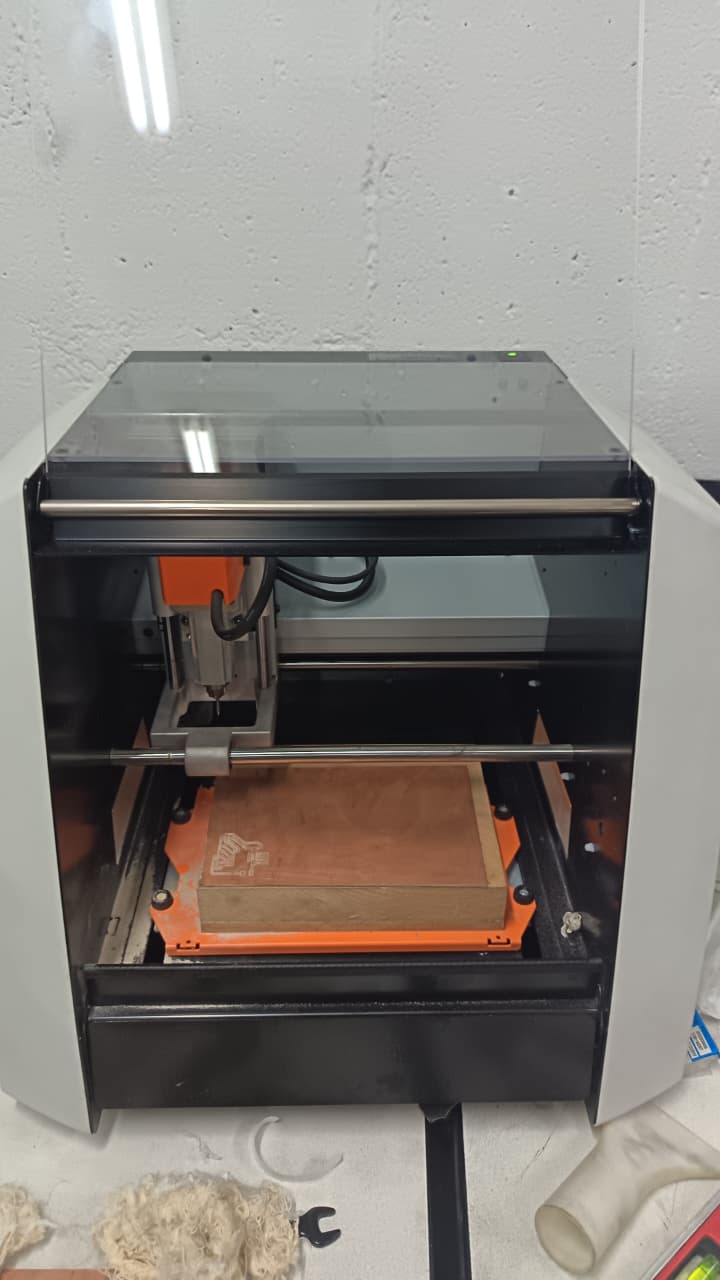
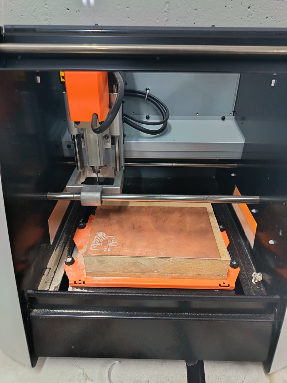
Milling the design 2. we used a MonoFab SRM-20. It is a desktop CNC machine
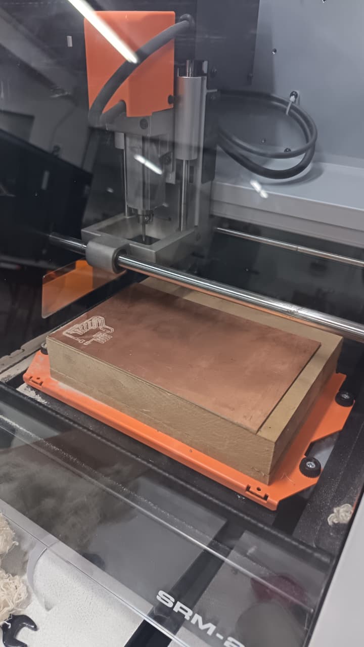
The MonoFab SRM-20 is adequate for small-scale production and versatile with a wide range of materials.
We used a 1/32 milling cutter for milling the design 2. It is a 0,79 mm diameter cutter, suitable for precise cuts in electronics boards - PCB (Printed Circuit Board) milling process
The calibration of the CNC machine is crucial for achieving precise results in PCB milling.
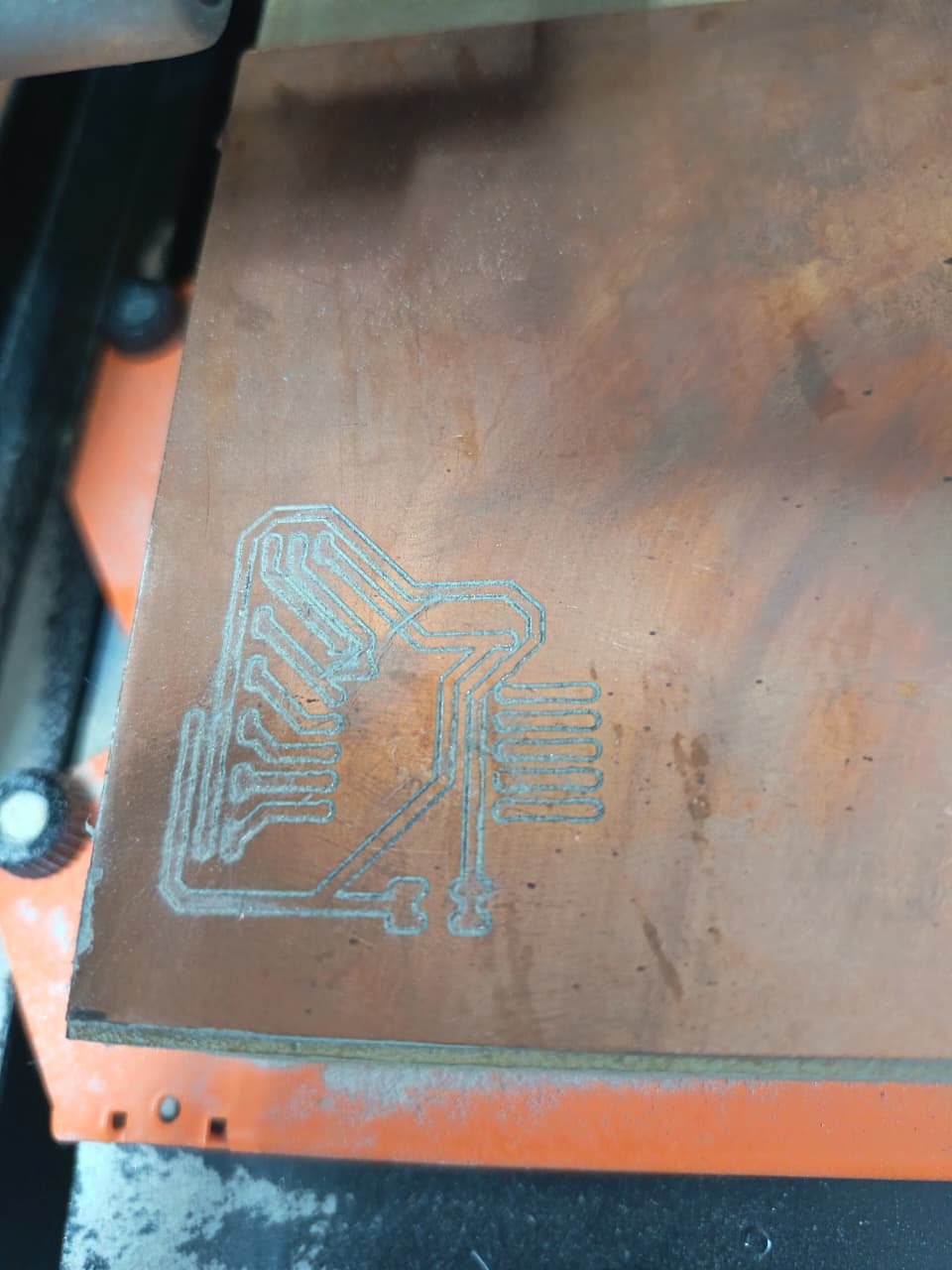
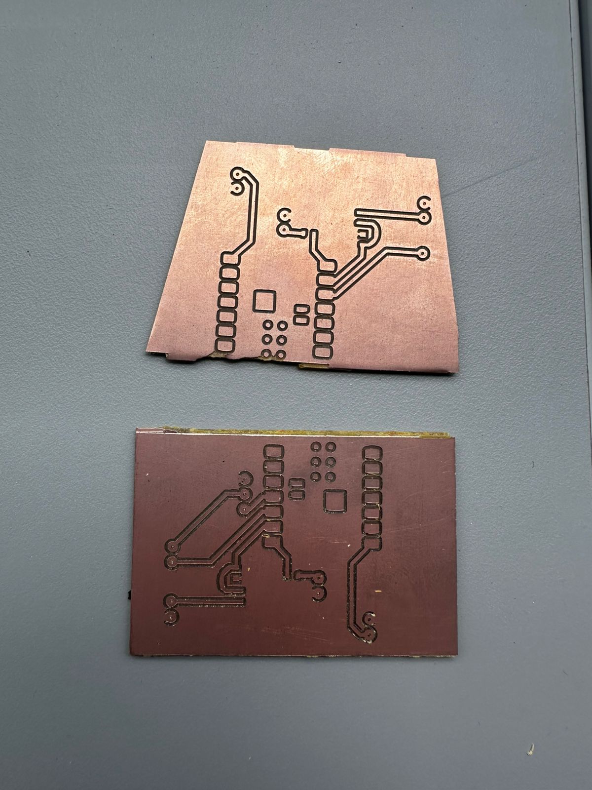
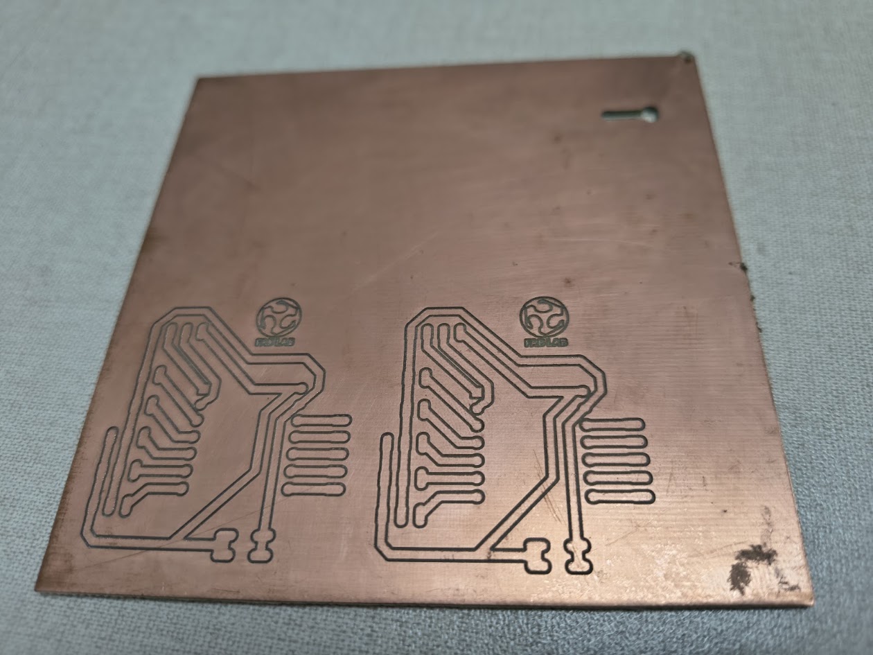
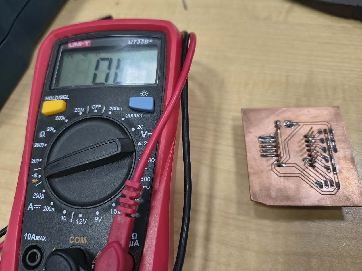
PCB Milled
Reviewing the product
Accesories
During this procees, we milled four Design 2 - PCBs on the MonoFab SRM-20, because we didn't know all the conditions and we were learning this new topic

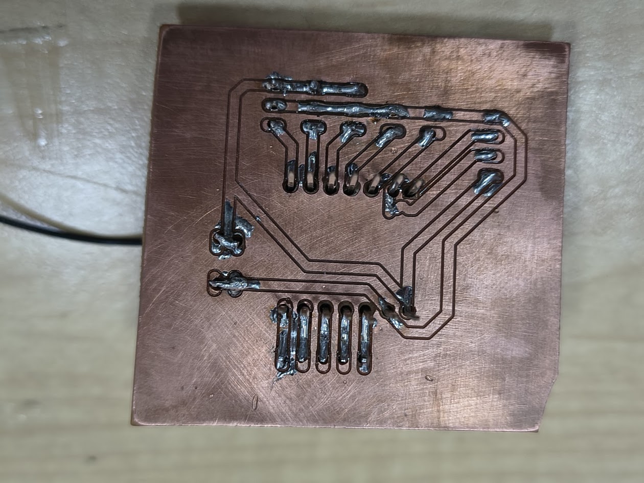
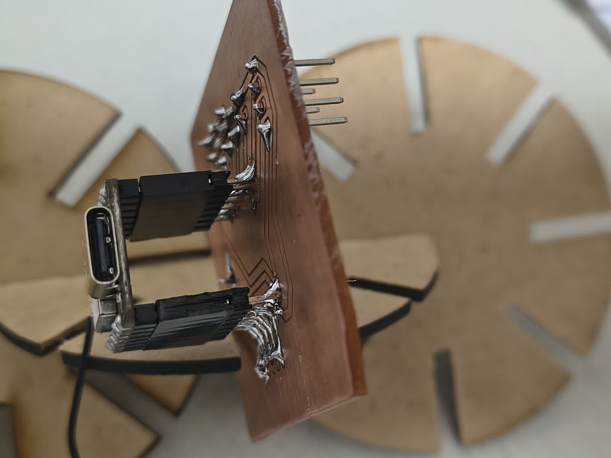
This is an operative PBC but we drilled and welded the sprats in the back. We were testing the design
This is another operative PBC but we drilled, welded the sprats and make a mistake with the Xiao ESP 32 C3 routes
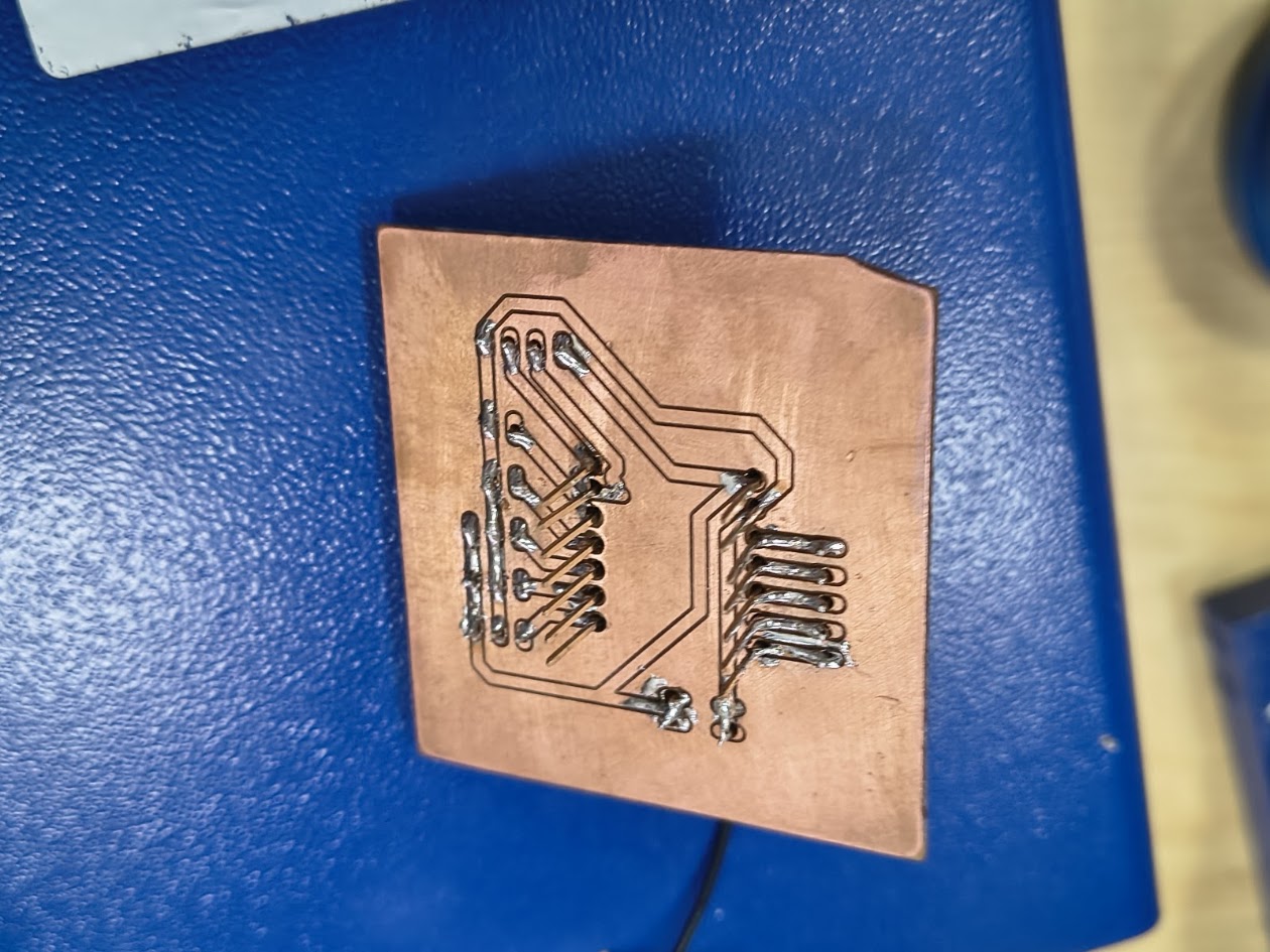
Reviewing PCB. An ungly weld

Reviewing routes and welds
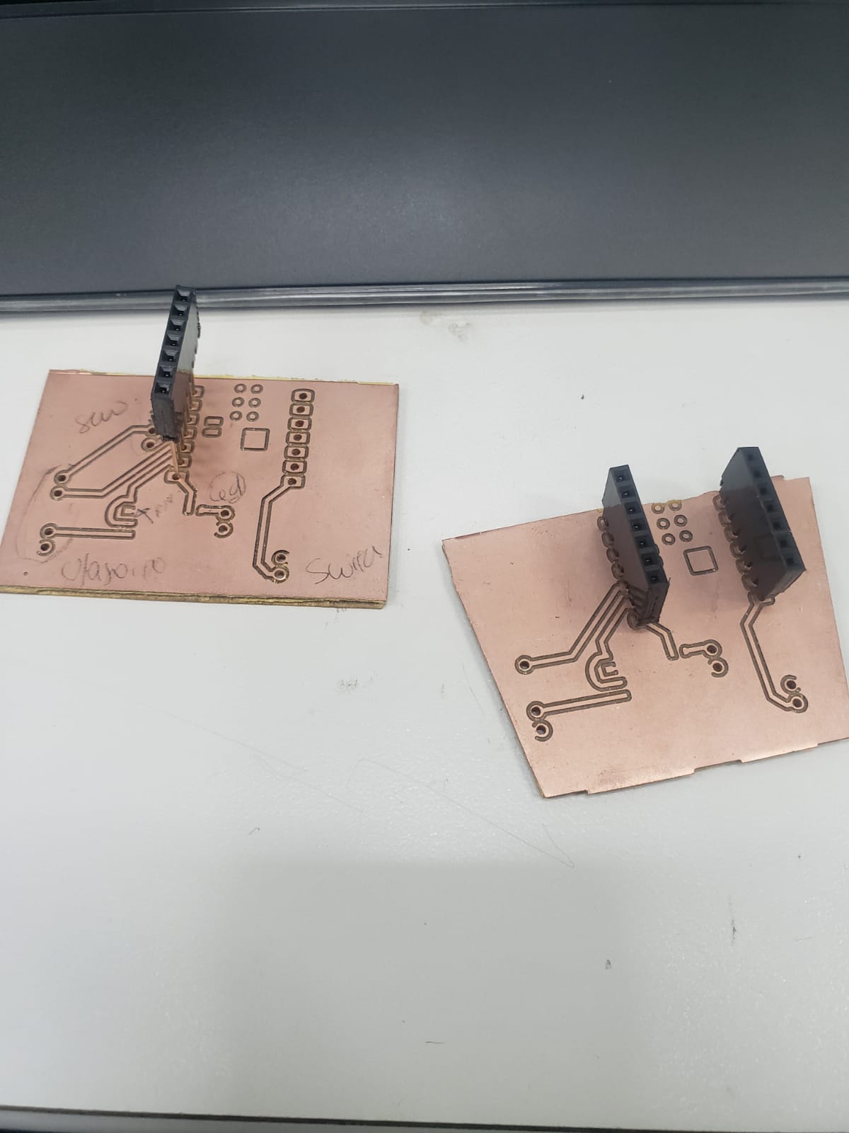
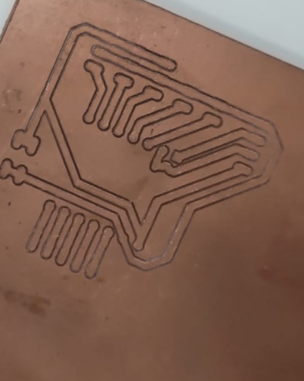
PCB during this learning process, not drill - desing 1
PCB during this learning process, not drilling in and incorrect face- desing 2
PCB during this learning process, not drilling - desing 2
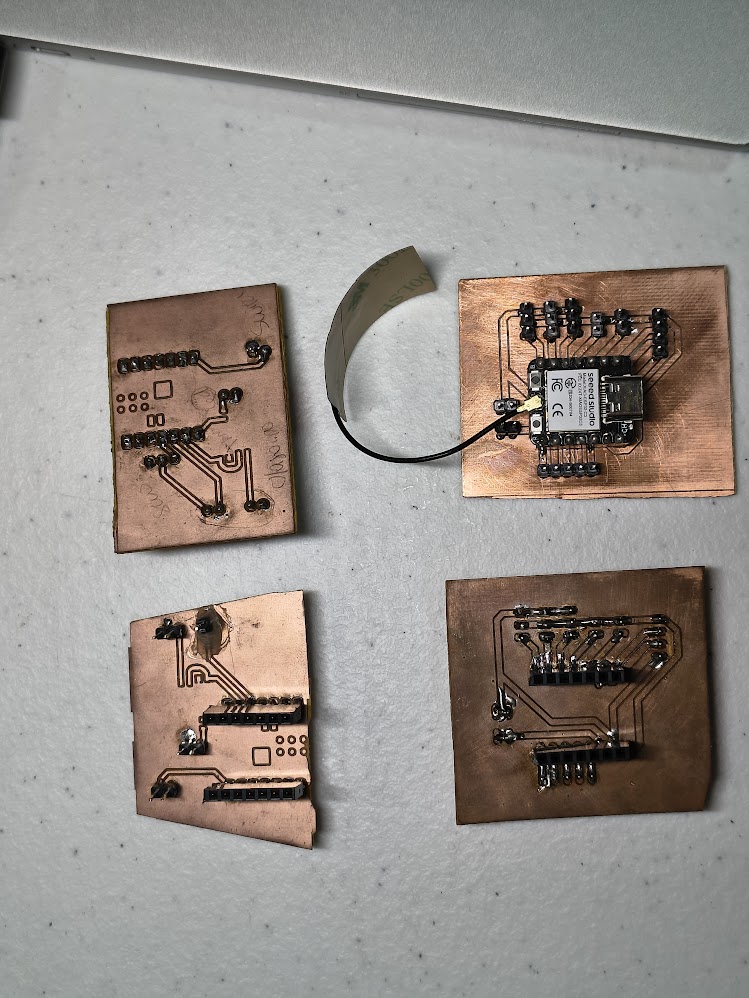
PCB during this learning process - Desing 1 & 2
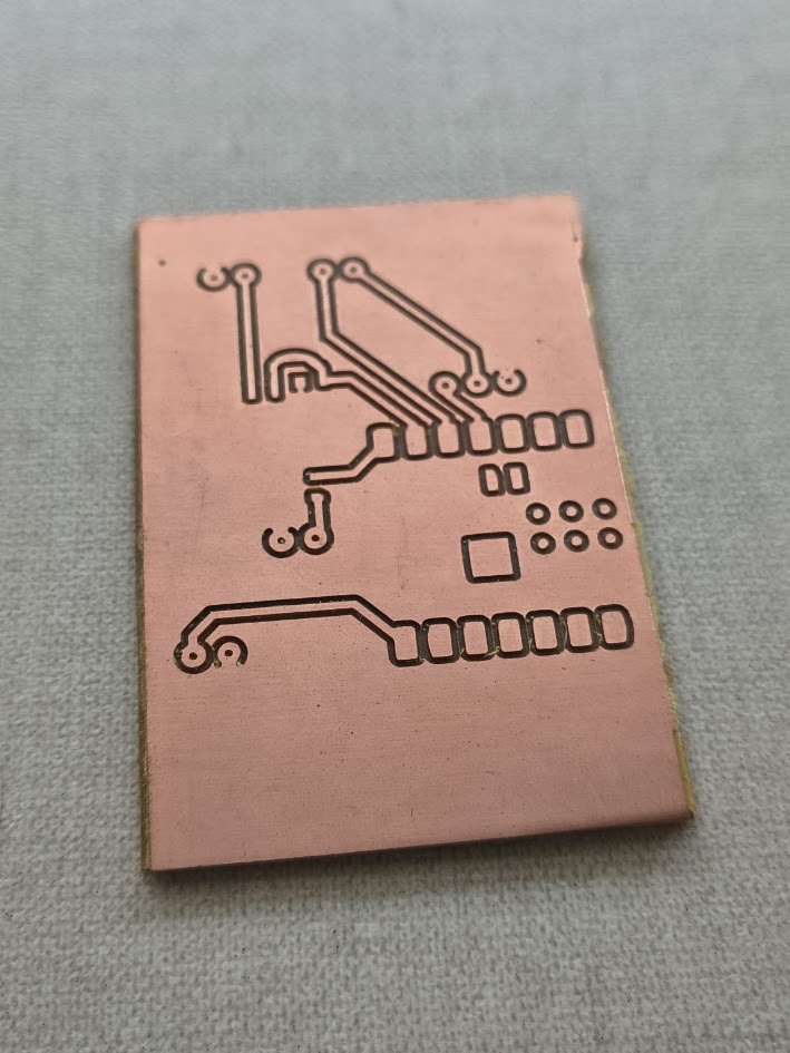
PCB final - the last version - desing 2 final
Milling at PUCP CNC
3.1) Additional individual assigment
Project production
- Show schematic and PCB layout images
- Clear labeled schematic
- Explain microcontroller pins and connections (VCC, GND, I/O)
- Schematic - PCB - Export - Fabrication files (screenshoots)
- Preparation for production: export settings
- File for preparation for milling
- Soldering /stuffing documentation

This additional assignment, we worked on Fab Lab UNI
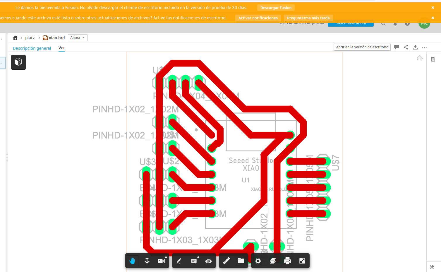
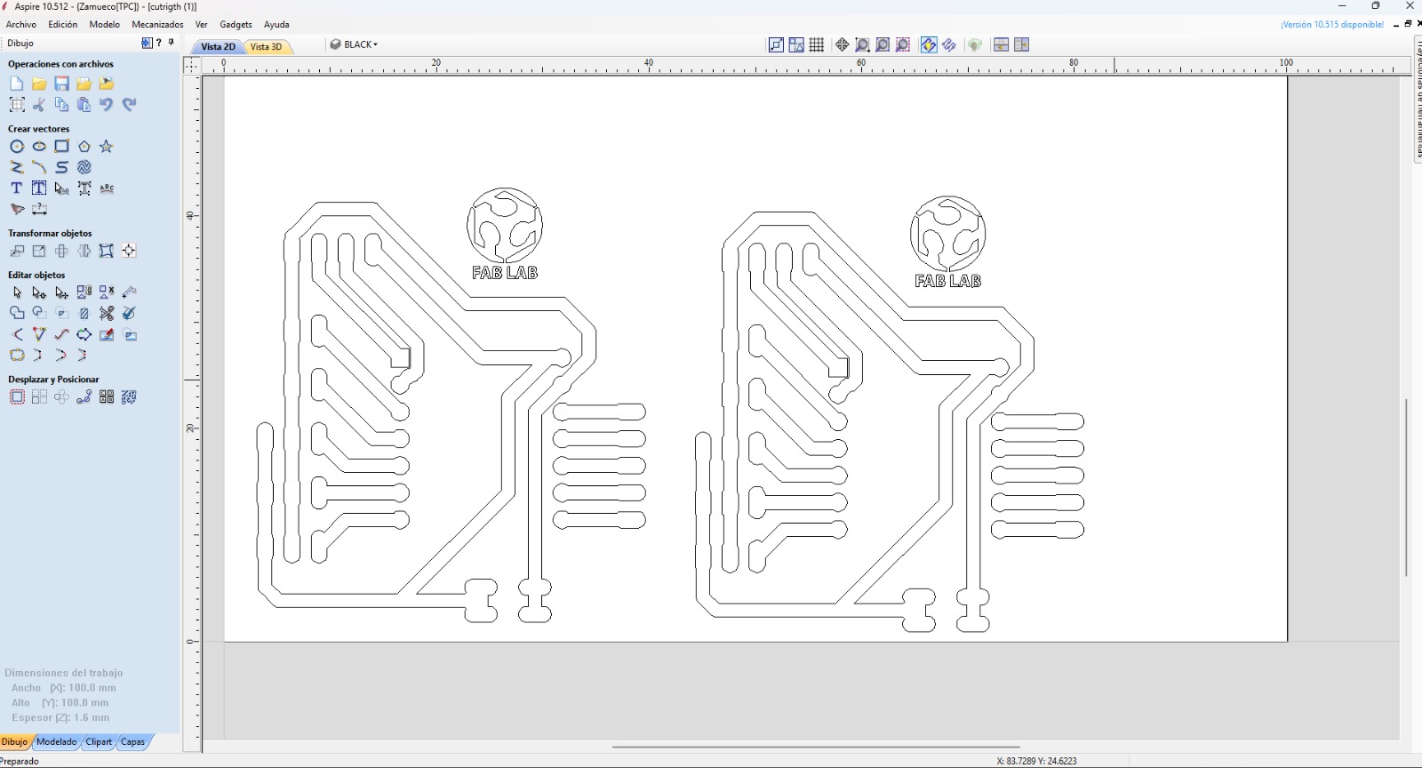
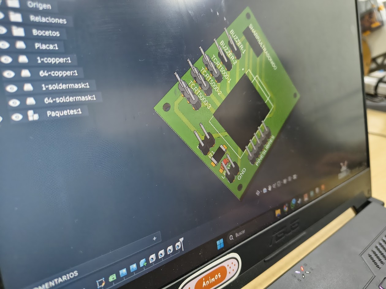
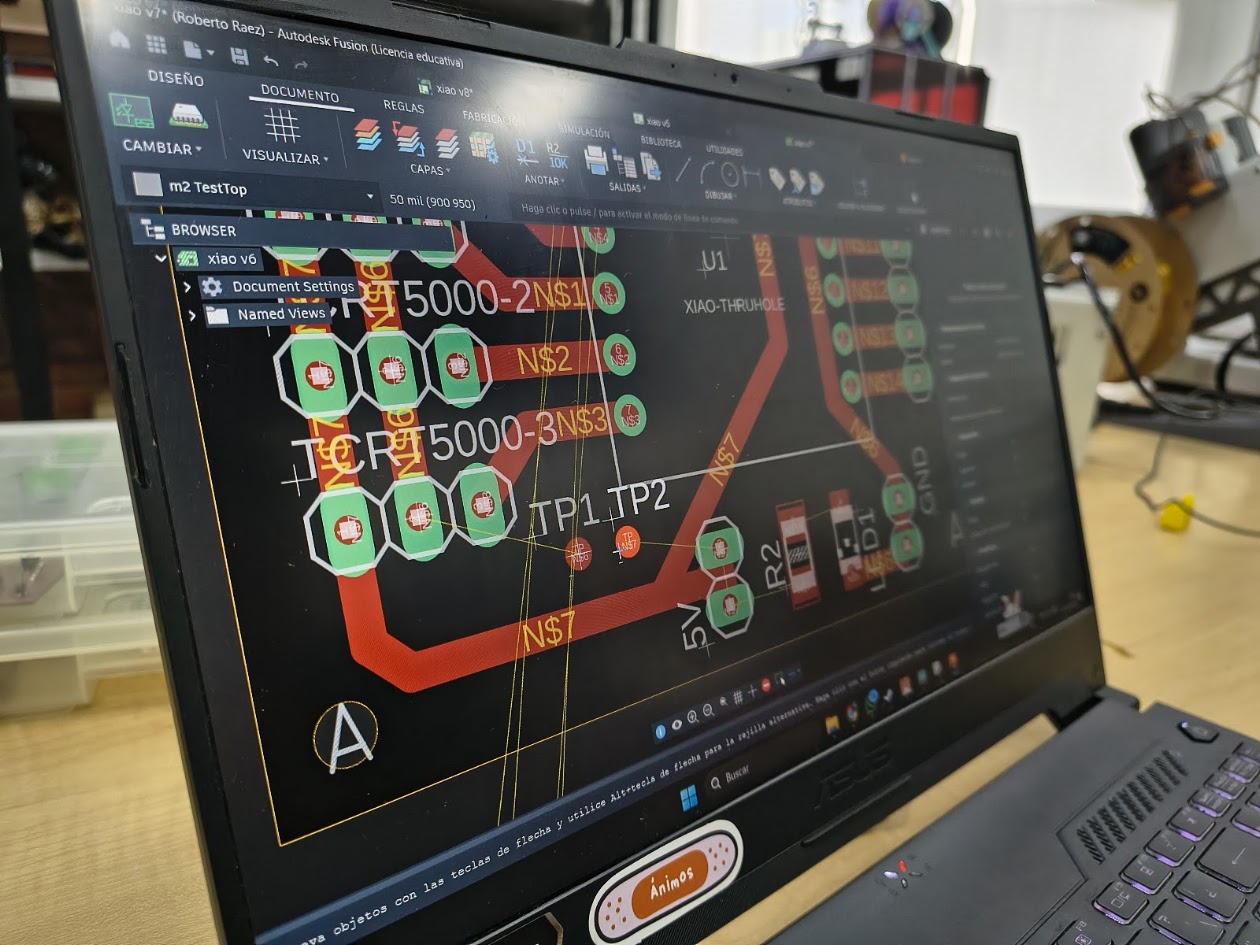
Design: PCB layout on Fusion 360 with connections
Design: PCB layout on Fusion 360 screenshot
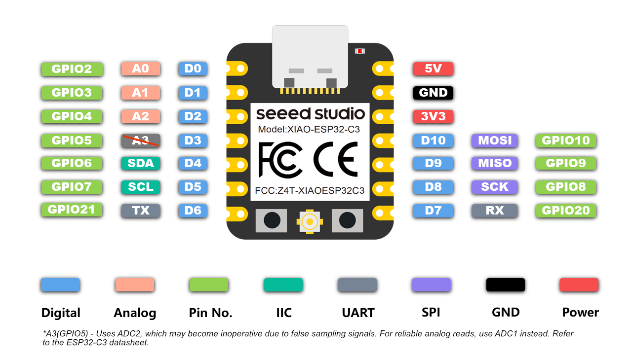
Design references: Microcontroller pins and connections https://wiki.seeedstudio.com/XIAO_ESP32C3_Getting_Started/
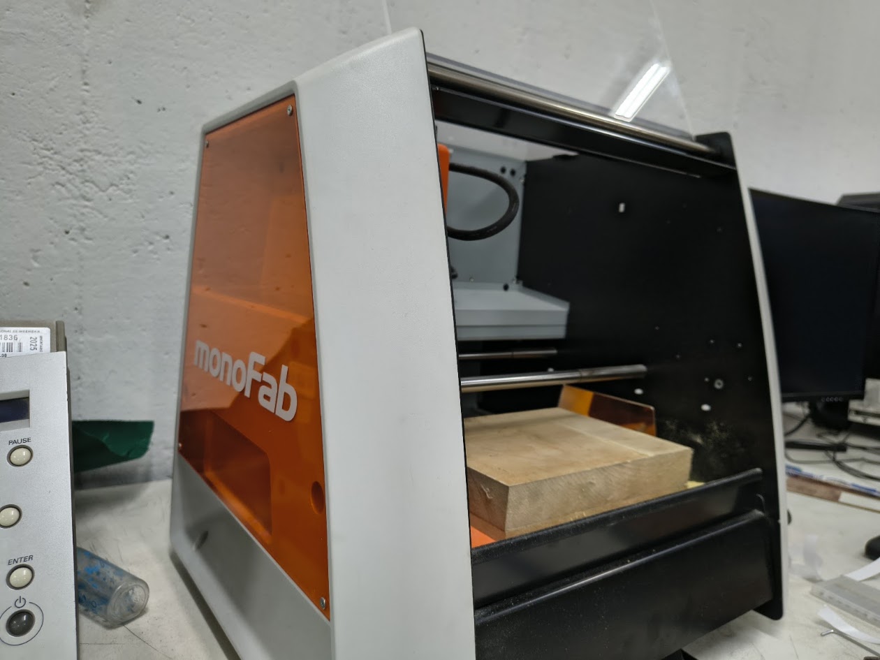
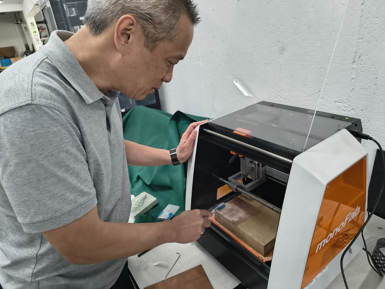
Milling: Roland MonoFab SRM-20 desktop CNC at Fab Lab UNI. MDF bed
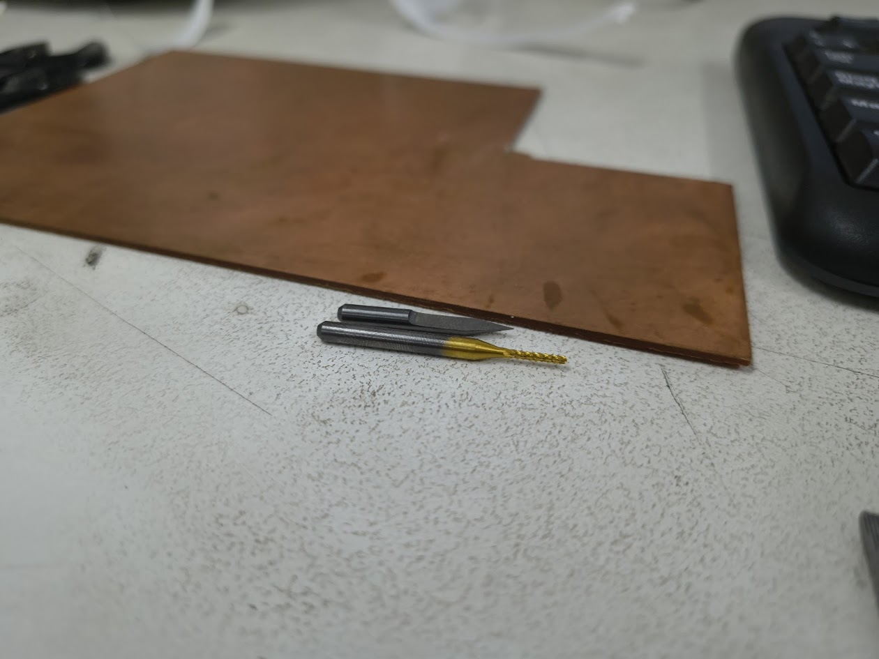
Milling: Copper-clad blank (35 µm Cu, 1.6 mm substrate). Cutting tools: a V-bit engraver (grey, flat tip) and a TiN-coated spiral drill bit (gold, for thruhole drilling)
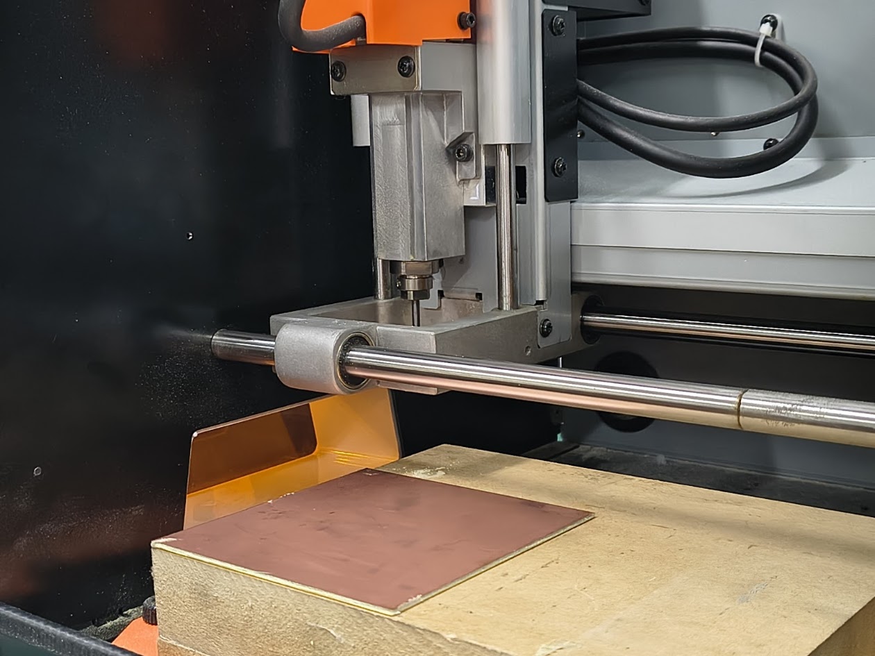
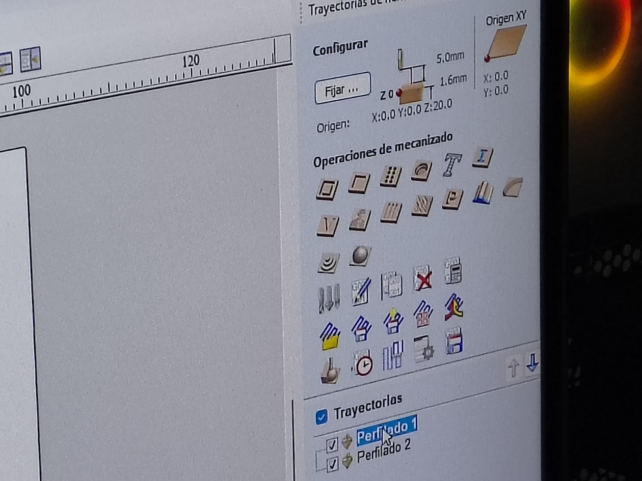
Milling: V-Bit 30° (0.1 mm tip) being inserted into the collet. Double-sided tape on the MDF layer. The spindle is positioned on XY origin
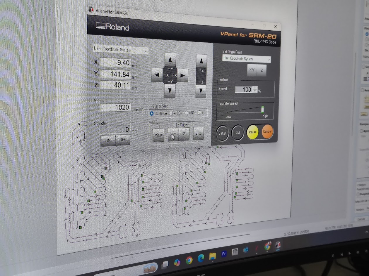
Milling: coordinates (X: -9.40, Y: 141.84, Z: 40.11 mm), spindle speed control, and the toolpath. Speed set to 100%
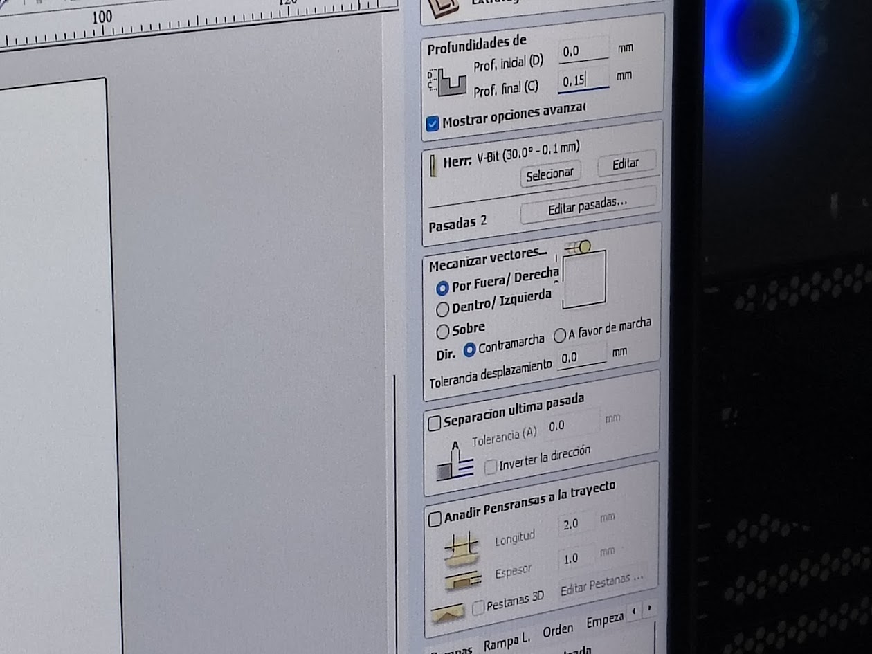
Milling: Initial 0.0 mm, Depth 0.15 mm, Tool V-Bit 30°–0.1 mm, passes 2
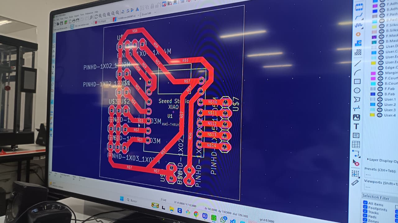
Milling: toolpaths, trace isolation, board outline cut
Milling: Aspire 2D view. CNC software
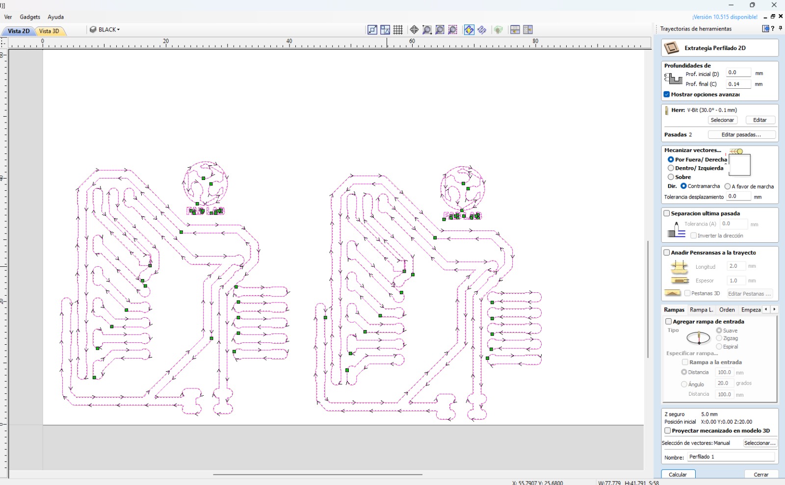
Milling: PCB milled simulation
Milling at Fab Lab UNI
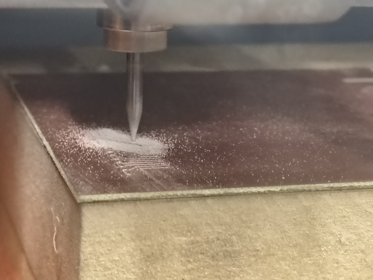
Milling in progress:copper traces are visible as fine white lines. The V-bit is cutting. Isolation confirm correct Z depth
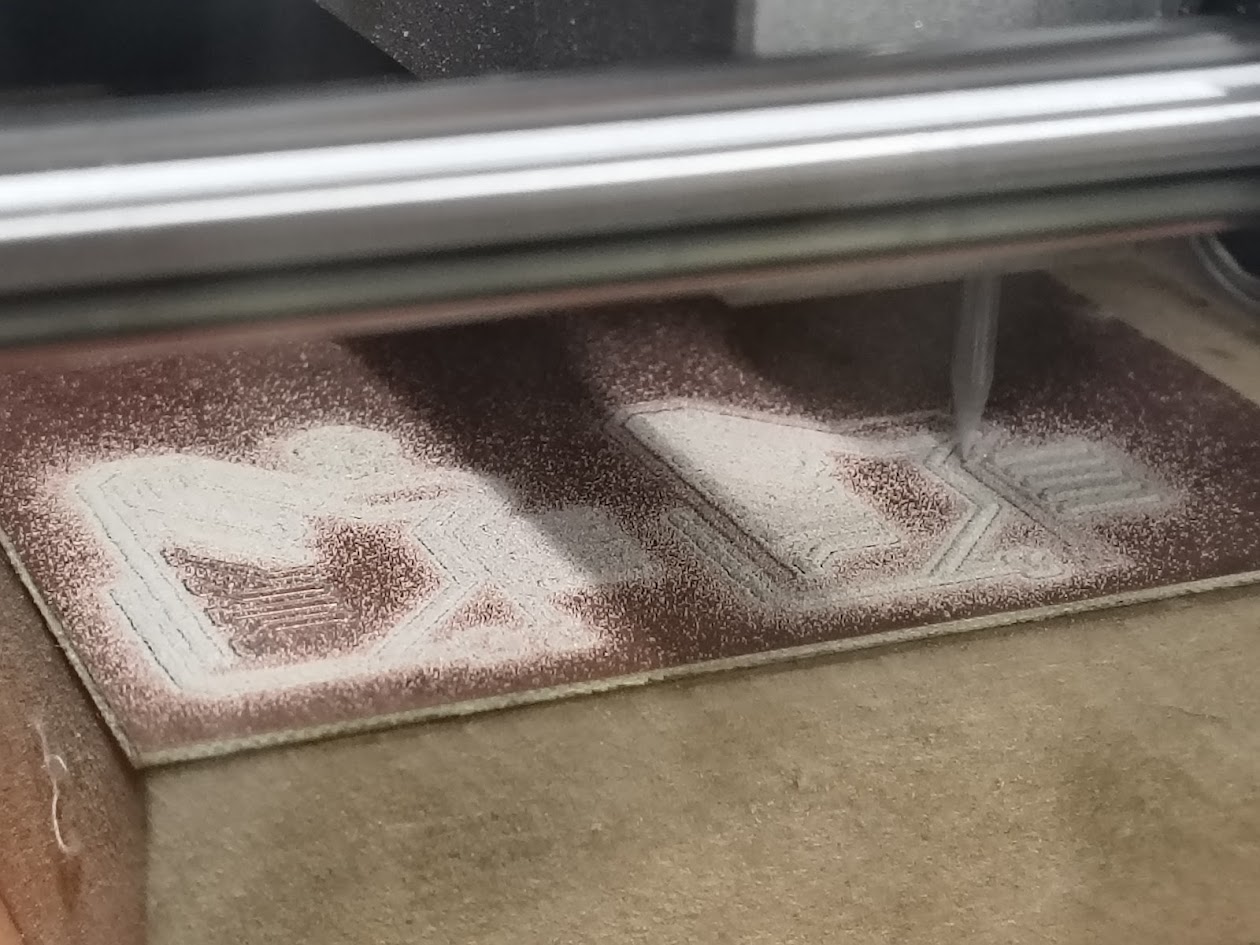
Milling in progress: board 1 completed and board 2 processing
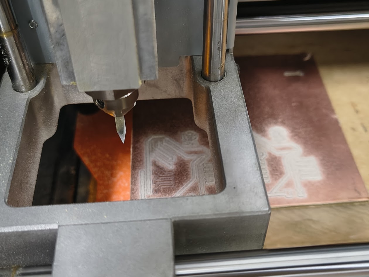
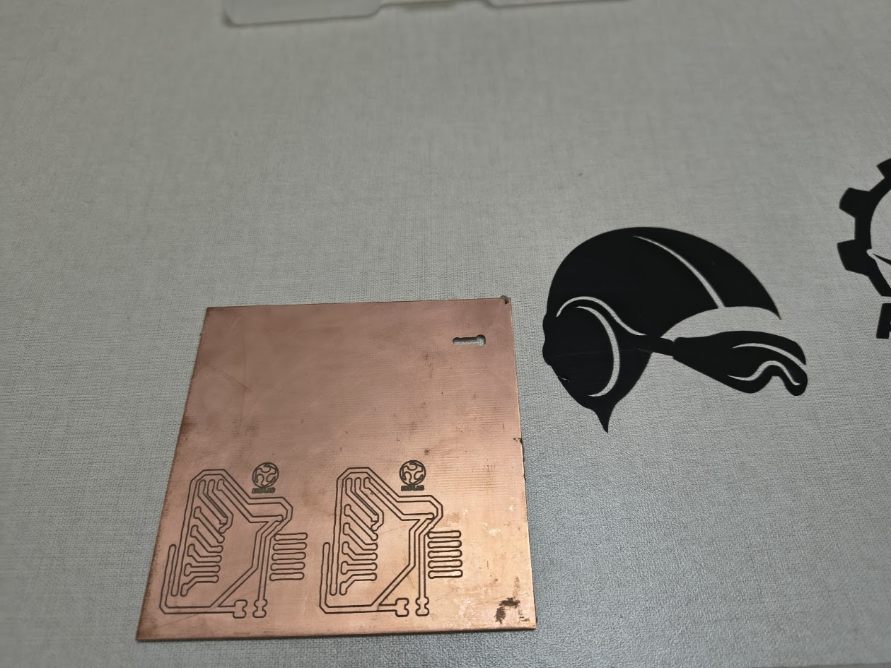
Milling completed
Milled completed: cleaning dust and reviewing the product. Aprox time 15 minutes
Milling completed:clean cooper surface
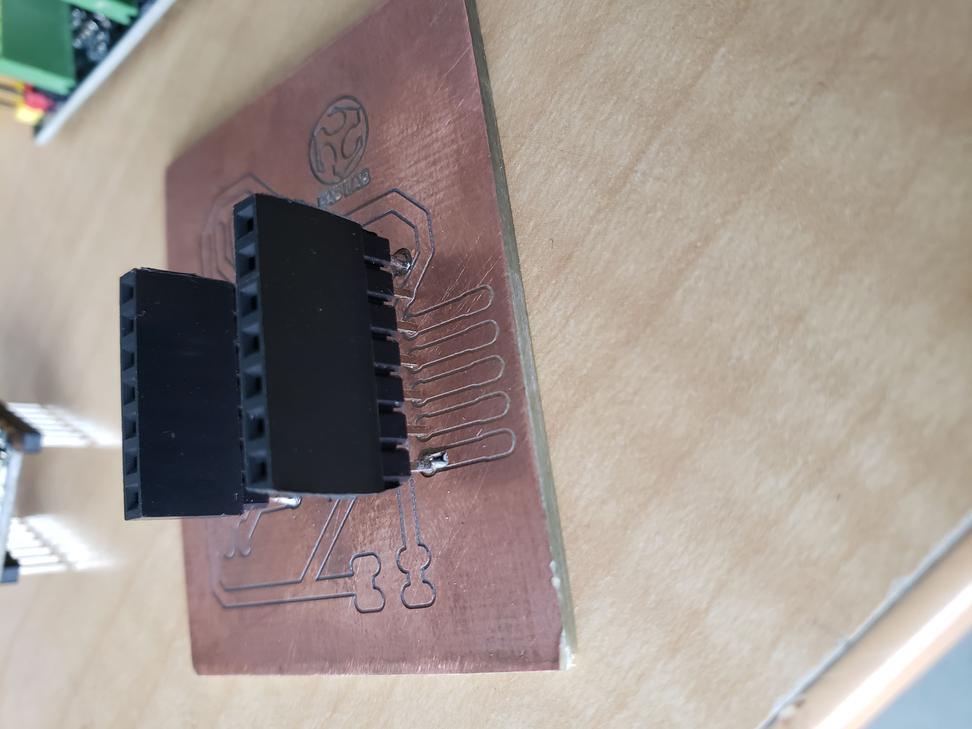
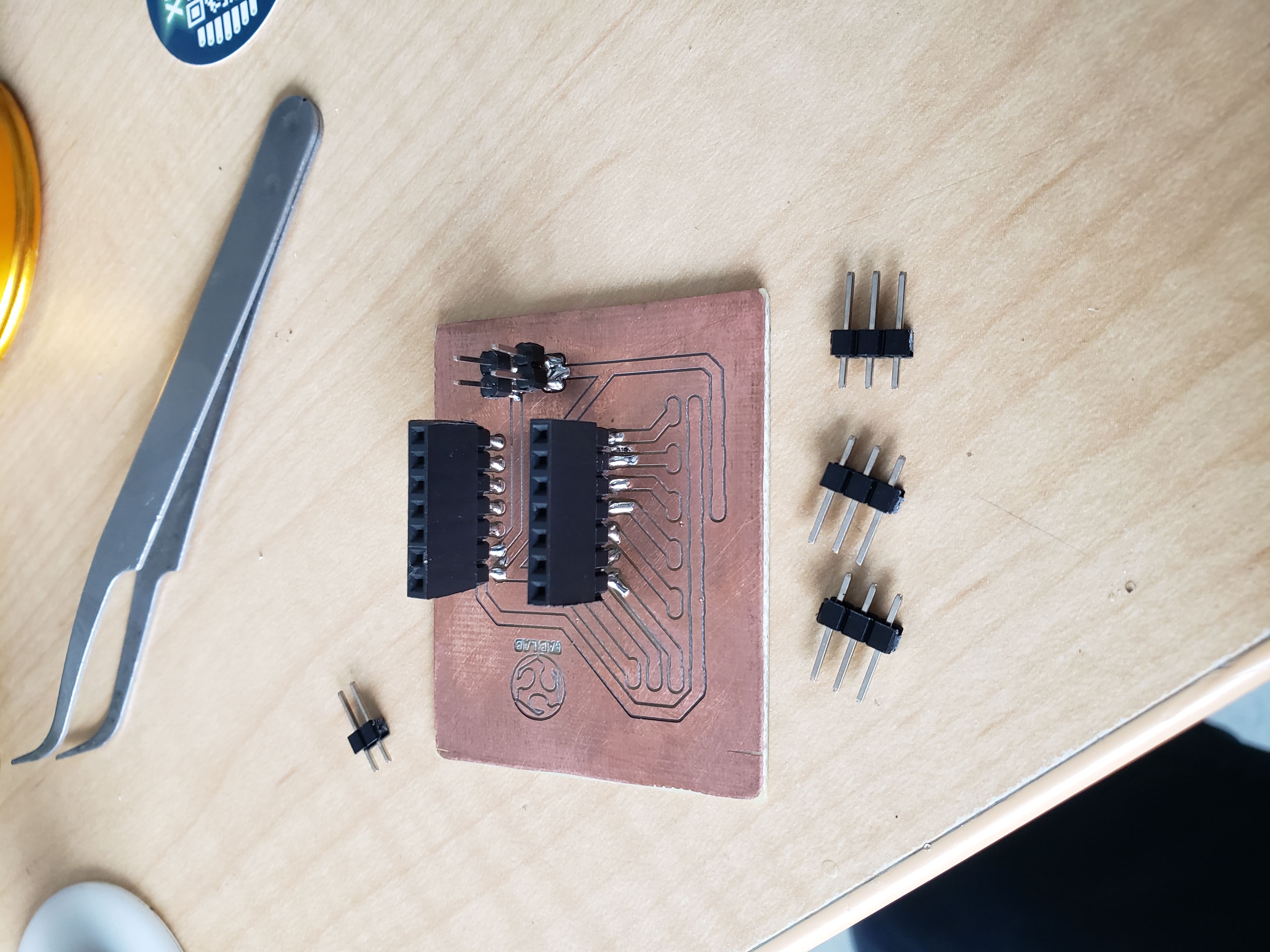
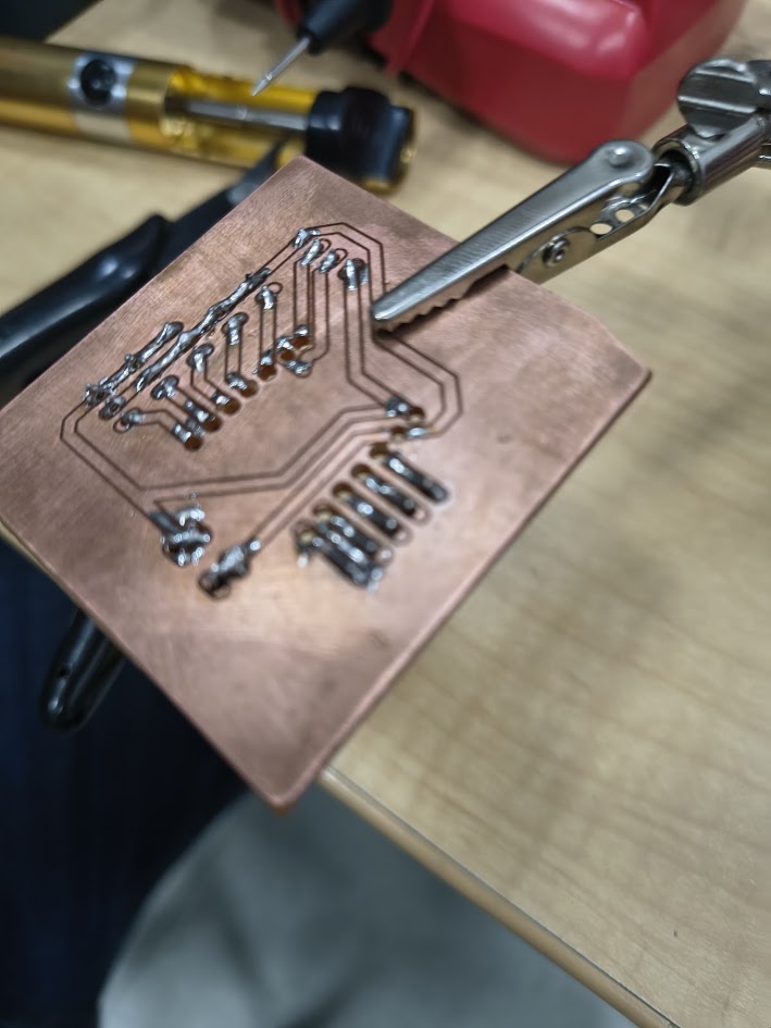
Soldering:02 female 7-pin socket headers
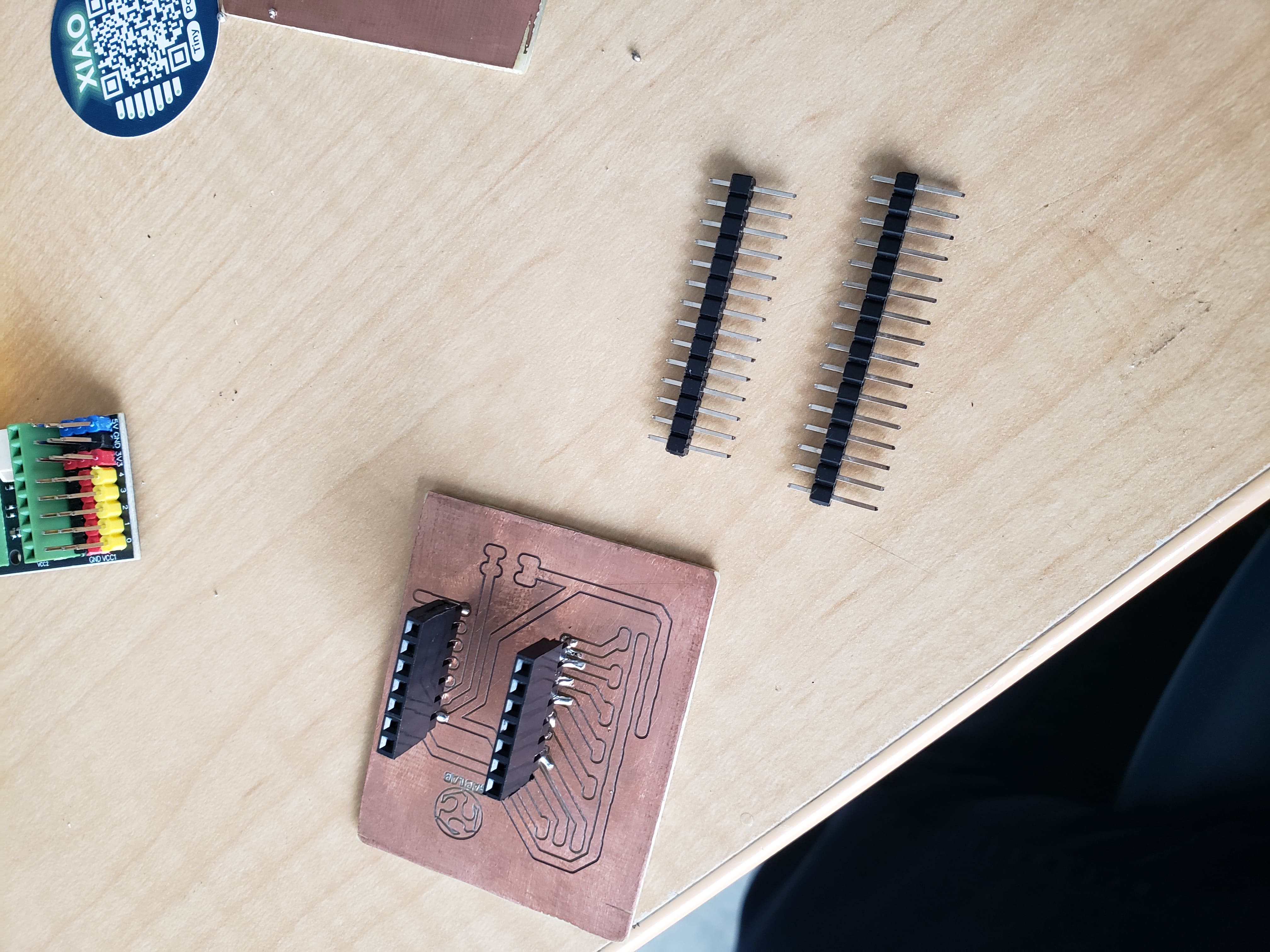
Soldering: PCB view and two 1x14 male strip headers
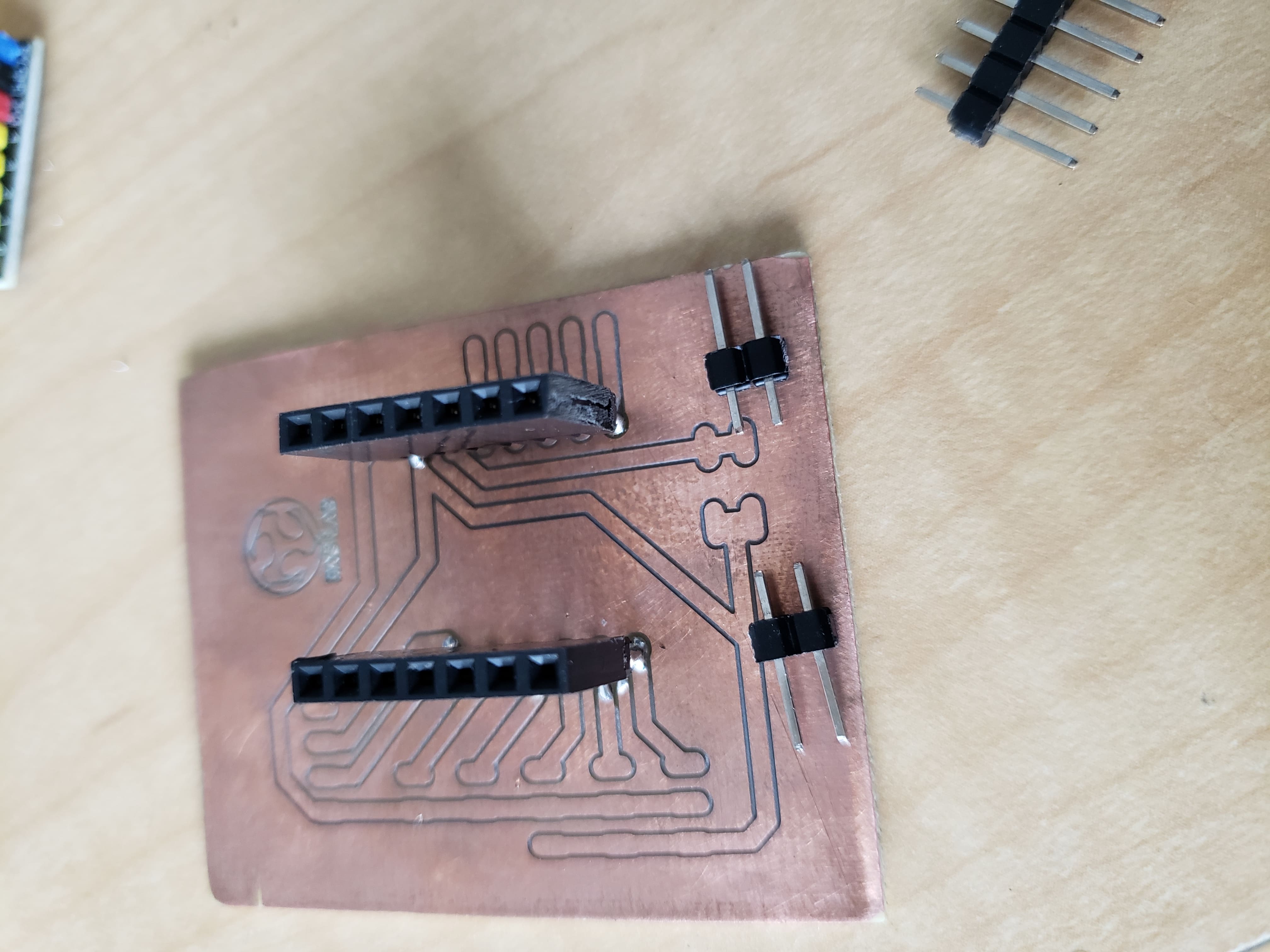
Soldering: 02 male 2-pin for VCC - 5v and GND connections
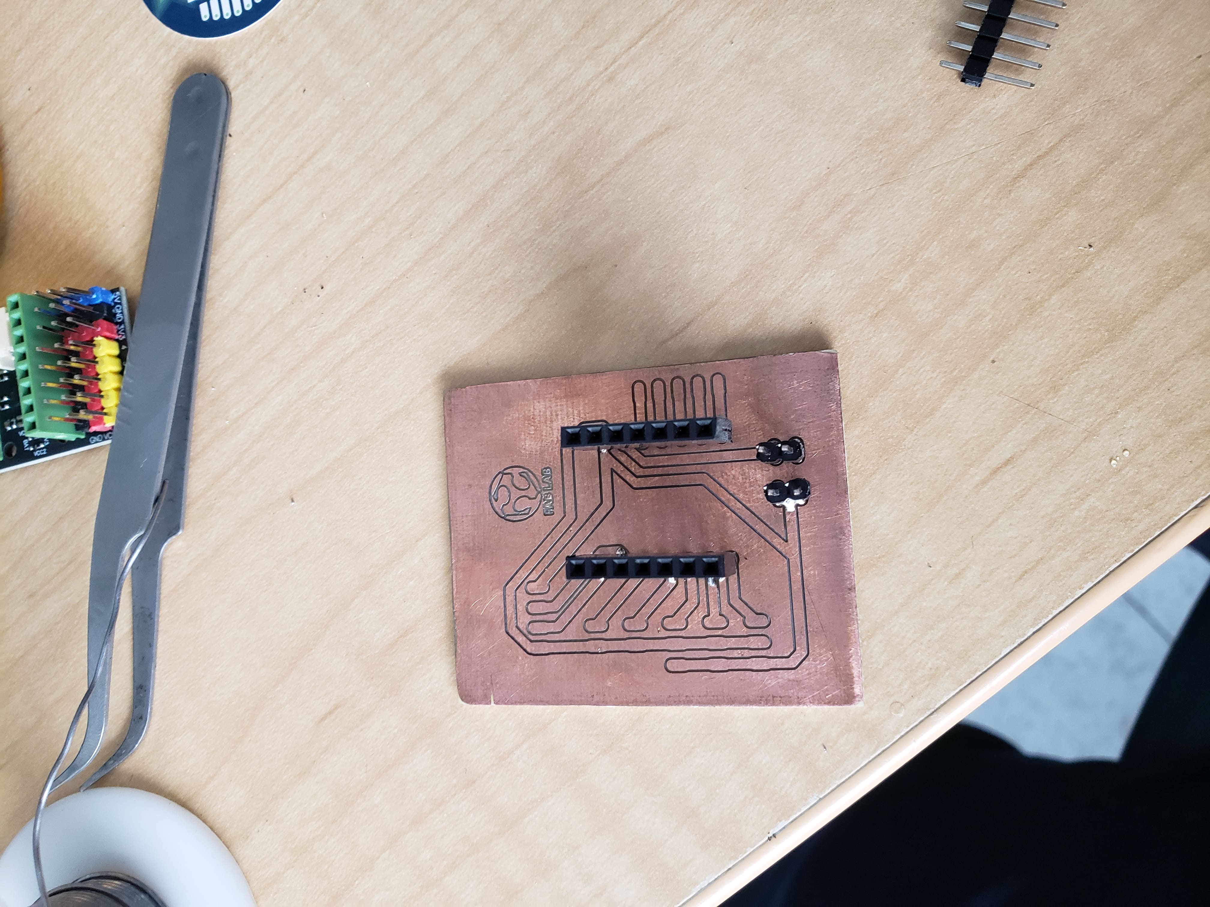
Soldering: Designed PCB production process - VCC 5v and GND
Soldering: D4, D5, D6 with GND and VCC
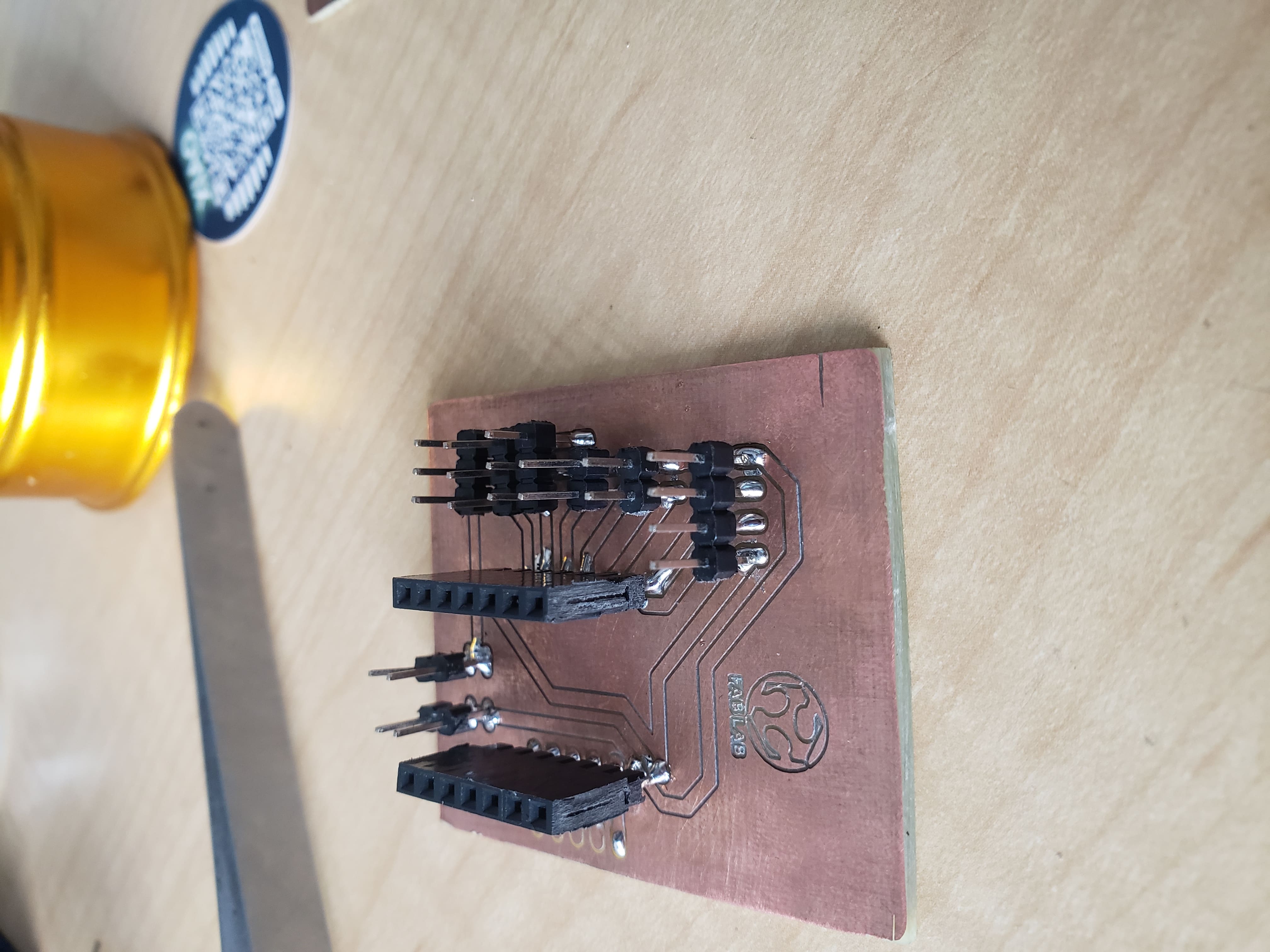
Soldering: VCC, D0, D1 and GND; D2, D3 and GND and D4, D5, D6, GND and VCC
Soldering: D7, D8, D9, D10 and 3v3

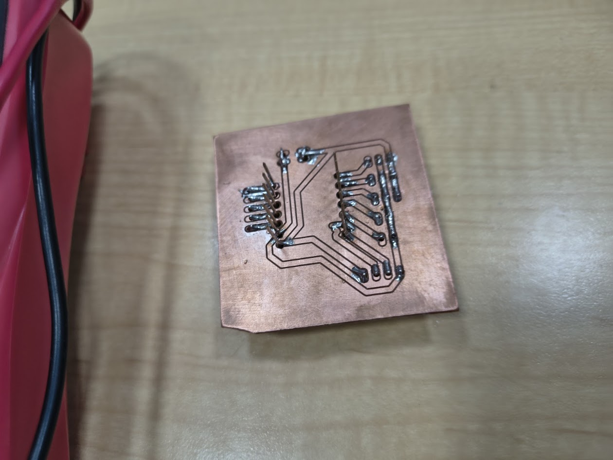
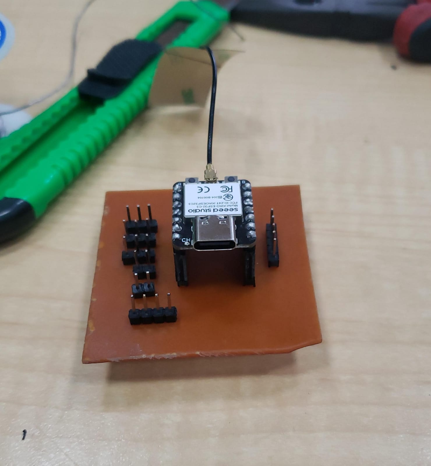
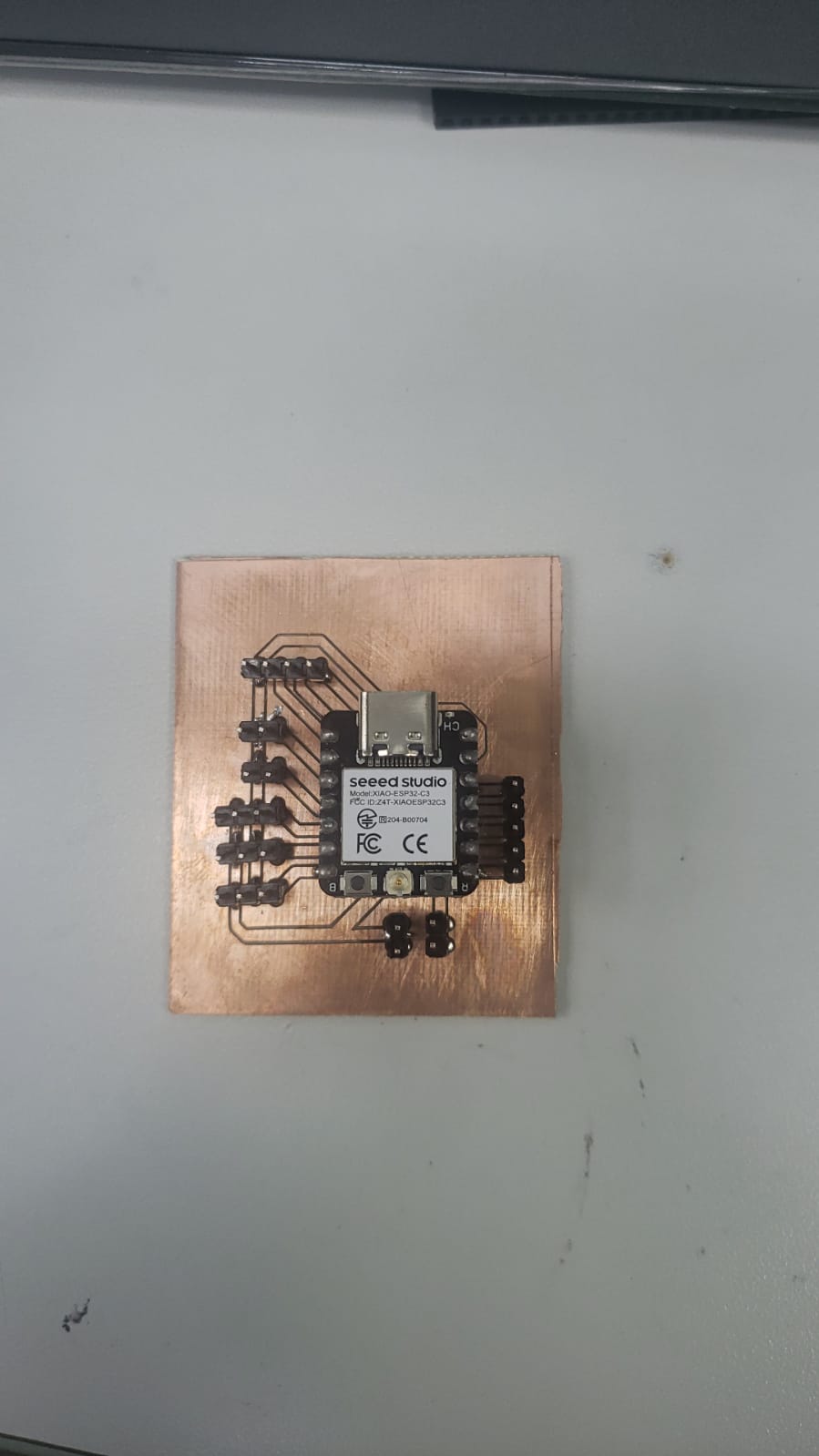
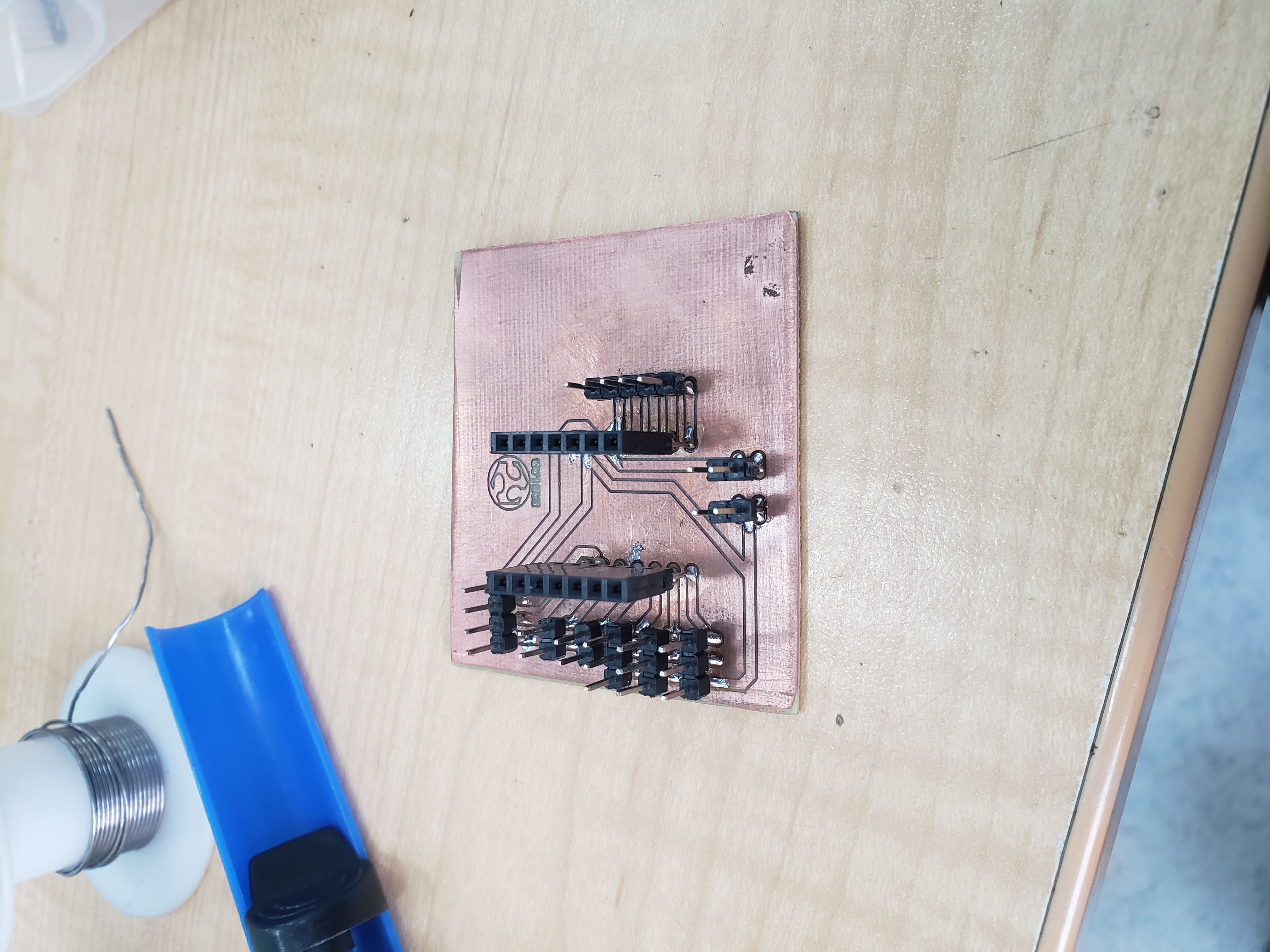
Final designed PCB with a Xiao ESP32 C3
The ERC (Electrical Rule Check) and DRC (Design Rule Check) processes are automated verification steps used during schematic capture and PCB layout to ensure your circuit is free of electrical faults and compliant with physical manufacturing limits
The ERC process evaluates the circuit schematic, logic, and electrical aspects. With the schematic PBC, I checked: Unconnected pins, short circuits, floating nets, incorrect power supply connections, and incompatible pins
The DRC process validates that your physical PCB layout, actual routing, component placement, and copper thicknesses, successful manufactured
With the routed PBC, I checked: trace widths, gaps between components, boundaries, and routes
DRC with the routed PBC
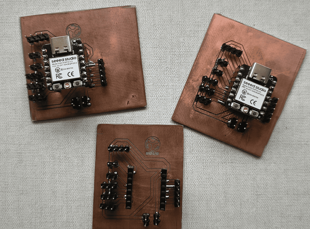
Three final PCB for the project
4) Final project advance
Running
Explore devices
Band for runners


5) Final results
- Linked to the group assignment page
- Documented how you made the toolpath
- Documented how you made (milled, stuffed, soldered) the board
- Documented that your board is functional
- Explained any problems and how you fixed them
- Uploaded your source code
- Included a 'hero shot' of your board
6) References files
We learn how to design, make and test a PCB. Files: