WEEK 8 ELECTRONICS PRODUCTION
INTRODUCTION
This week’s assignment consists of designing and manufacturing a Printed Circuit Board (PCB) using two different methods. The first one is to design it and send the files to a manufacturing company so they can deliver the finished PCB. The second one is to fabricate it locally at the Fab Lab using a dedicated milling machine.
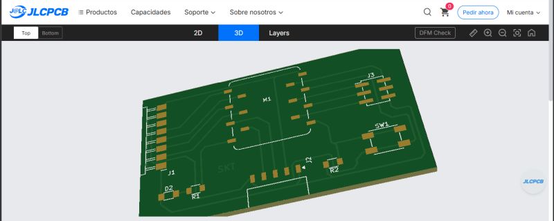
The first part, the design stage, was already completed, since we will use the board we created during Week 6, Electronics Design, using KiCad.
SCHEDULE
This week, due to family matters, I did not have much time available, so fitting the work in was another challenge for me.
- On Friday, from 9:00 p.m. to 12:00 p.m., I completed the tasks needed to prepare the “.rml” files required to mill the PCB on Saturday morning. At the same time, I also worked on the part of the assignment related to sending the Gerber files to a manufacturer so they could produce the board.
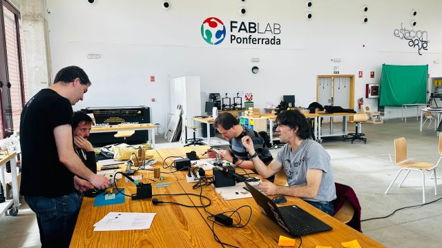
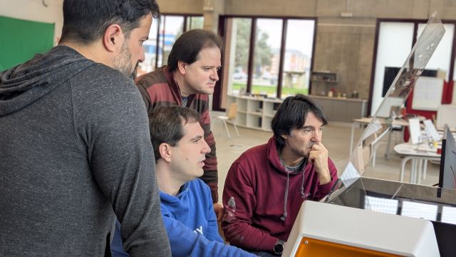
- On Saturday morning, we worked at the Fab Lab using the milling machine and soldering the components in order to finish the PCB.
- On Sunday, throughout the whole day, I completed the documentation work, including editing the texts, preparing the photos, and creating the HTML web page for the group assignment.
- On Monday, after the meeting with my instructors and classmates, I was able to finish the individual part of the assignment. On Tuesday, after work, I polished the final details.
As in other weeks, the work is divided into two parts
GROUP ASSIGNMENT
FabLab Leon work groupMILLING MACHINE
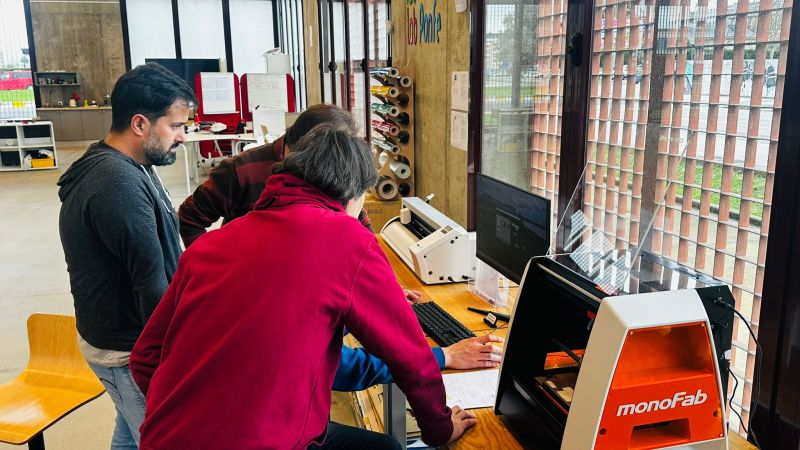
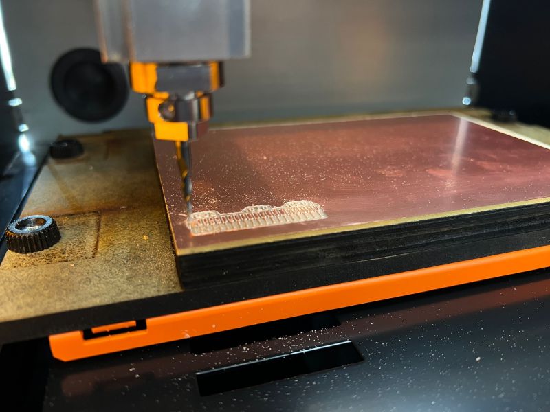
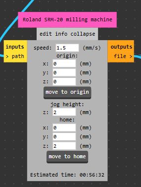
To manufacture the PCB at Fab Lab Ponferrada, we used a Roland MonoFab SRM-20 milling machine controlled through the VPanel for SRM-20 software.
The tool, meaning the milling bit we used, was a RO.25-15-D3.175-TiAIN. Its tip radius is 0.25 mm, but for the milling machine configuration we set it as having a 0.4 mm diameter, based on the previous experience of our instructors and the finish this bit usually provides.
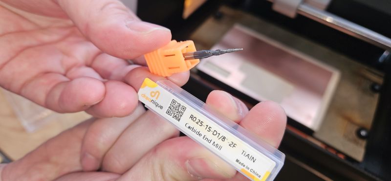
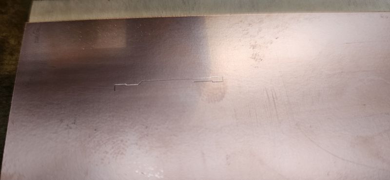
To carry out an initial test of the milling machine and check the resulting finish, we used the following test model:

ROLAND WORKFLOW
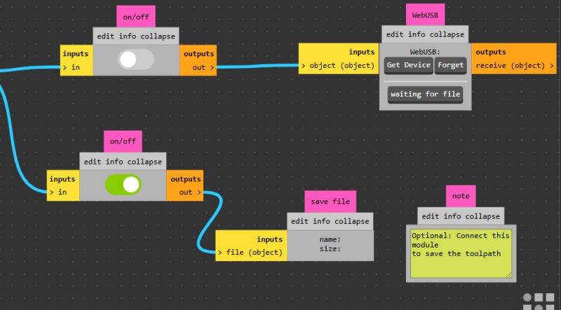
Below is the workflow we followed at the Fab Lab when using the milling machine. We start from the assumption that the trace files (files.rml) have already been generated beforehand. This part can be done on any computer, and I explain it later in the individual assignment.
VERY IMPORTANT: The milling machine must always be handled by only one person at a time, in order to prevent the spindle from starting because of one person’s command while another person is manipulating it.
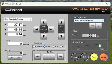
- We turn on the milling machine using the power button located on the upper part of the machine and launch the VPanel SRM-20 application on the computer.
- We verify the connection between the milling machine and the computer, and we check that the machine moves correctly by manually moving the head along the X, Y, and Z axes. Great care must be taken at this stage with the movement scale in order to prevent the spindle from crashing into anything.
- We prepare the work material by fixing the copper board onto the sacrificial layer of the bed using double-sided tape.
- We place the milling bit into the spindle and secure it with the corresponding set screw. At this point, we have two types of bits to choose from:
- 0.4 mm for milling, which is the one we selected in this case.
- 0.8 mm for cutting.
- We adjust the X and Y origin position and save it by pressing Set Origin Point XY.
- We carefully lower the bit as close as possible to the material without actually touching it.
- We manually adjust the height of the bit by loosening the spindle set screw and lowering the bit by hand until it touches the material, then tightening the screw again.
- We save the Z origin position by pressing Set Origin Z.
- We raise the Z axis by 3 mm by pressing the manual Z movement button three times at x100 scale.
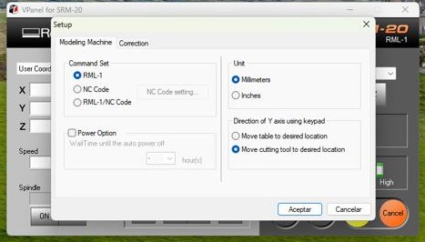
- Once the origin is set on all axes, we proceed to configure the software Setup.
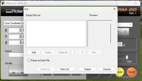
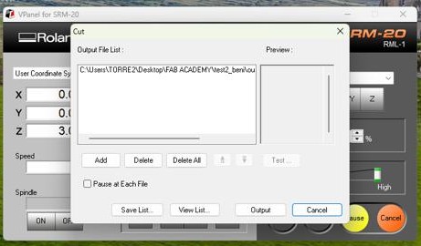
- We press CUT. Important: the milling machine cover must be closed, otherwise this step cannot be performed.
- We delete any files that may already be loaded and import our traces.rml file.
- We press Output, and the milling machine starts running.
- At this point, it is recommended to reduce the spindle speed to 20% to check that everything is going well, and if everything looks correct, increase it again to 100%.
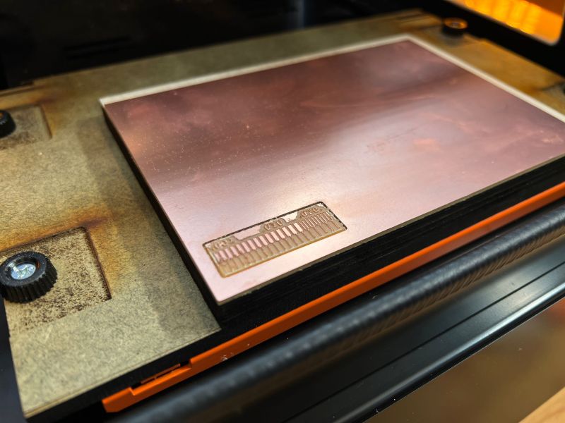
- Once the milling machine has finished and stopped, we can press View so that the spindle moves away and the bed comes out toward us, after opening the machine cover. Using a vacuum cleaner, we remove the copper dust deposited on top of the PCB and inspect whether the result is correct.
- To make the outer cut, we raise the spindle and change the bit to the 0.8 mm one, repeating the Z-axis adjustment in the same way as before, but being very careful not to change the XY origin.
- We raise the Z axis by 3 mm again, close the cover, and return to the CUT menu.
- We delete the previous file and import the cutting (file.rml) file.
- We press Output, and the milling machine starts again. In the same way, we can reduce the spindle speed to 50% at first to make sure everything is working correctly, and then bring it back to 100%.
- Once finished, we press View again and, after vacuuming the area, we can remove our PCB.
There are three movement scales: step x1, x10, and x100, where each click moves the head by that number of steps, with 100 steps being equal to 1 mm. There is also a continuous mode, in which the head moves as long as the button is pressed. This option is not recommended for the Z axis, since it moves too quickly.
PROBLEMS
In practice, and despite having followed all the steps, our first PCB was a complete disaster.
As we have seen, setting the Z-axis origin correctly is essential, because if the bit does not go low enough, it will not properly touch the material and therefore it will not mill it. But if it goes too low, it will remove too much material and may even break the traces.
Although the Z-axis origin had been set correctly, there was another issue: the bed was not properly leveled. Since the bed was uneven, the actual Z position changed as the bit moved along the XY axes, which meant that in some areas the bit dug too deeply into the material, while in others it barely touched it. This made the final result completely unusable. Only after the bed was repaired did the milling machine work correctly again.
SENDING THE BOARD TO A FACTORY
Another way to obtain a PCB is to send it to an external manufacturer. To do this, we first need to have a design, made for example in KiCad:
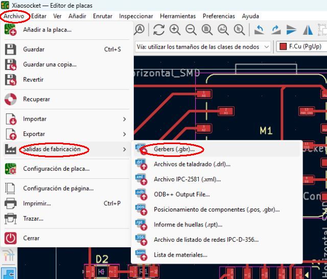
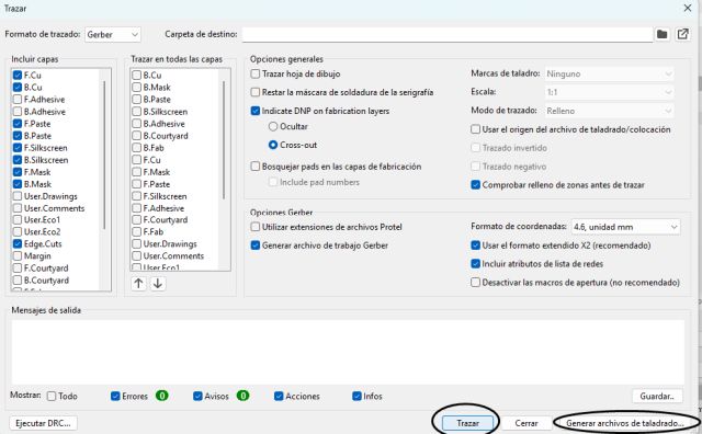
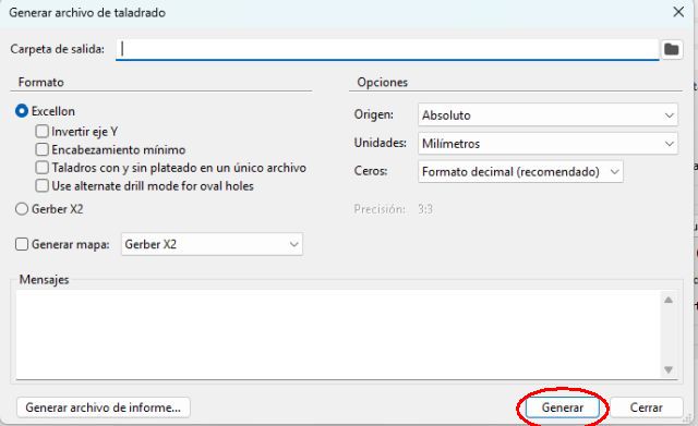
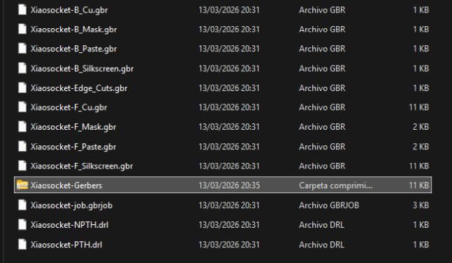
From KiCad, we use the option “Fabrication Outputs” → “Gerbers (.gbr)”, which generates a series of files that can be compressed into a single .zip file.
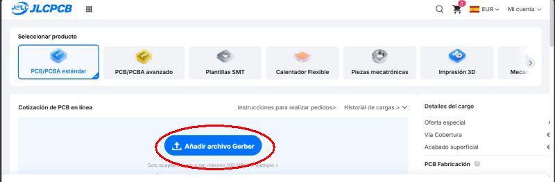
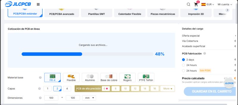
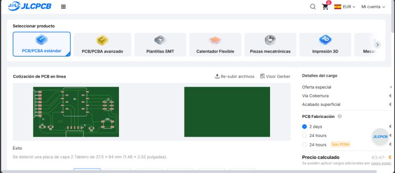
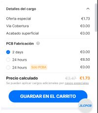
Once we have that file, we can go to a PCB manufacturer’s website. In this example, we chose JLCPCB. On their website, after creating an account and logging in, we go to the “Order PCB” option, choose the type of board we want, and upload the gerber.zip file that we created in KiCad. In this way, the manufacturer receives all the information needed to produce the board, and the only things left to do are pay and wait for it to arrive.


There is also the option of ordering not only the PCB and soldering the components ourselves afterward, but also, by sending the Gerber, BOM, and CPL files, ordering the board with all components already soldered.
INDIVIDUAL ASSIGNMENT
Design and configuration
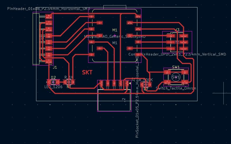
In the individual assignment, I am asked to design and fabricate an electronic development board with a microcontroller and verify that it works properly.
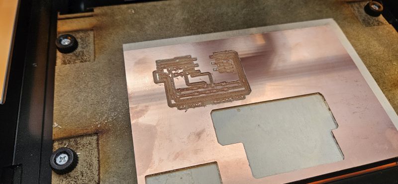
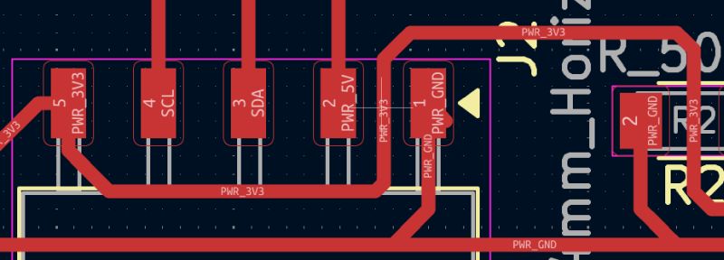
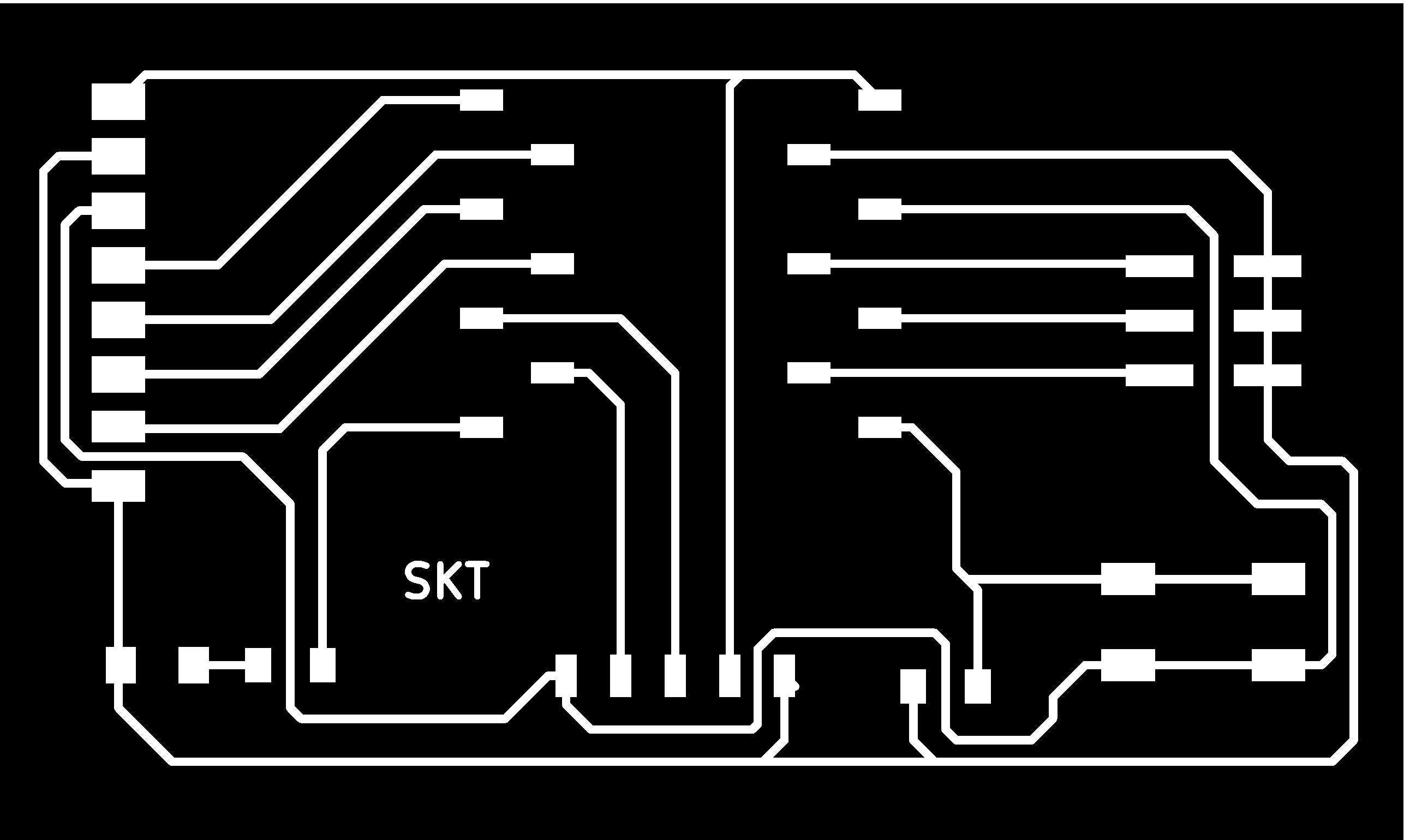
For this assignment, I already had the board designed from the previous week. However, to fabricate it using the milling machine, I had a small problem.
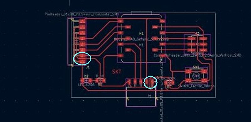
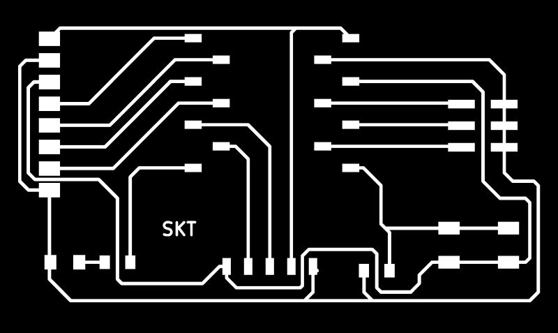
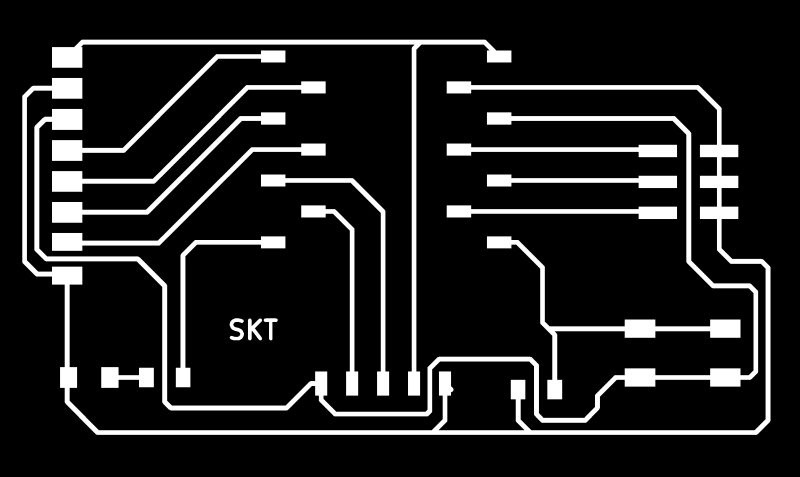
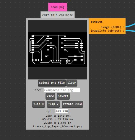
The two highlighted traces pass too close to the connector pads, which means that the milling bit will not be able to pass through that gap and therefore will not mill that trace properly. The lower one can be fixed directly in KiCad, but the one on the left will require a workaround later.
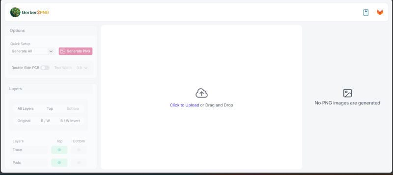
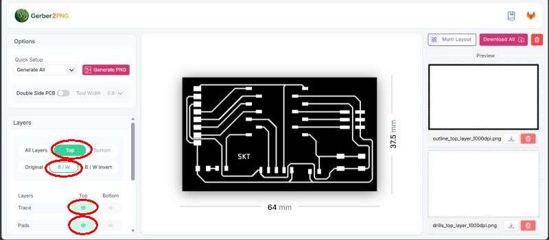
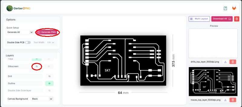
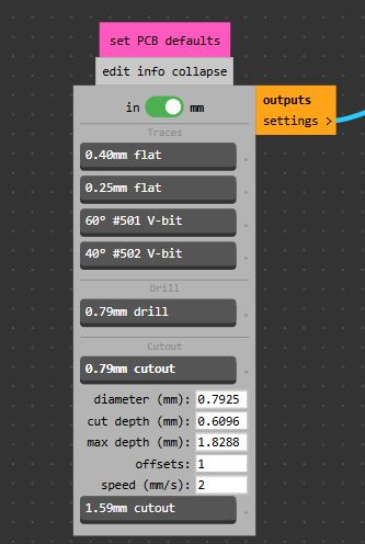
As before, I obtained the trace files and drill files (if any) directly from KiCad. Then I processed the compressed .zip file through the Gerber 2 PNG application in order to obtain three .png files: one for the traces, one for the drills, and one for the outline cut. These are the files I later used to configure the milling process in the MODS application.
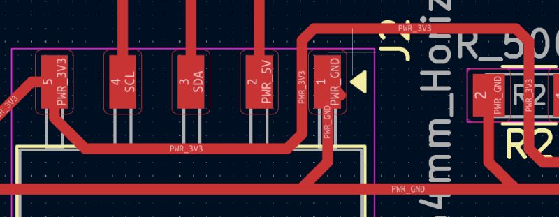
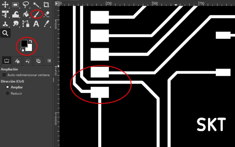
But before that, I had to fix the trace that did not fit between the pads on the left side. The trick to solve this was to edit the .png file in GIMP and make the pads thinner in order to leave enough room for the trace.
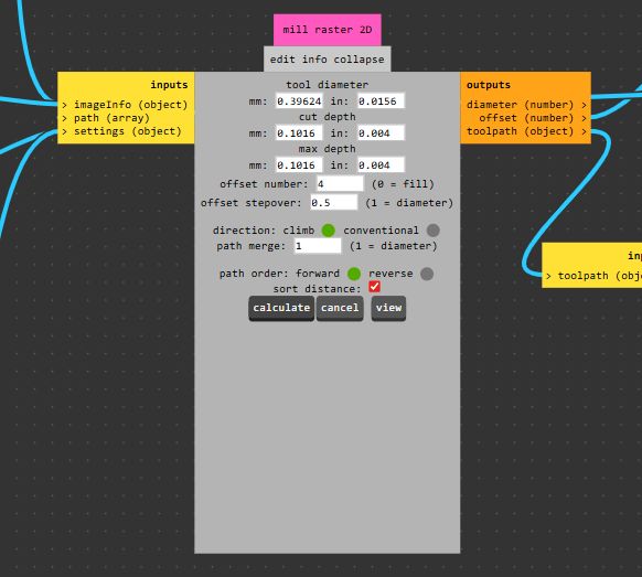
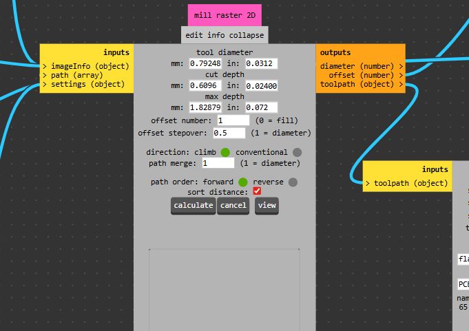
Once I had the .png files, I went to the MODS application, where I configured the milling process.
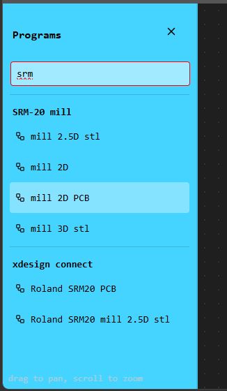
Once inside MODS, I selected the milling machine I was going to use, in this case SRM-20 mill 2D PCB, and I obtained the following workflow:
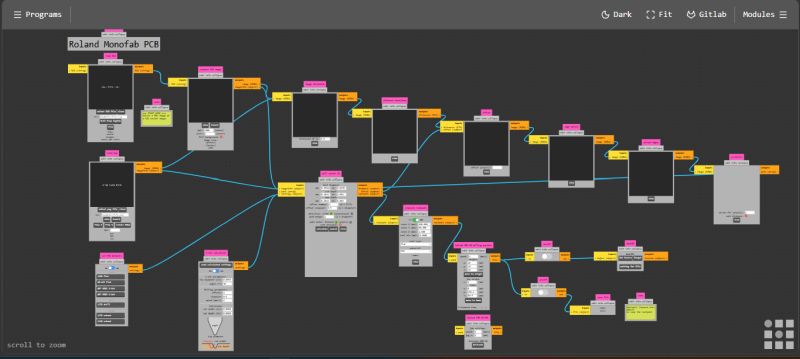
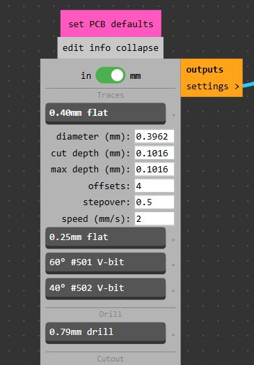
In this diagram, I selected the necessary settings for the milling, drilling, and cutting of the PCB.
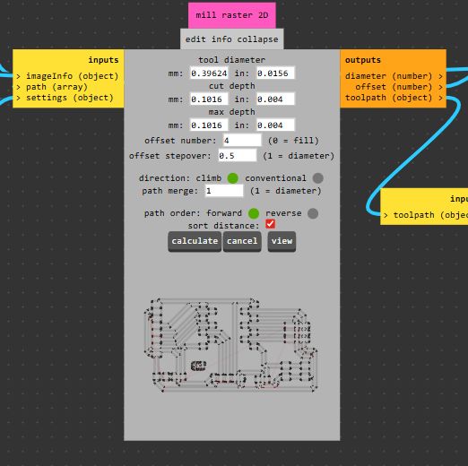
MILLING
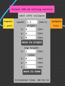
CUTTING
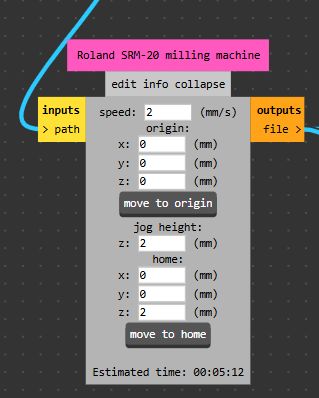
Once all the parameters were configured, I pressed Calculate and obtained the .rml files that I finally used to run the milling machine, following the workflow described in the Group assignment section.
SOLDERING
Once the boards were milled, it was time to solder the components one by one. In my case, these were:
- A Raspberry Pi RP2040 microcontroller
- Two sockets and pin headers to mount and remove the controller
- A push button
- Two resistors, one 1kΩ and one 10kΩ
- One LED
- Two horizontal female connectors
- One vertical male connector
The soldering process is simple, but tedious. It is a tin soldering process in which, after cleaning the surfaces to be soldered and applying a small amount of flux to prepare them, we heat the two parts to be joined with the soldering iron, and once they are hot enough, we apply solder (pewter) seeing how it flows around and joins both surfaces. Once this happens, we remove the soldering iron and allow everything to cool down, so the solder solidifies and leaves both parts joined together.
I have to say that this process is not unfamiliar to me, because I sometimes also have to solder with tin at work. However, the difference is that I had never soldered such small components before. The smallest things I had soldered previously were electrical wires connected to different electrical components in medium- and low-voltage panels. Soldering while holding the component with tweezers and using a magnifying glass was quite challenging for me.
FUNCTIONAL TEST
Once I had the finished PCB in my hands, it was time to test whether it worked. First, using the multimeter in continuity mode, I checked trace by trace that there was continuity where there should be. At the same time, I also verified that there was no continuity between different traces, meaning that no unwanted bridges had been created during soldering, which would not have been surprising considering how close everything was.
Once the “cold test” was completed, the moment of truth arrived: the RP2040 was connected to a power supply through its USB-C port and... it worked!!
The next step was to create an Arduino program, upload it to the controller, and check whether the rest of the board was also working. In my case, since I still do not have enough experience to write the code entirely by myself, I asked ChatGPT to generate one for me. The prompt I used was:
“I have a PCB with a Xiao RP2040 controller. Please give me an Arduino code to verify its operation. I am sending you the electrical schematic of the board.”
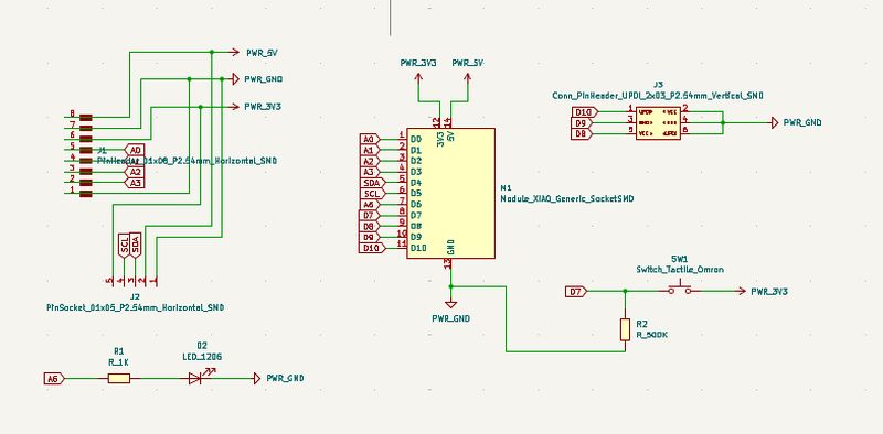
ChatGPT recognized the components in the schematic and offered me several options, from which I chose the following one:
Arduino code
          const int ledPin = D6;
const int buttonPin = D7;

bool ledState = false;
bool lastButtonState = LOW;

void setup() {
  pinMode(ledPin, OUTPUT);
  pinMode(buttonPin, INPUT);

  digitalWrite(ledPin, LOW);

  Serial.begin(115200);
  delay(1000);
  Serial.println("Inicio del test");
  Serial.println("Pulsa el boton para cambiar el estado del LED");
}

void loop() {
  bool currentButtonState = digitalRead(buttonPin);

  // Detecta la pulsacion
  if (currentButtonState == HIGH && lastButtonState == LOW) {
    ledState = !ledState;
    digitalWrite(ledPin, ledState ? HIGH : LOW);

    Serial.print("Boton pulsado -> LED ");
    if (ledState) {
      Serial.println("ENCENDIDO");
    } else {
      Serial.println("APAGADO");
    }

    delay(200); // debounce sencillo
  }

  lastButtonState = currentButtonState;
}
Once the program was compiled, I could see that the LED turned on and off each time I pressed the button.
Mission accomplished!!
CONCLUSION
For me, this assignment had two clearly differentiated parts. Leaving aside the software aspect, the practical or hands-on work consisted of two main processes: milling and soldering.
Regarding the milling process, my previous experience with milling machines helped me in the same way it did during last week’s assignment. In the end, both machines are CNC mills, but with different sizes and levels of precision. With the milling machine used this week, precision is the most critical factor. Milling such small traces requires very delicate movements and, as we were able to observe, any small error—whether in the bed leveling or in the zero adjustments, especially on the Z axis—can significantly affect the final result. These small inaccuracies can easily make the difference between a functional PCB and an unusable one.
As for soldering, as I mentioned before, I occasionally solder with tin in my job. However, I usually work with a flat-tip soldering iron on cables of 1.5 mm or larger, connecting them to potentiometers, capacitors, and other components that are significantly bigger, since these connections are typically between two and five millimeters. In addition, I also solder copper pipes of 10, 15, 18 millimeters or more using a torch. Because of this, soldering such small components on a PCB felt unusual at first, but at the same time it was a very rewarding experience. Nevertheless, I still need more practice to achieve cleaner and more elegant solder joints.