6. Electronics Design
- Group assignment
- Use the test equipment in your lab to observe the operation of a microcontroller circuit board (as a minimum, you should demonstrate the use of a logic analyzer)
- Document your work on the group work page and reflect what you learned on your individual page
- Individual assignment
- Use an EDA tool to design a development board that uses parts from the inventory to interact and communicate with an embedded microcontroller
Group Assignment
For the group assignment we explored the test equipment in the lab and used them to observe and analyse a working microcontroller circuit.
Multimeter (ZOYI ZT301) used for checking continuity across traces, measuring voltage on the 3.3V and 5V rails, and verifying resistor values.
Oscilloscope (OWON TAO3104A) used a XIAO RP2040 as a function generator to output different waveforms via PWM and observed them live. Since the RP2040 outputs digital PWM, waveforms like sine and triangle are approximations, zoom out on time/div to see the full envelope.
Logic Analyser (Saleae Logic 8) captured and decoded real communication protocols from the RP2040. UART decoded "hello world!" at 9600 baud, and I²C captured communication to an SSD1306 OLED display.
Bench Power Supply provides clean regulated DC power for testing. Set voltage and current limit before powering up.
Full group docs: https://fabacademy.org/2026/labs/kochi/group_assignmetns/week06/
Individual Assignment
Using Wokwi Extension in VSCode
To set up the .json config file, rename it to .txt, paste in the code from the online Wokwi simulator, then rename it back to .json.
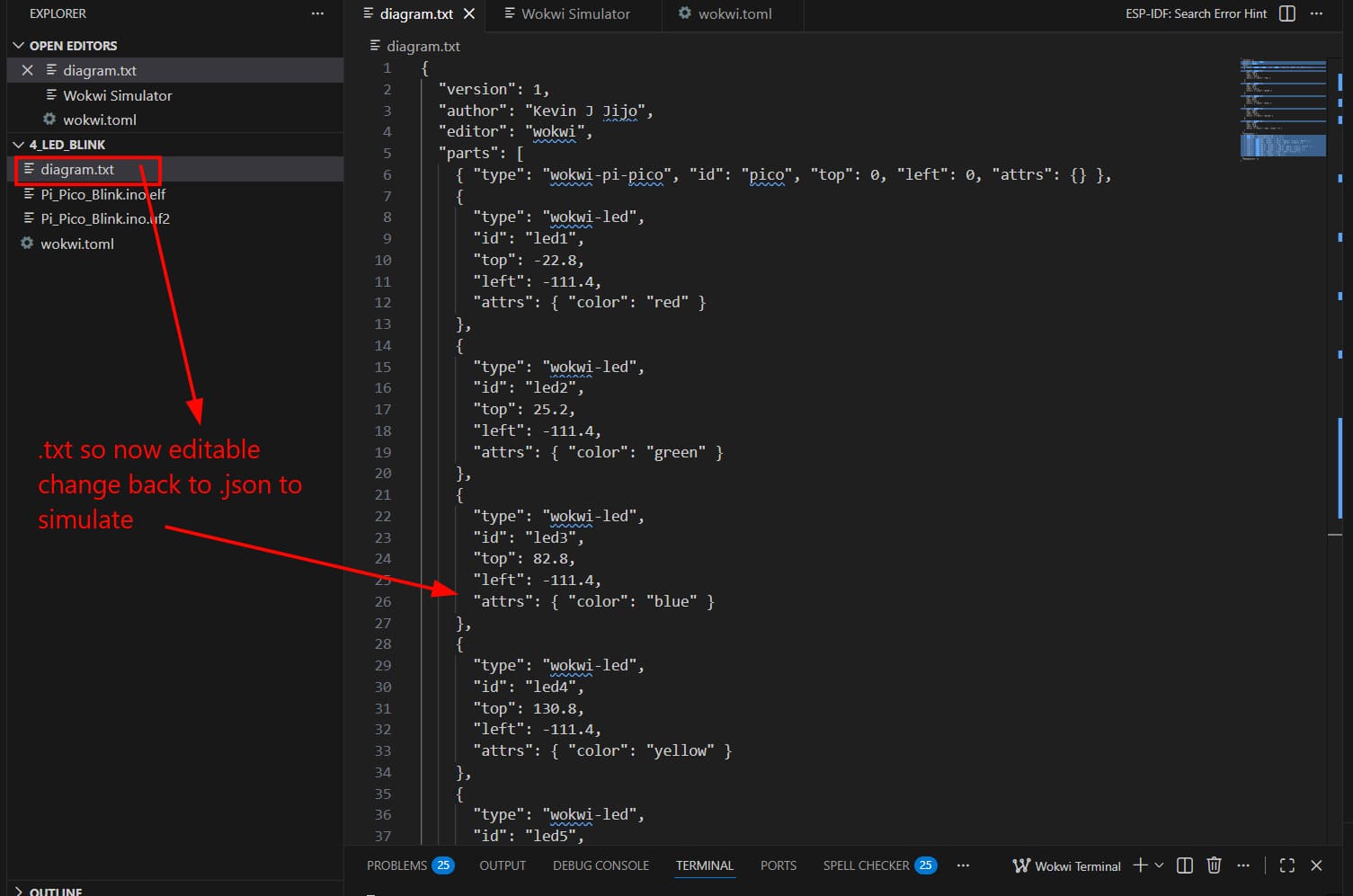
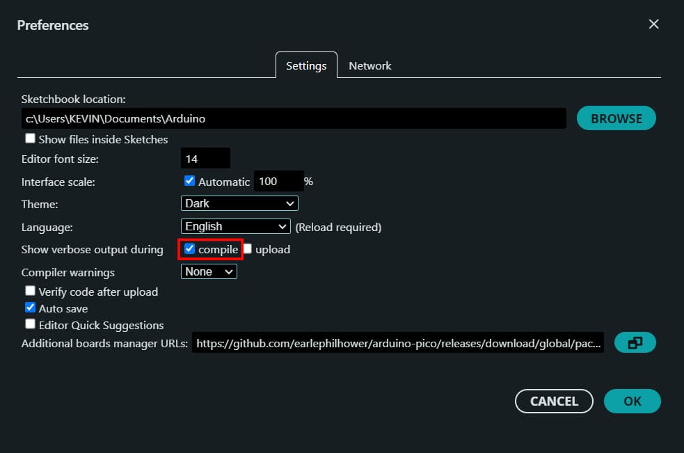
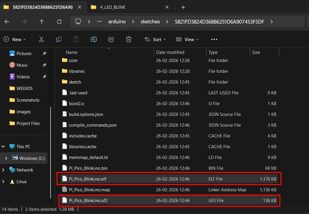
In Arduino IDE, go to File → Preferences and enable "Show verbose output during compile". Select the correct board and compile. Once done, the output terminal will show the path to your build directory — navigate there to find the .uf2 and .elf build files.
The output terminal displays the location of the build files. You can either point the .toml directly to that path, or just copy both files into your Wokwi project root folder.
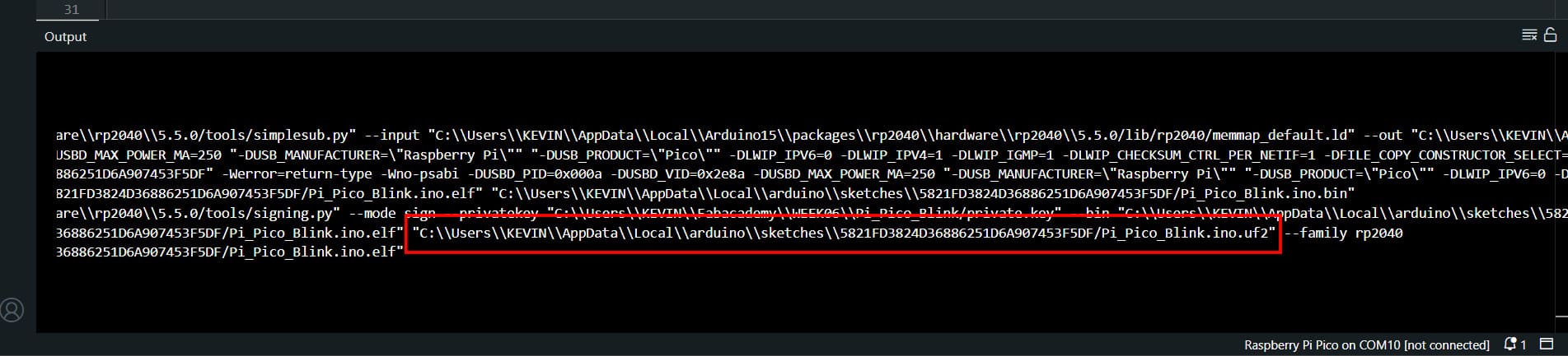
These are the two build files found at the compiled output path.
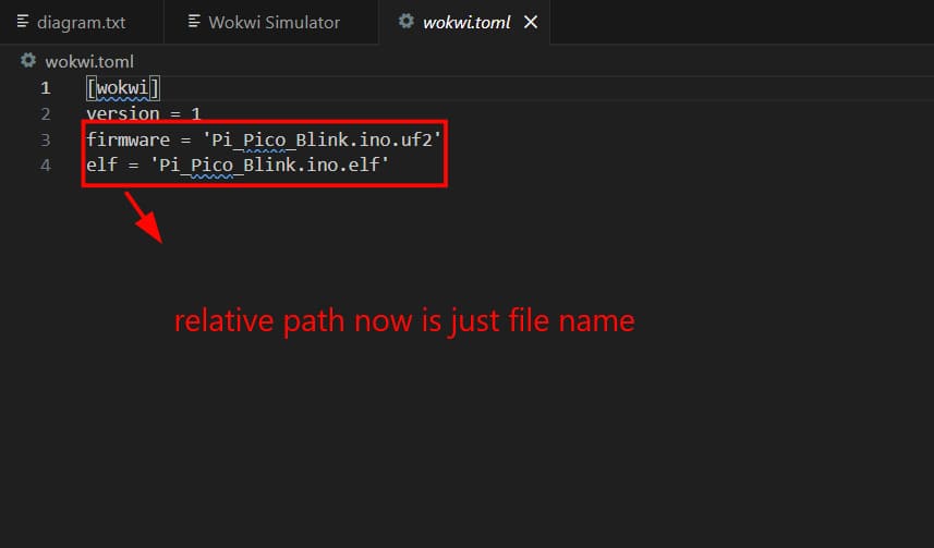
If you copy both files into the Wokwi root folder, the relative path in your .toml is just the filename itself.
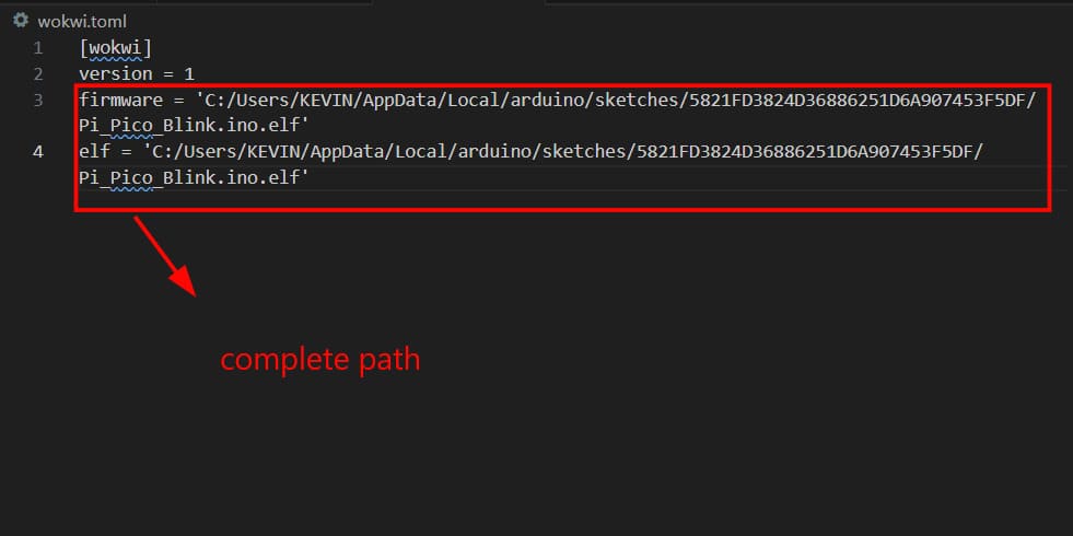
Alternatively, you can skip copying and just link the full absolute path to both files directly in the .toml.
ELF (Executable and Linkable Format) is the standard binary file format on Linux/Unix systems. It acts as a container for machine code and metadata, letting the OS load, link, and execute programs. The three formats compared:
- BIN — a raw byte-for-byte image of what goes into target memory. No gaps, no extras.
- HEX — a text representation of the binary with addresses and checksums, so it can be sparse.
- ELF — the full build output, containing the code plus symbol and debug info. BIN and HEX are both generated from the ELF.
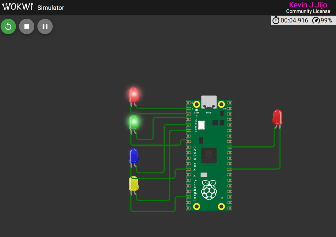
With that set up, we can now simulate!
Electronics Basics
Power = V × I
For example, my laptop charger runs at 170W — input is 220V at 0.7A, and the output is 20V at 8.5A, which is what the laptop actually needs to run.
SMD Resistor — Surface Mount Device. Sits flat on the PCB surface rather than having legs that go through holes.
The Fablab Kerala inventory of components and materials can be found at: https://inventory.fablabkerala.in/
Image Credits: Source
Transistor — three terminals: Base, Emitter, Collector.
MOSFET — three terminals: Gate, Source, Drain. The insulating layer inside is formed from SiO₂ (silicon dioxide), which is what separates it structurally from a standard BJT transistor.
Calculation: Formula: Voltage Supply − LED Voltage / Current = 12V − 3V / 0.020A = 450Ω.
LED forward current (IF) is the current flowing from anode to cathode that powers the diode, typically ranging from 10 mA to 30 mA for standard LEDs, with 20 mA being the most common. Exceeding the maximum rated IF causes overheating and destruction.
Image Credits: Source
Crystal Oscillator — a circuit that generates a stable oscillating frequency using a quartz crystal instead of a tuned LC circuit.
Ceramic Resonator — works the same way but uses ceramic as the piezoelectric material instead of quartz. Cheaper and smaller than a crystal oscillator, but slightly less precise.
Voltage Regulator — maintains a stable output voltage regardless of input fluctuations. Uses an internal reference voltage, an error amplifier, and a pass transistor to continuously compare and adjust the output, providing a stable DC voltage from an unregulated source.
Zener Diode — allows current to flow in reverse at a precise breakdown voltage. Used for voltage clamping and regulation.
Buck Converter — a switching regulator that steps voltage down efficiently by rapidly switching current through an inductor, using far less power than a linear regulator.
Image Credits: Source
Boost Converter — a switching regulator that steps voltage up efficiently.
Buck-Boost Converter — can both step voltage up and down depending on the input and load conditions.
Voltage Rail Naming:
- VCC — Voltage at Common Collector. Positive supply for BJT circuits.
- VDD — Voltage at Drain. Positive supply for MOSFET and digital logic circuits.
- VEE — Negative supply in BJT circuits, associated with the emitter terminal.
- VSS — Voltage at Source. Ground or negative supply in MOSFET circuits.
- GND — Ground. The 0V reference point for everything in the circuit.
KiCad Software Setup
Installation
Downloaded and installed KiCad from the official website: kicad.org/download. Picked the installer for my OS and ran through the setup with the default options, including the bundled libraries and 3D models package so the 3D viewer renders real component models instead of placeholders.
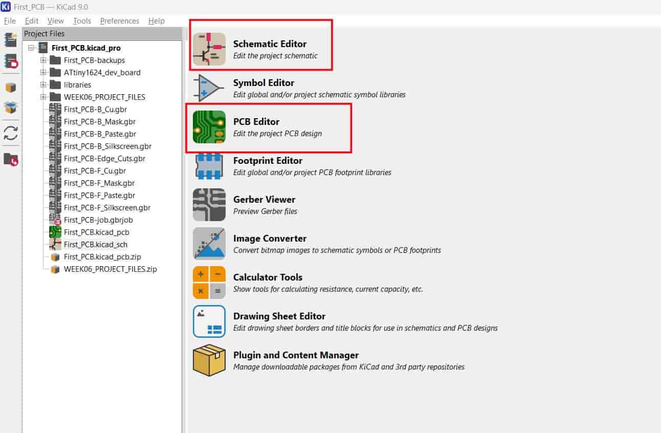
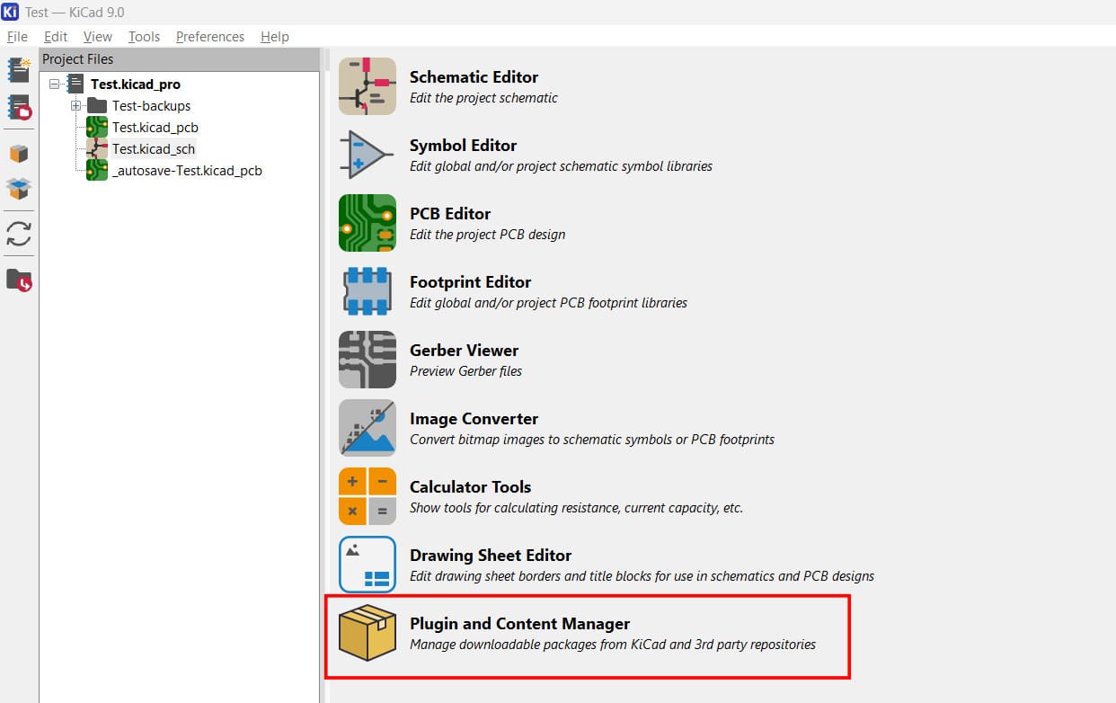
Introducing KiCad and Creating a New Project
KiCad is split into a few main tools: the Schematic Editor (Eeschema) for capturing the circuit logic, the PCB Editor (PCBNew) for laying out the physical board, and a 3D viewer for previewing the final result. Started by creating a new project, which generates a linked schematic (.kicad_sch) and PCB (.kicad_pcb) file pair.
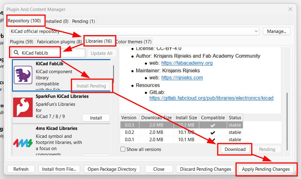
Installing the Fab Library
Opened the Plugin and Content Manager, searched for "KiCad FabLib", then downloaded, installed, and applied the pending changes so the Fab Lab–specific symbols and footprints became available in the library list.
Library reference: KiCad FabLib
Schematic
Adding a Symbol
To add a component symbol, clicked the diode icon in the right-hand toolbar to open the symbol picker and searched for the parts used in this design.
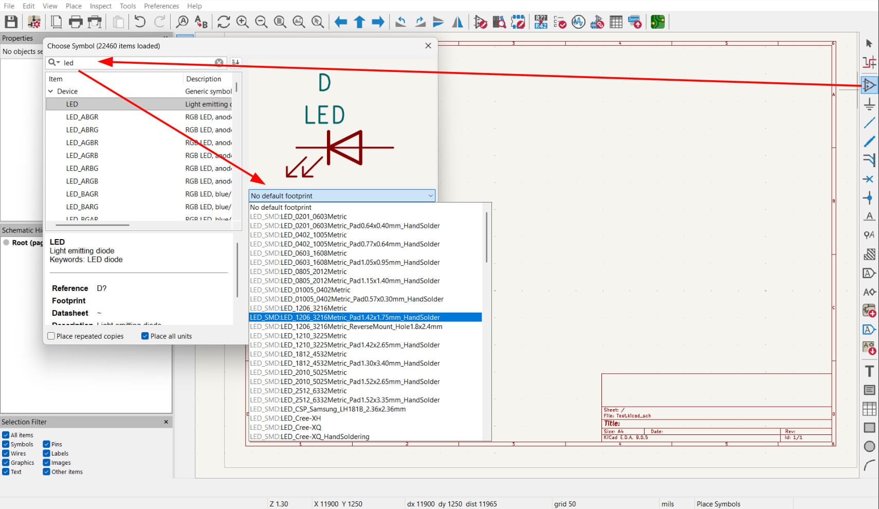
Adding a symbol from the Fablab Library is shown below.
.jpg)
ATtiny412 Pinout Diagram
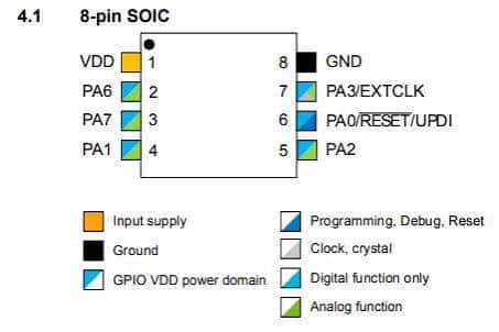
Reference pinout used for placing the ATtiny412 in the schematic, sourced from Microchip's official datasheet: ATtiny212/214/412/414/416 Datasheet (Microchip).
Connecting Symbols with Wires
Drew wires between component pins in the schematic editor to define the electrical connections between symbols.
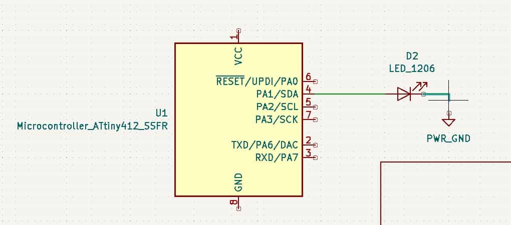
LED Resistor Calculation
Calculated the correct series resistor value for each LED using a standard LED resistor calculator: DigiKey LED Series Resistor Calculator. This takes the supply voltage, LED forward voltage, and desired current to give the resistor value needed to protect the LED.
.jpg)
Adding Values to Components
Assigned the calculated values to each component in the schematic — particularly the LED series resistors — so the design intent is captured directly in the schematic rather than left blank.
.jpg)
Adding Global Labels
Used net labels instead of drawing long wires across the whole sheet, keeping the schematic clean and readable while still defining the logical connections between components.

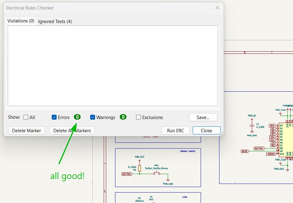
ERC — Electrical Rule Check
Ran ERC to confirm there were no electrical errors (unconnected pins, conflicting drivers, etc.) in the schematic before moving to layout.
.jpg)
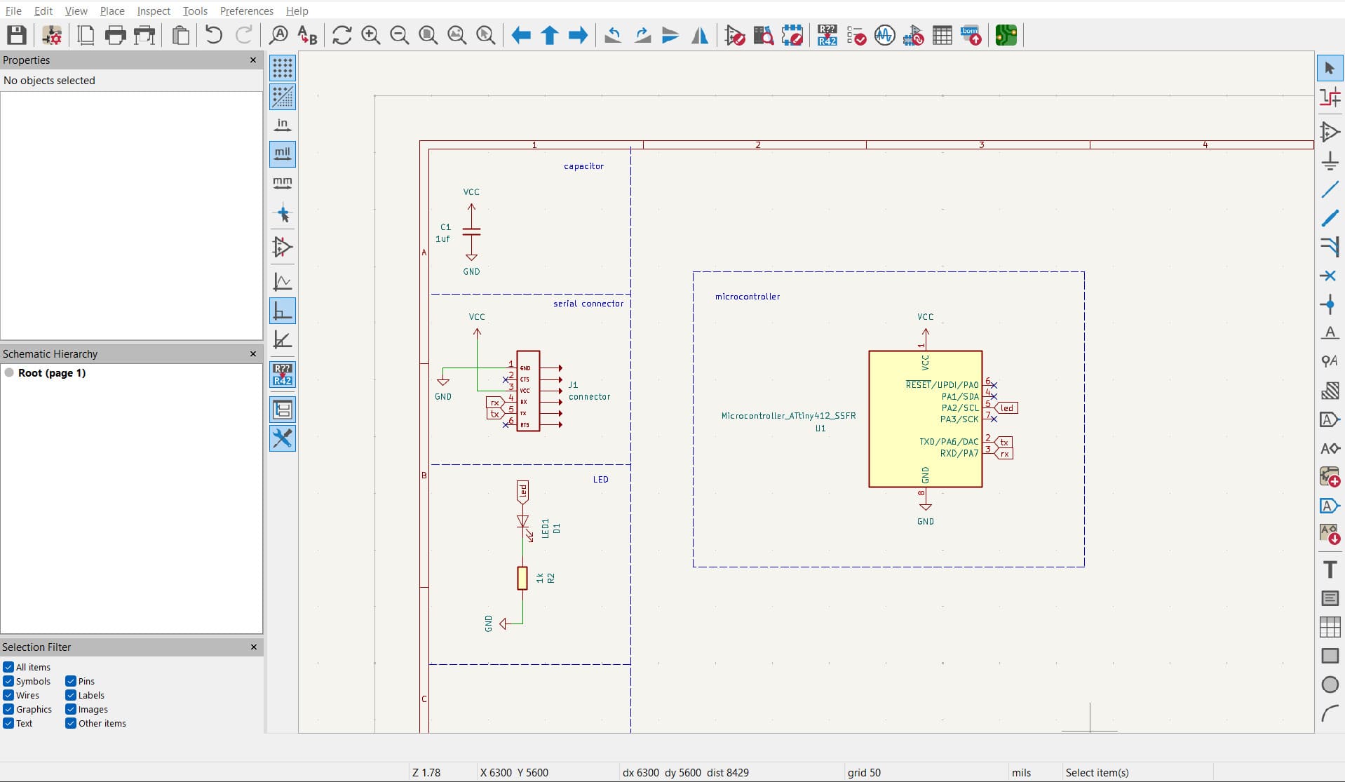
Organizing the Schematic
Rearranged components and labels for better readability — grouping related parts together and keeping the layout logical so the schematic is easy to follow for documentation purposes.
.jpg)
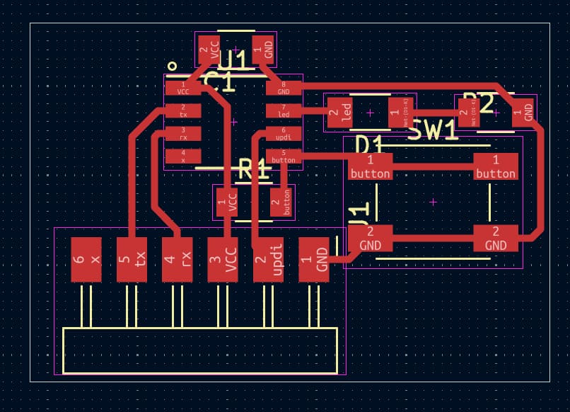
Final Schematic Diagram
PCB Layout
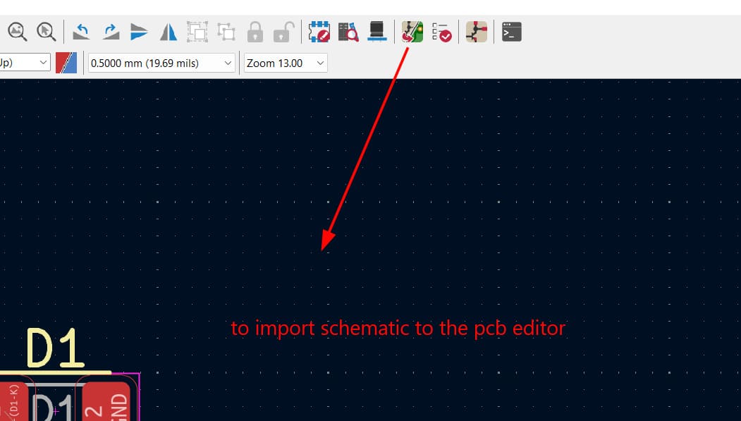
Updating from Schematic to PCB Editor
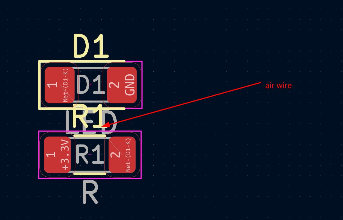
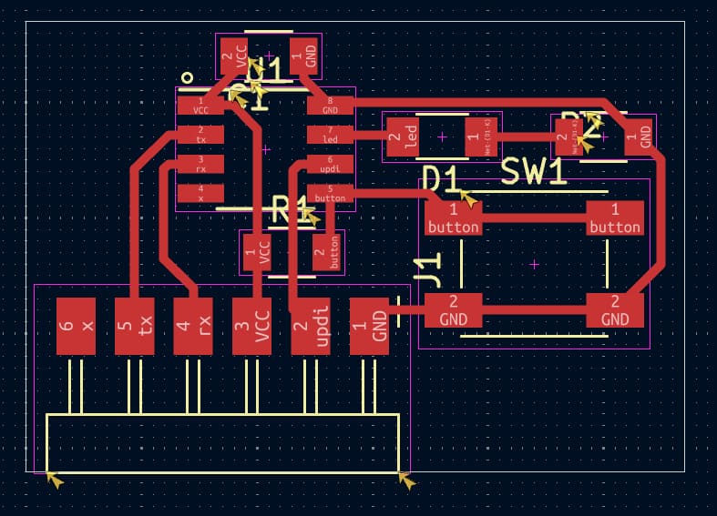
Once the schematic was complete, switched to the PCB editor to convert it into a physical board layout. This pulls all schematic components and their connections (ratsnest) into the PCB view.
The blue lines shown are air wires (ratsnest) — they represent the logical connections from the schematic that haven't yet been routed as physical copper traces.
Arranging Components for Better Placement
Repositioned components on the board for a more efficient and manufacturable layout — focusing on minimizing trace lengths and keeping related parts close together.
.jpg)
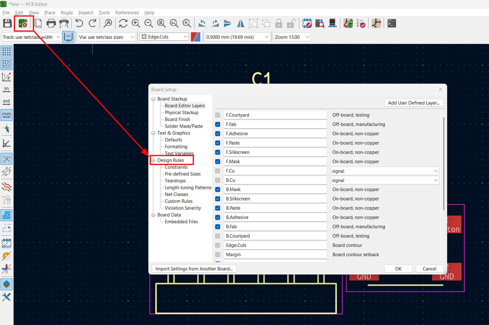
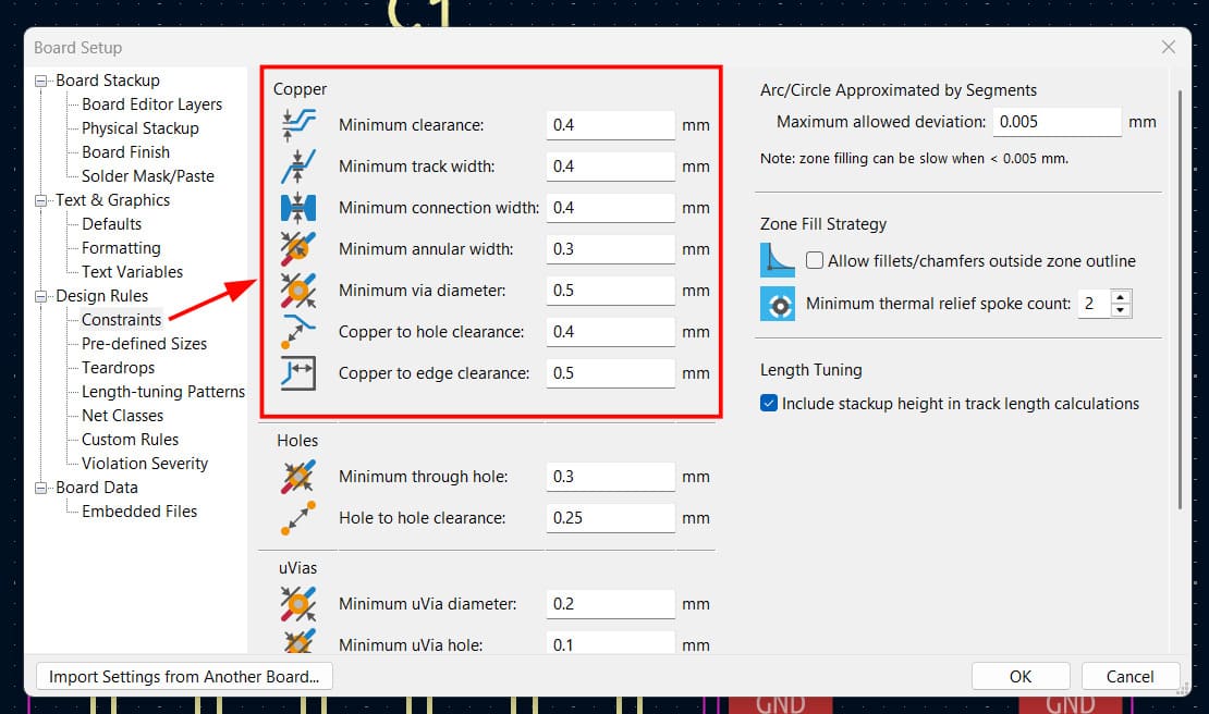
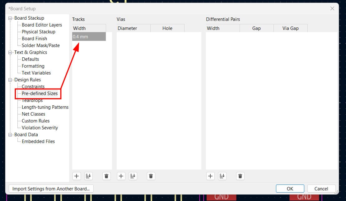
Design Rule Setup / Board Setup
Went to Board Setup and configured the design constraints to match the PCB etching machine's capabilities, setting all clearance and trace-width values before starting layout so the board stays within what the machine can physically produce. 0.4mm is the standard trace width used at the Fab Lab.
Drawing a Wire Between Pads
Routed connections using Route → Route Single Track (shortcut: X). To select an entire trace, clicked any part of it then pressed U to select the full connected path. Kept all traces at 45° angles for clean, reliable etching.
.jpg)
Above was just an example of the routing process. Now, I have updated the PCB from the schematic and routed all components as shown below.
Used a zero-ohm resistor — essentially a wire in resistor form — to jump over another trace where routing got tight.
Edge Cut Drawing
Selected the Edge.Cuts layer in the Appearance panel and drew a rectangle around the components to define the physical outer edge of the PCB.
.jpg)
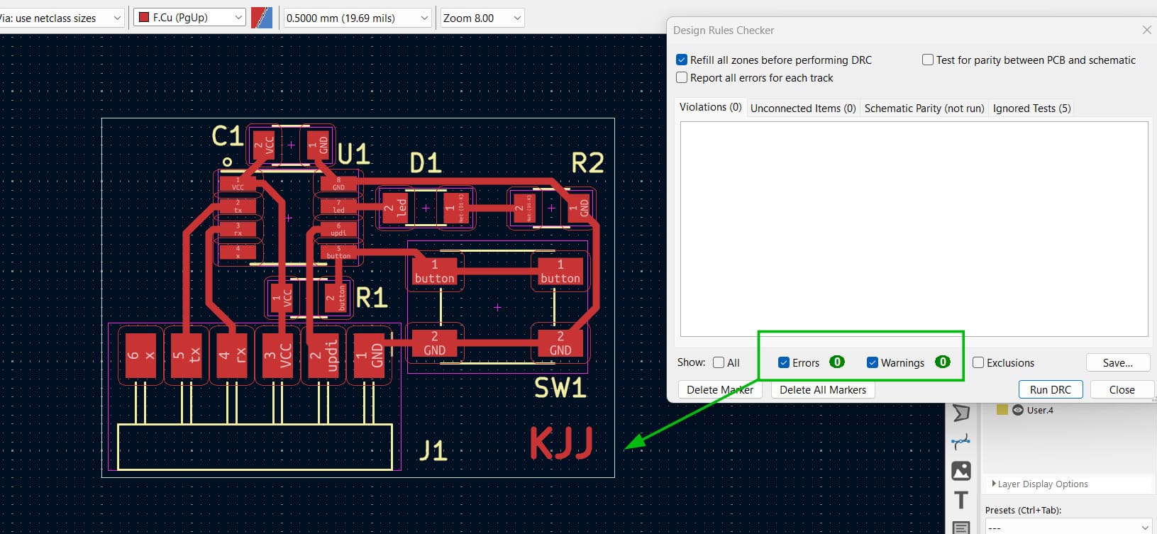
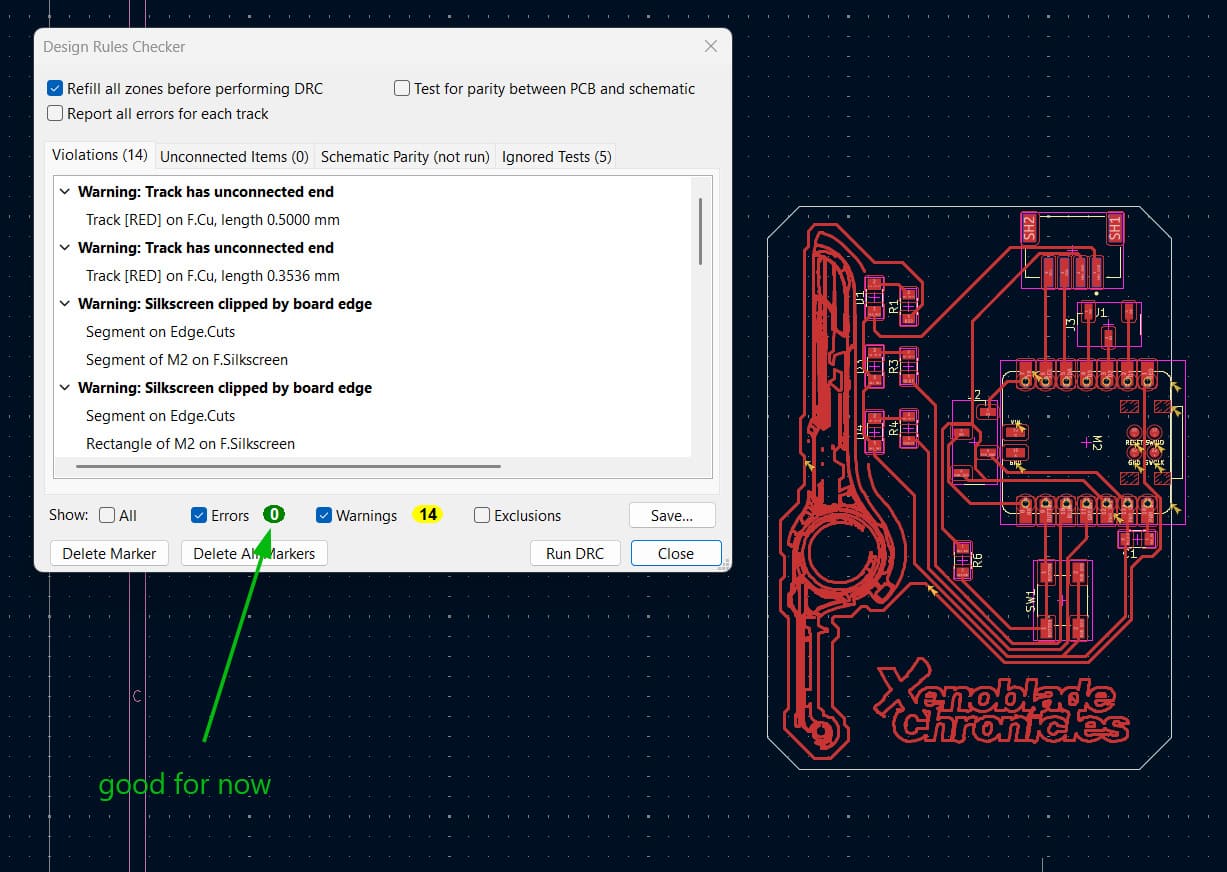
DRC Check — Design Rule Check
Ran DRC to validate the board. The first pass returned a couple of errors — one for overlapping components and one for a trace too close to the board edge. Fixed both and re-ran until clean.
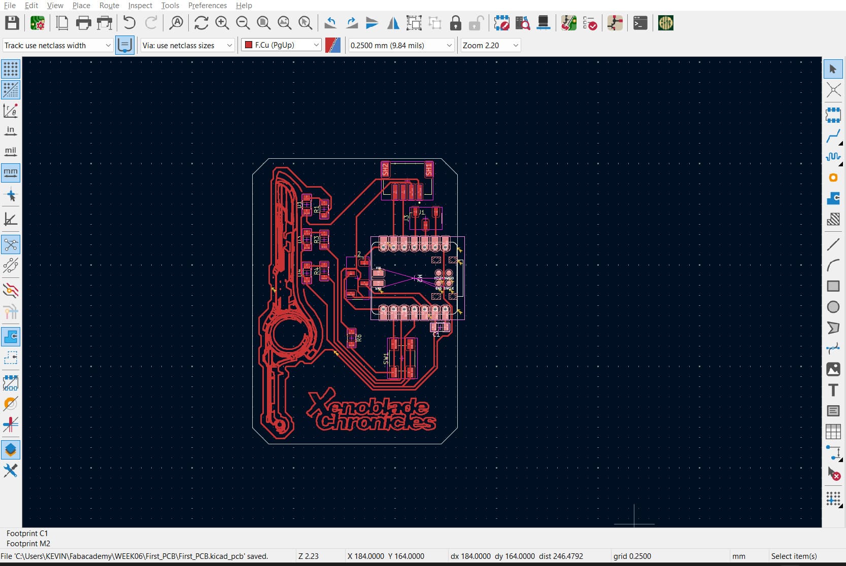
Final PCB Layout
After correcting all DRC errors we get the final PCB layout.
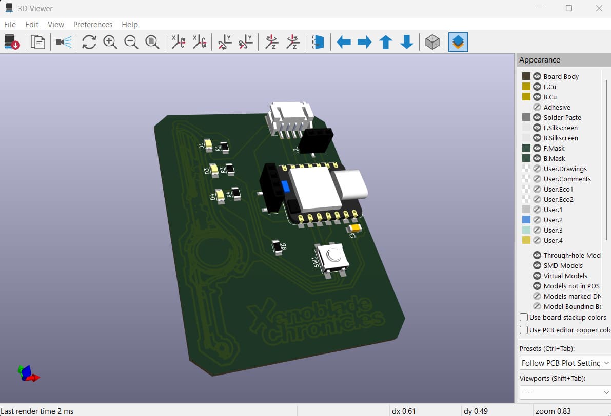
3D PCB Output
Once the board layout was complete, opened it in the 3D viewer to see a rendered preview of the final PCB — including the solder mask, silkscreen, and 3D component models.
.jpg)
On a real PCB, the green coating is the solder mask — it insulates and protects the copper traces, only exposing the pads where components need to be soldered. The white text and markings on top are the silkscreen, used for labels, component outlines, and pin indicators.
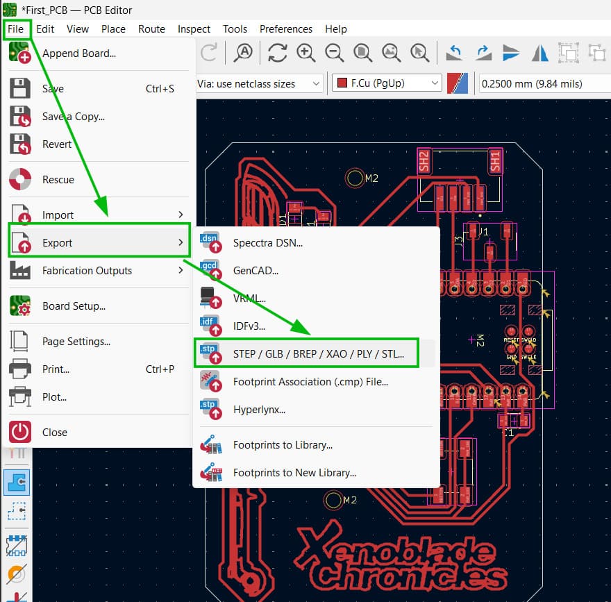
Gerber Export
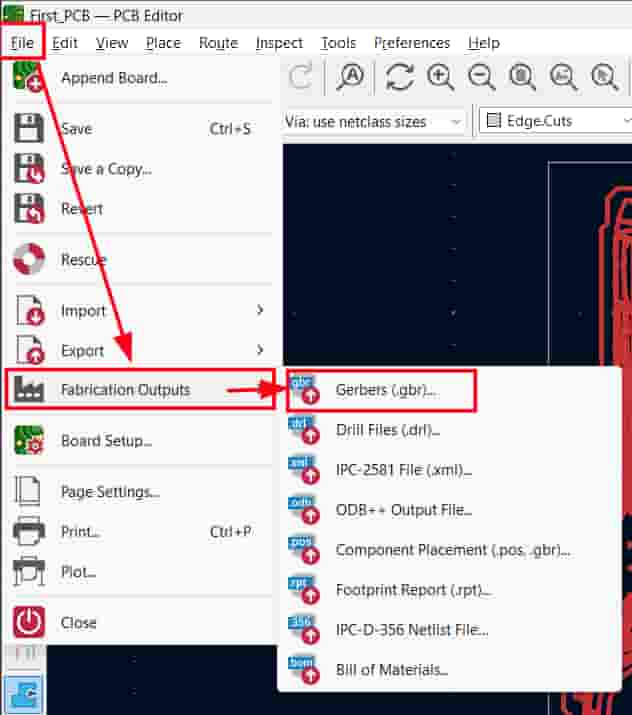
To export the manufacturing files, went to File → Fabrication Outputs → Gerbers.
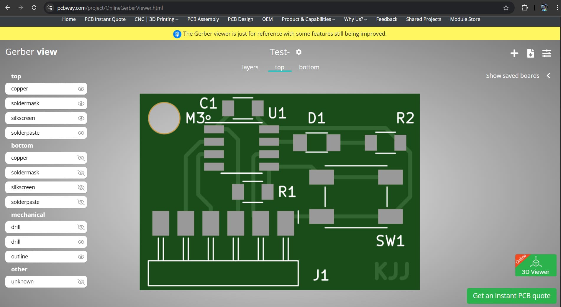
Exported the Gerber files and uploaded them to PCBWay's Gerber viewer to preview the board visually before ordering — confirming the trace layout, drill holes, and board outline all looked correct.
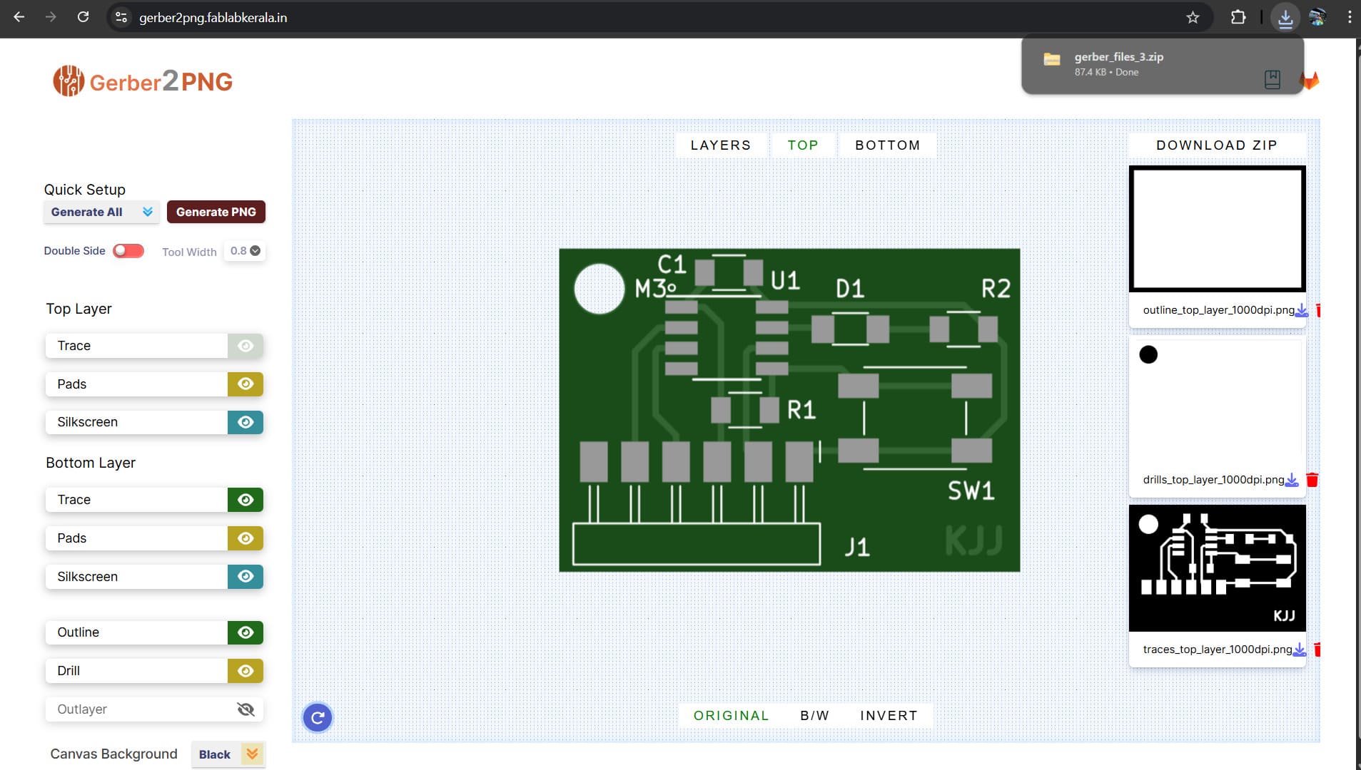
For boards milled in-house, the Gerber files are run through a tool that generates a trace image — a PNG the milling machine uses to etch away copper from the blank PCB.We use a website called gerber2png.
Your Custom XIAO PCB
XIAO Pinout Diagram
.jpg)
Reference pinout for the Seeed Studio XIAO module used in this design, sourced from the official Seeed Studio Wiki: Seeed Studio XIAO ESP32C6 Wiki.
Importing an External Library from SnapEDA
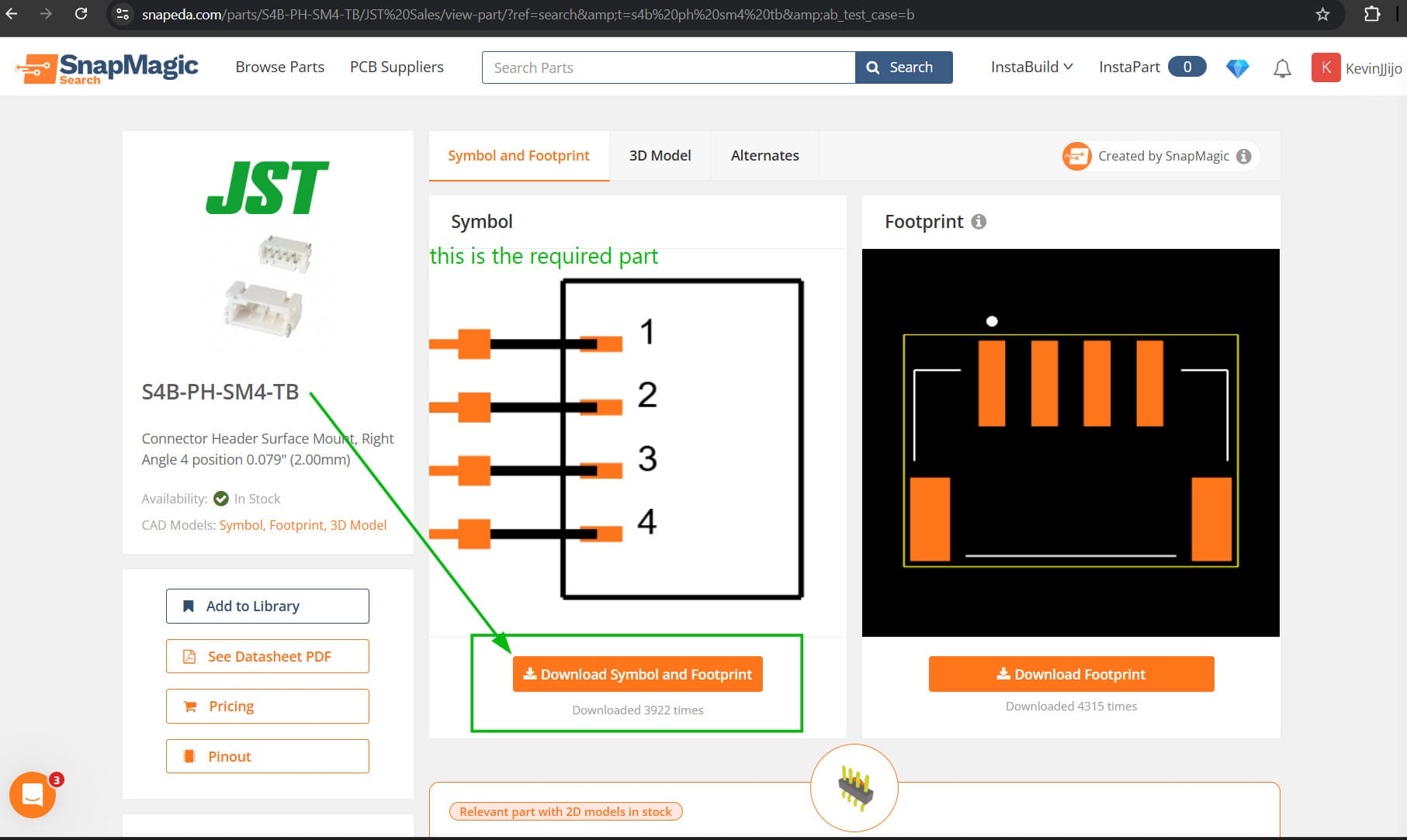
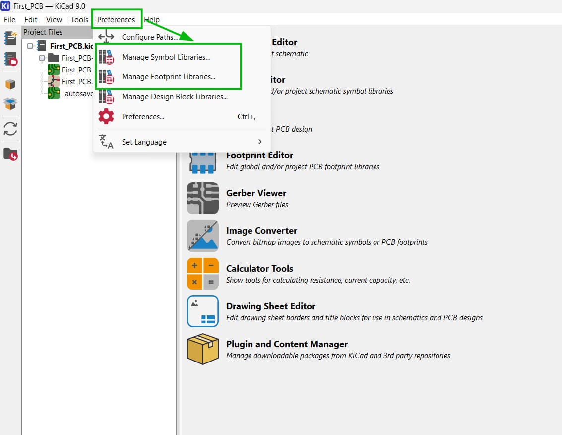
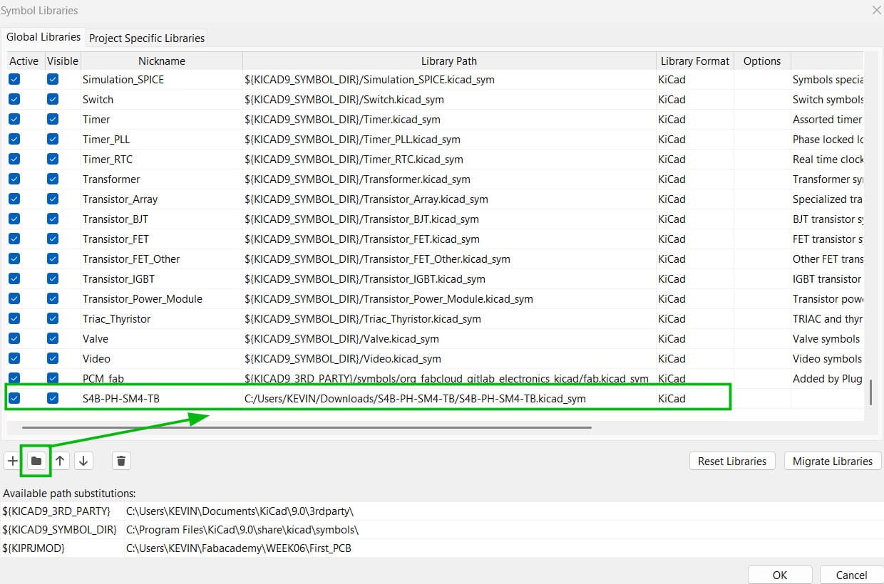
Not every part needed for this board exists in KiCad's default libraries, so used SnapMagic/SnapEDA to download free symbols, footprints, and 3D models for the missing components.
Went to SnapEDA and searched for the part needed — in this case a 4-pin right-angle SMD JST header, part number S4B-PH-SM4-TB.
The downloaded zip contains:
- .kicad_sym — schematic symbol
- .kicad_mod — PCB footprint
- .step — 3D model
To add them into KiCad: Preferences → Manage Symbol Libraries and Manage Footprint Libraries, linking each to its file location. For the footprint library, the entire folder is added rather than individual files.
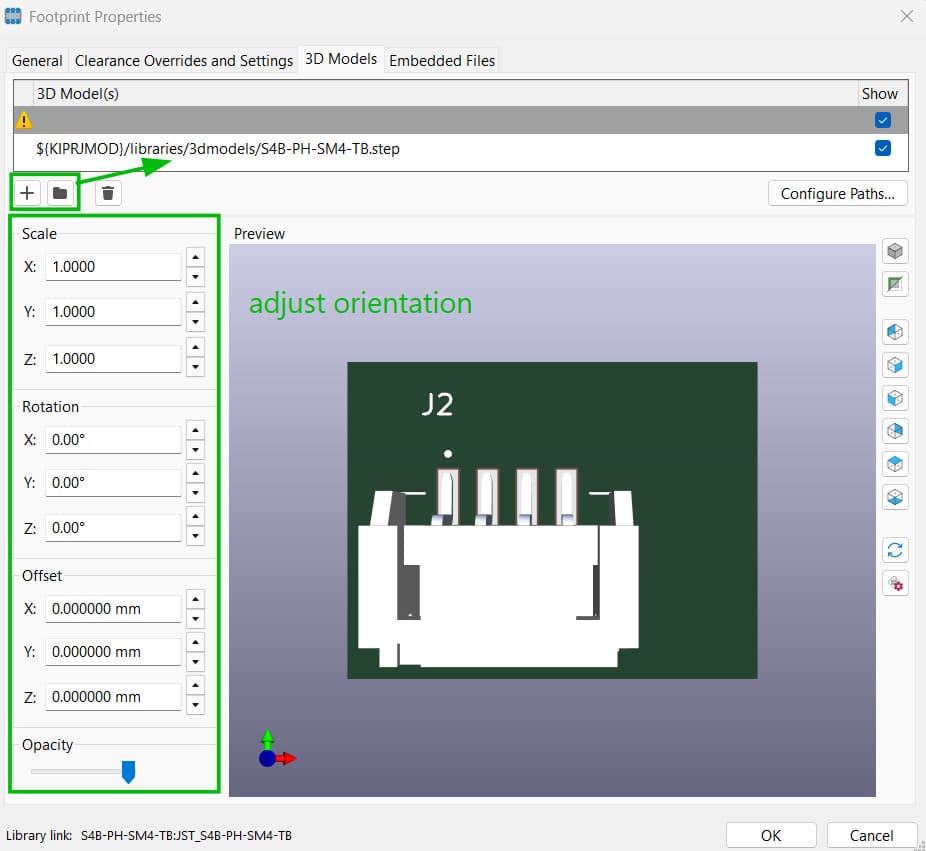
To attach the 3D model: double-click the part in the PCB editor, go to the 3D Models tab, and add the path to the .step file (ideally stored in the project folder under libraries/3d models). It almost never positions correctly by default, so the offset and rotation controls are used to manually align it onto the footprint using the pin holes as reference.
Other connector types considered during this process:
- Header pin — soldered directly onto the board, 2.54mm pitch (standard, breadboard compatible)
- JST connector — better fit and more secure than a plain header. Seeed Studio's I²C JST is 2mm pitch, horizontal orientation only, so the footprint had to be added to the library manually
- USB-C — an example of a horizontal connector with an overhang/pivot-style mount
- Terminal block — 3mm or 5mm pitch
Auto Routing: set all trace width and clearance values under Net Classes before running. Differential pairs (e.g. USB D+/D−) are two traces that must be kept the same length. Press V to place a via and jump a trace between copper layers.
Schematic — Custom XIAO PCB
First designed all the circuits in the schematic editor for the custom board.
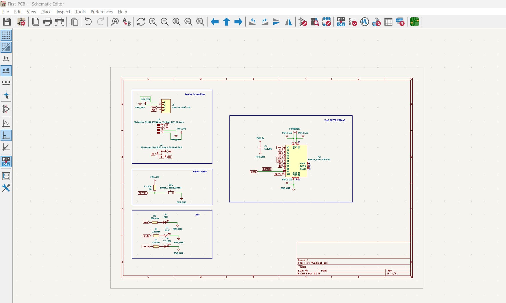
Ran ERC to confirm there were no errors.
PCB Layout — Custom XIAO PCB
Switched to the PCB editor and made all the traces — focused on the communication traces first and kept them short to minimize noise, then connected the remaining GPIO traces as second priority.
Adding Name and Graphics
In Inkscape, designed the Monado sword outline from Xenoblade Chronicles — since this is a simple PCB, wanted it to have some personal meaning. Exported it as an SVG, then imported it into Fusion 360 (since KiCad needs a DXF for custom board outlines) and cleaned up the outline there to make sure it was a proper closed path so it would export correctly to DXF.
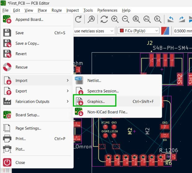
In KiCad, imported the DXF as a graphic via File → Import → Graphics, making sure to place it onto the Front Copper layer so the milling machine knows to cut it out.
I play a lot of Super Smash Bros, and one of the characters I main is Shulk from the Xenoblade Chronicles series.

Image Credits: Source
He wields a special sword called the Monado, where you can boost certain aspects like speed, power, and defence — the sword changes colour to indicate which mode is active.
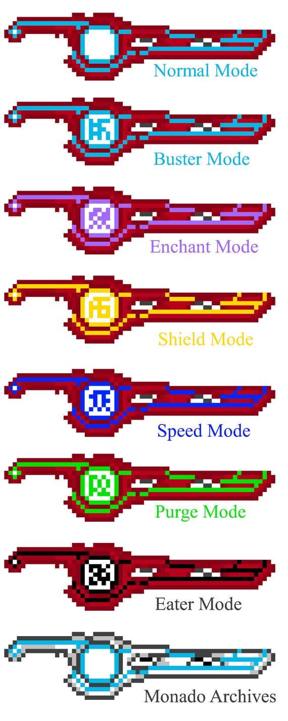
Image Credits: Source
Since the assignment was to design a PCB with an LED circuit and a switch, I made it so the LEDs show which mode has been chosen for Shulk to fight with.
Tested all connections using DRC — no errors.
Since this is a trial PCB, all communication interfaces were broken out to jumper headers so everything stays accessible for testing:
UART (Serial)
- TX → D6 (GP0)
- RX → D7 (GP1)
- Grouped these 2 pins + GND + 3V3 into a 4-pin header (standard FTDI layout)
I²C
- SDA → D4 (GP6)
- SCL → D5 (GP7)
- Grouped with GND + 3V3 into a 4-pin header (matches Stemma QT / Qwiic convention)
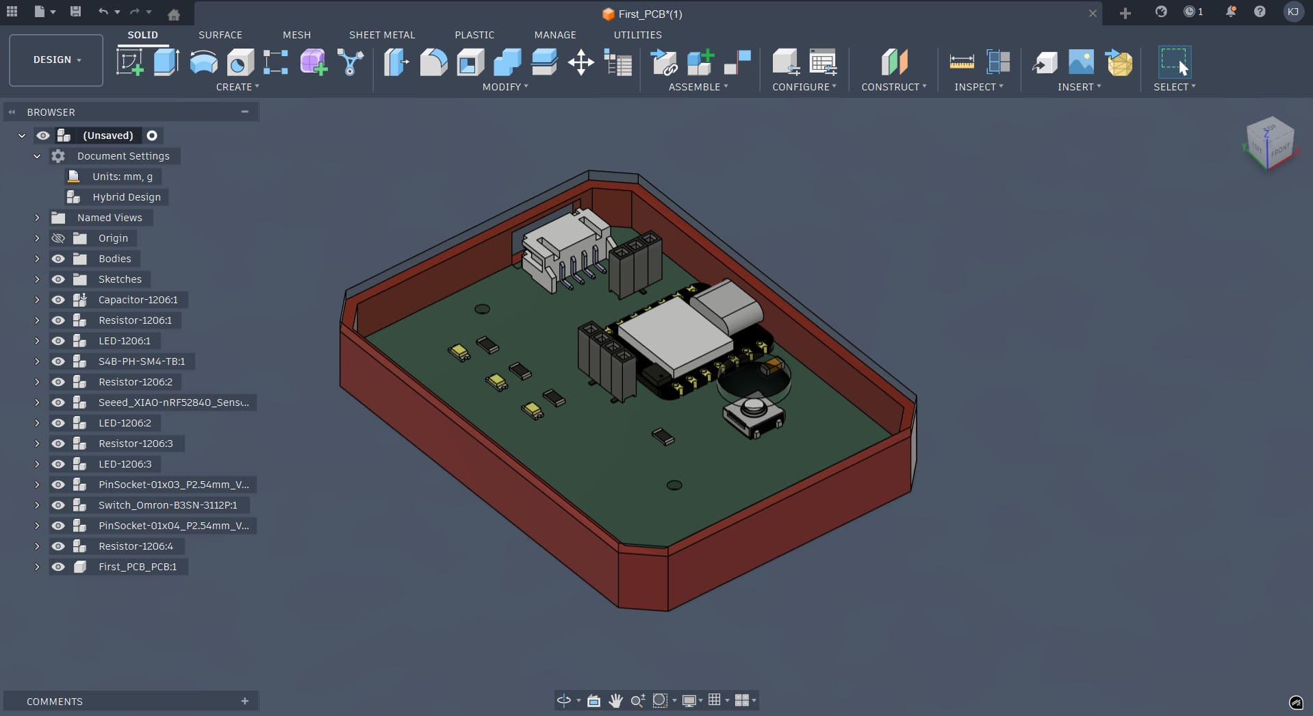
Exporting 3D File — Custom XIAO PCB
The 3D model of the PCB came out looking great.
To export the Gerber files: File → Fabrication Outputs → Gerbers.
To export the 3D model: File → Export → Step.
Designing the Enclosure
Exporting the 3D File and Importing to Fusion 360
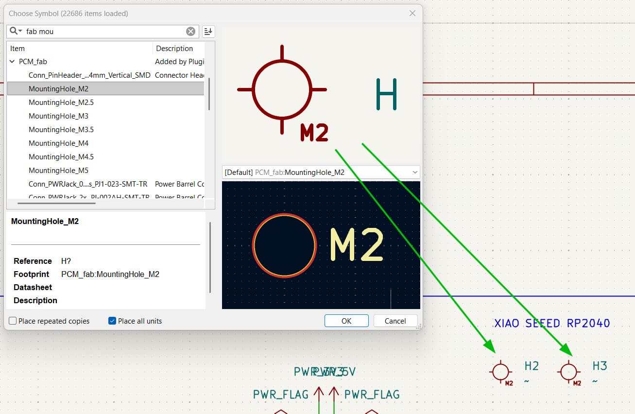
To mount the PCB inside the case, first added mounting holes in the schematic editor by placing them as components, then routed them through to the PCB layout — giving two holes in the final output.
Imported the exported STEP file of the PCB into Fusion 360 and designed a case around it, leaving holes for the XIAO Seeed RP2040 and the I²C header pins, plus a small hole on the top clear acrylic layer so the switch can be clicked.