Group assignment
Here is the link to the group assignment.About the Machine
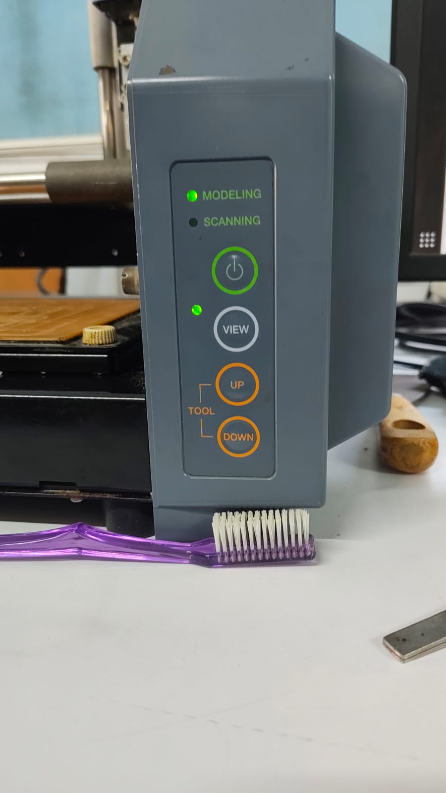
We are using the MDX-20 3D Milling Machine is a compact desktop CBC milling machine that has been modified to mill PCBs with high precision in our lab.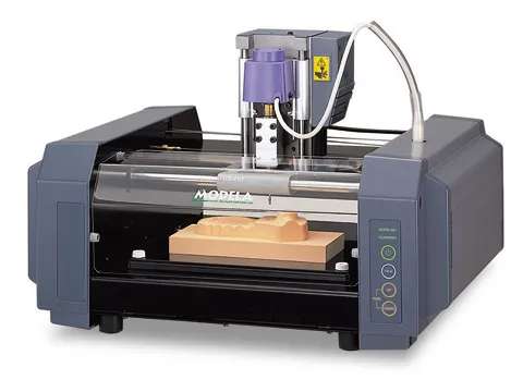
Individual assignment
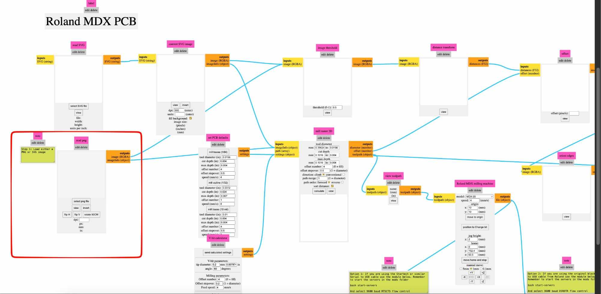
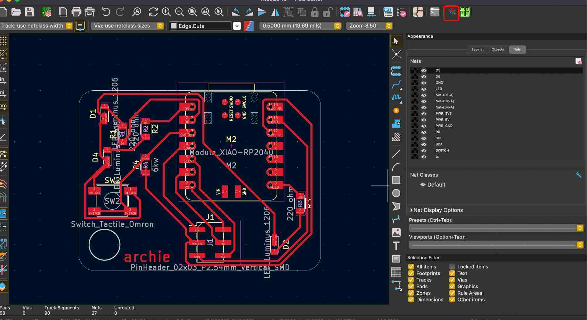
So this week's individual assignment was to make and test an embedded microcontroller that we designed ourselves. Since I had already designed my PCB board back in Week 6, i decided to test it out here.Setting Up the Plugins in KiCad
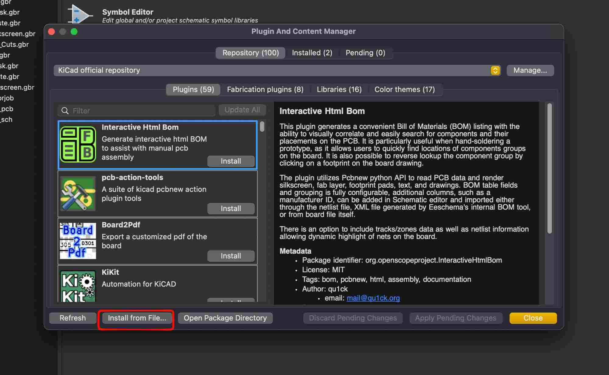
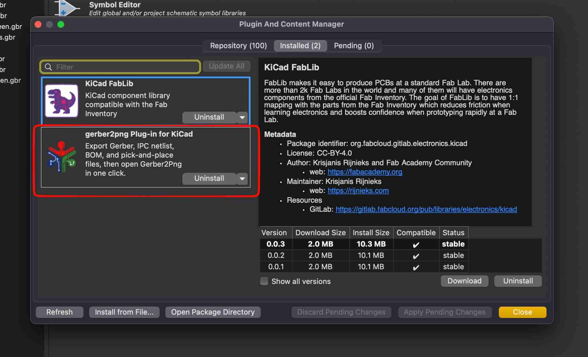
Before jumping into anything, the first thing we do at FabLab Kochi is make sure two key plugins are installed in KiCad:
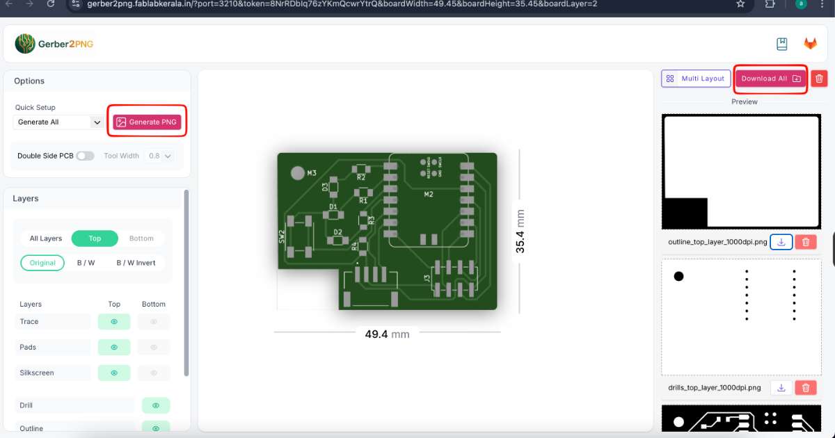
1. Gerber to PNG Plugin – This plugin is used to convert gerber files to PNG. I grabbed from a Github link and installed directly to KiCad
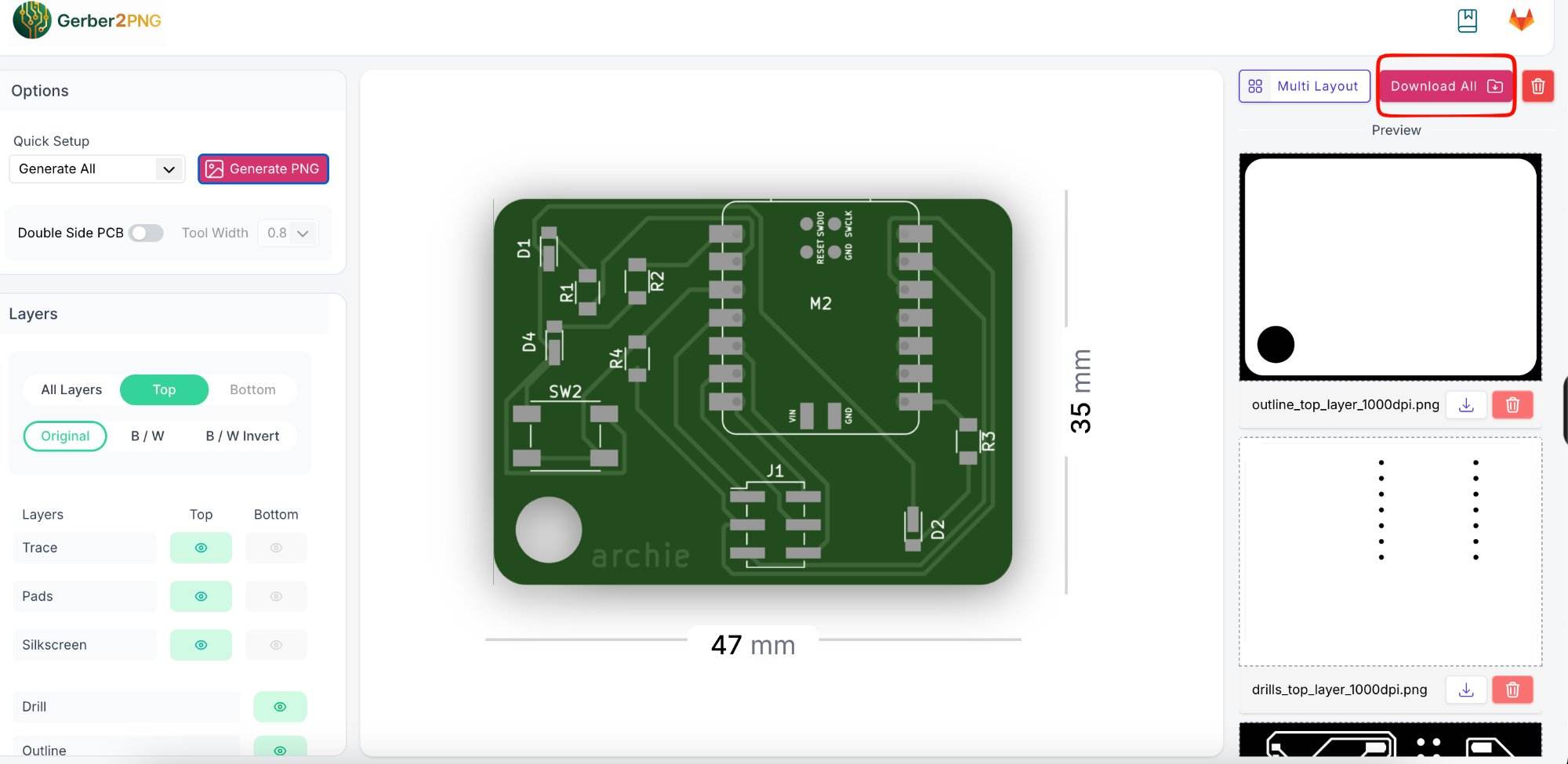
This is the gerber file whuch the plugin generates.
 You can also get this live on our gerber2png website.
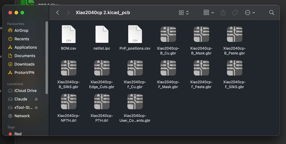
Here, you can either download everything at once or pick individual segments, whatever works for you.
 2. Interactive HTML BOM – a super handy plugin for bill of materials.
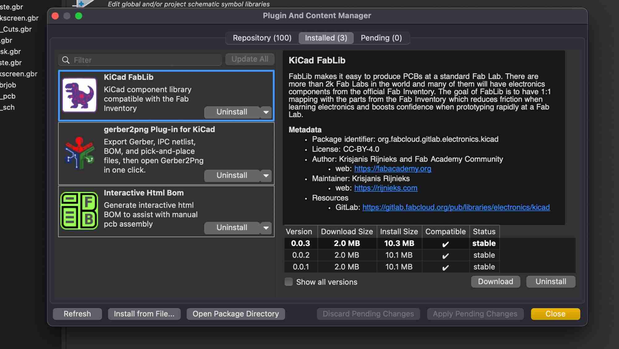 Once the plugins are in place, you click on the Interactive HTML BOM icon on the top tool bar. A popup appears, and you hit the "Generate BOM" button.
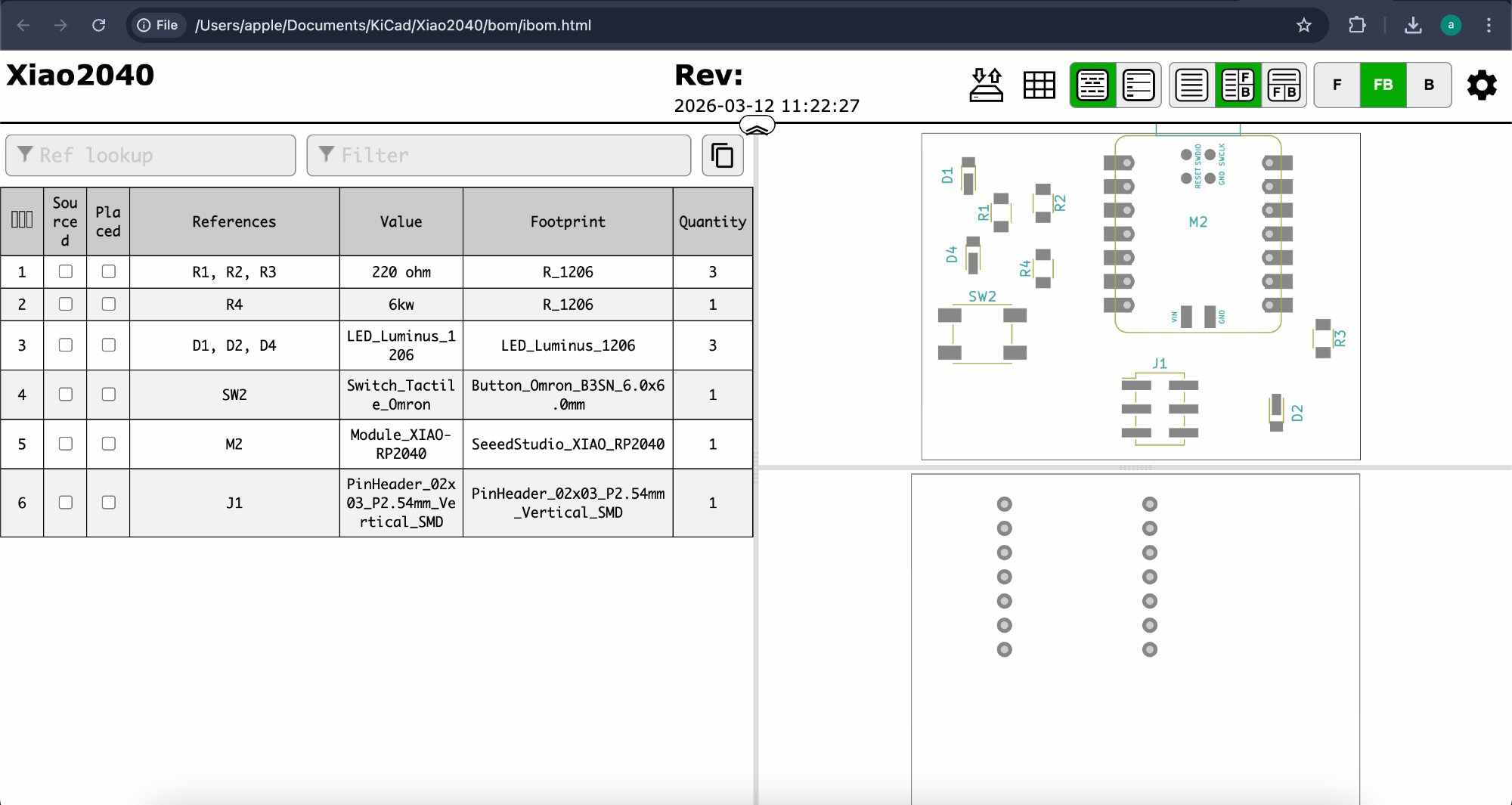
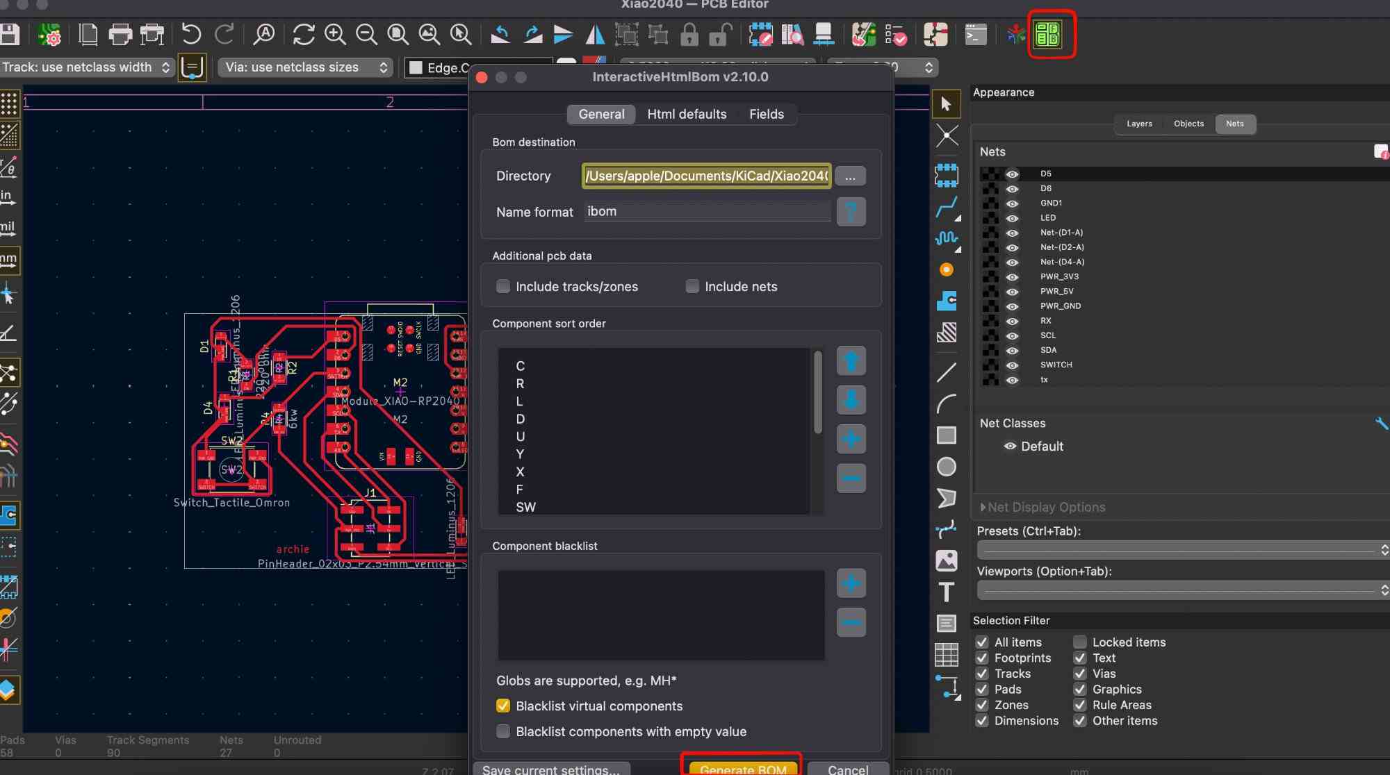 This opens up a neat page that shows:
All the component references on your PCB
A detailed datasheet-style chart of every component used
A handy checklist with quantities
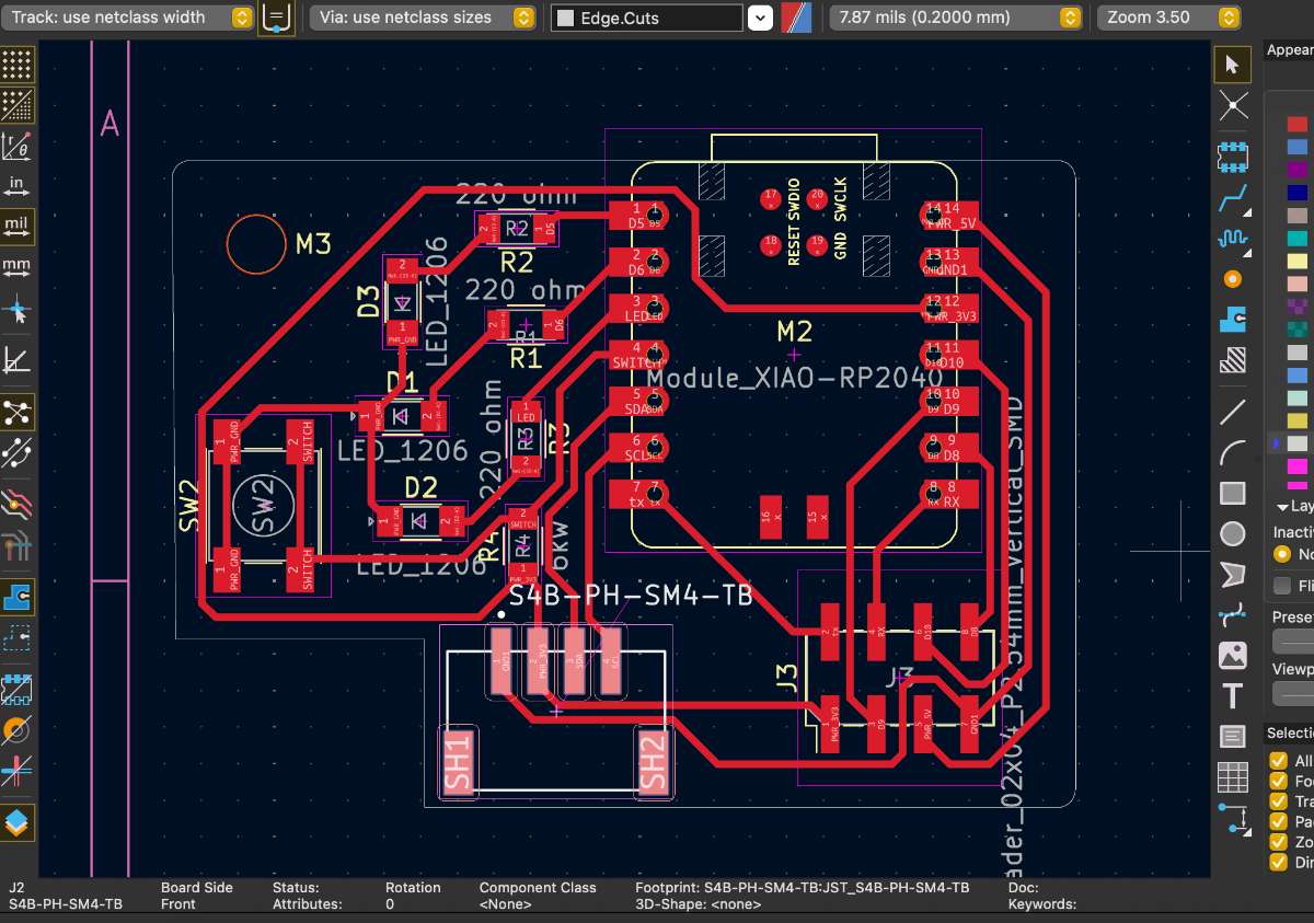
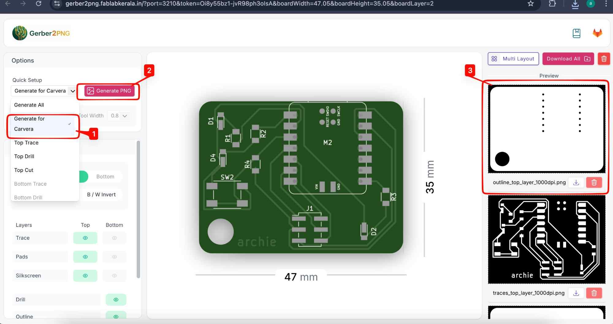
 The PCB design i used for milling is different from the above. The one above is just for reference. Below image consists of the PCB design which i used for production.
Milling the PCB
Online ModsTo send the file to the Roland we use Mods. from the 3 pngs previously downloaded u have to manually input it into the MODS.(For this, Our lab still uses the old version as it is more compatable with the version of windows we have)
 Meanwhile In the new online version of modes, you hit the View icon, It gives you the 3D preview of your PCB.
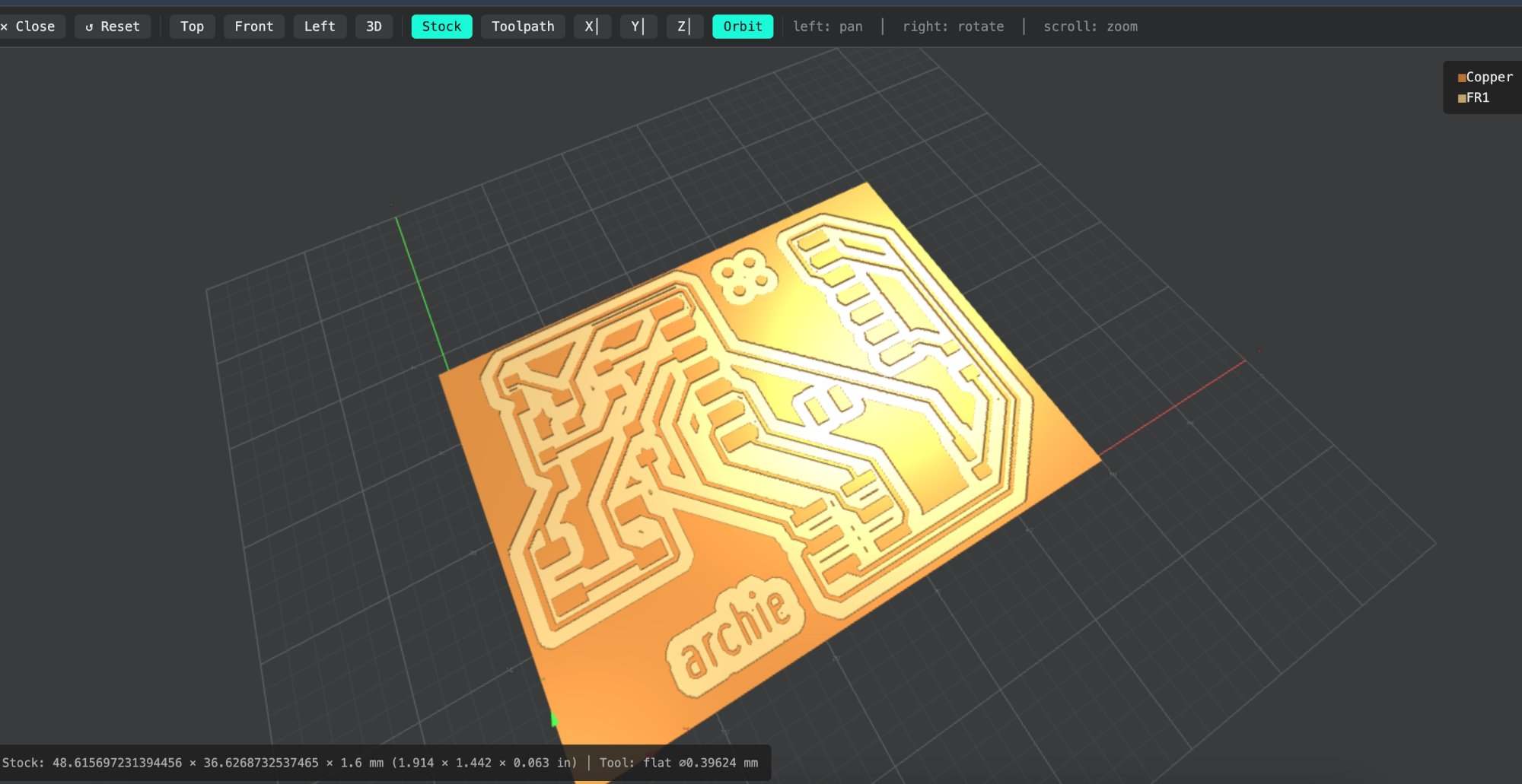 Then you click on Toolpath, which shows the exact path the milling tool will follow while cutting your PCB.
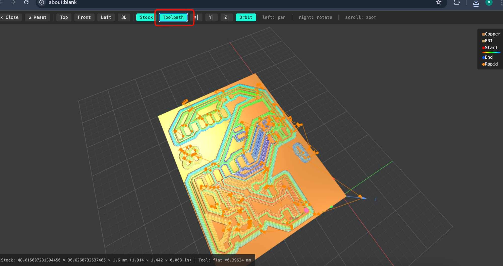
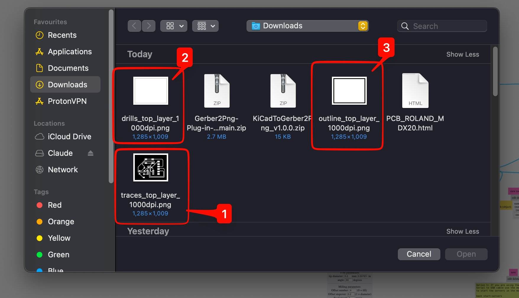
The following is the order in which you'll input the files.
1. Top Layer – the main circuit traces
2. Drill Layer – for all the holes
3. Outline Layer – the board cutout
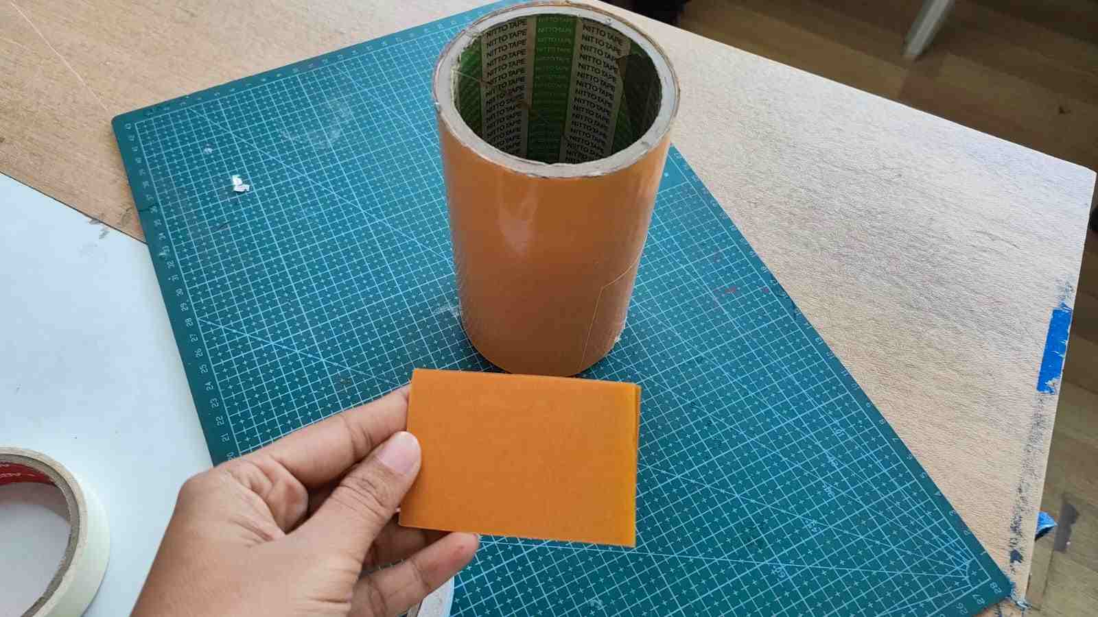
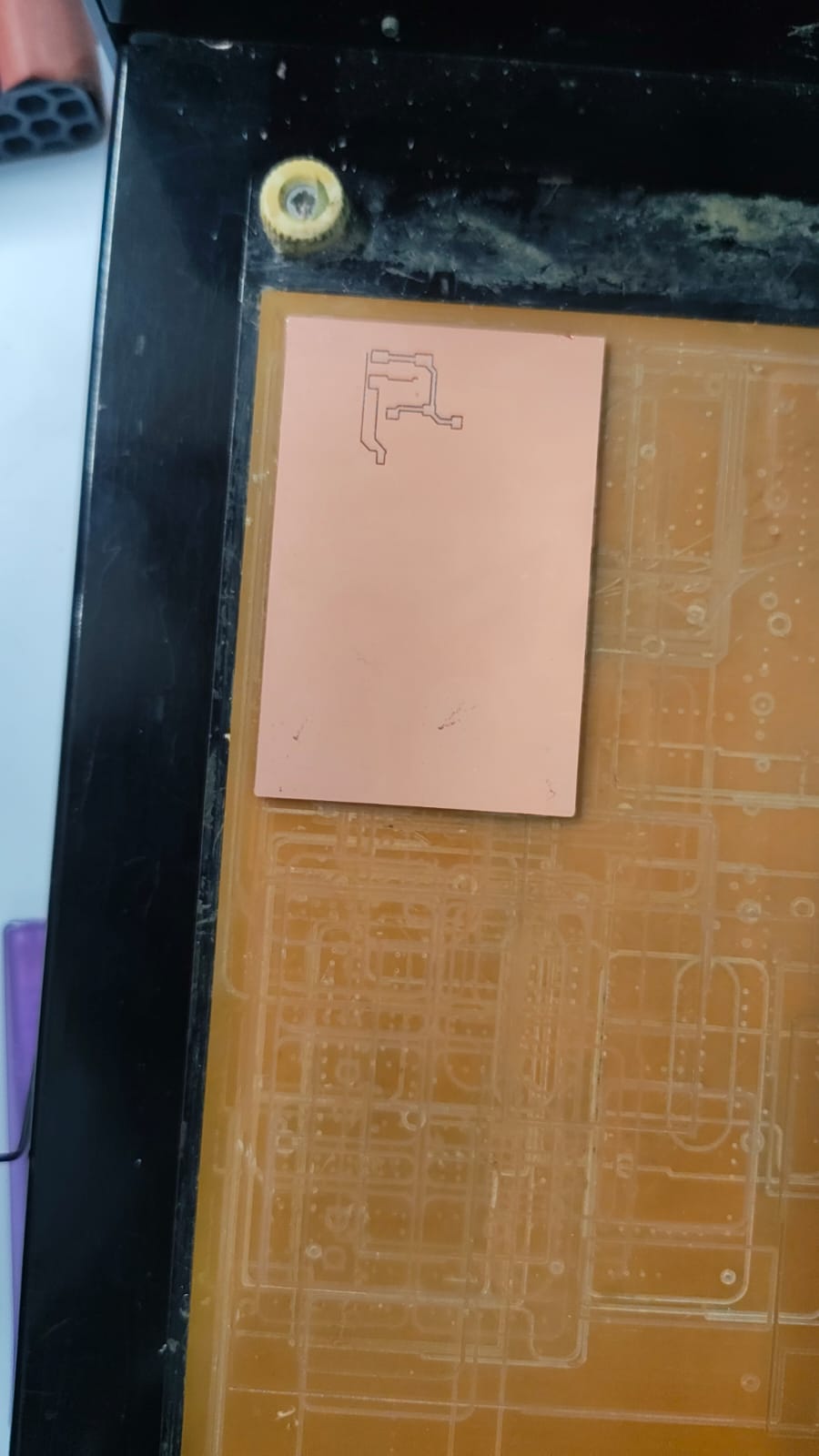
 After uploading the first png, make sure to stick the pcb onto the milling machine's bed, for that we stick a tape which transfers glue onto the FR1 PCB board.
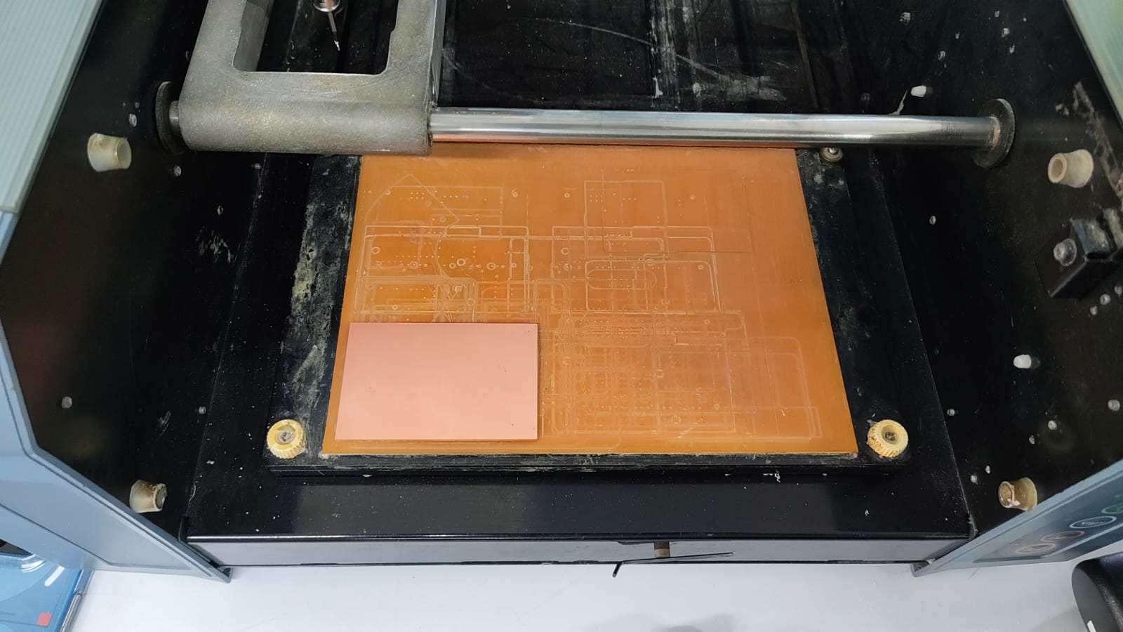 Here i have stuck the board a little inside the bed from both axis, then we have to manually measure the distance from the x axis of the bed and y axis of the bed to the x axis of the board and y axis of the board and enter the values into modes software.
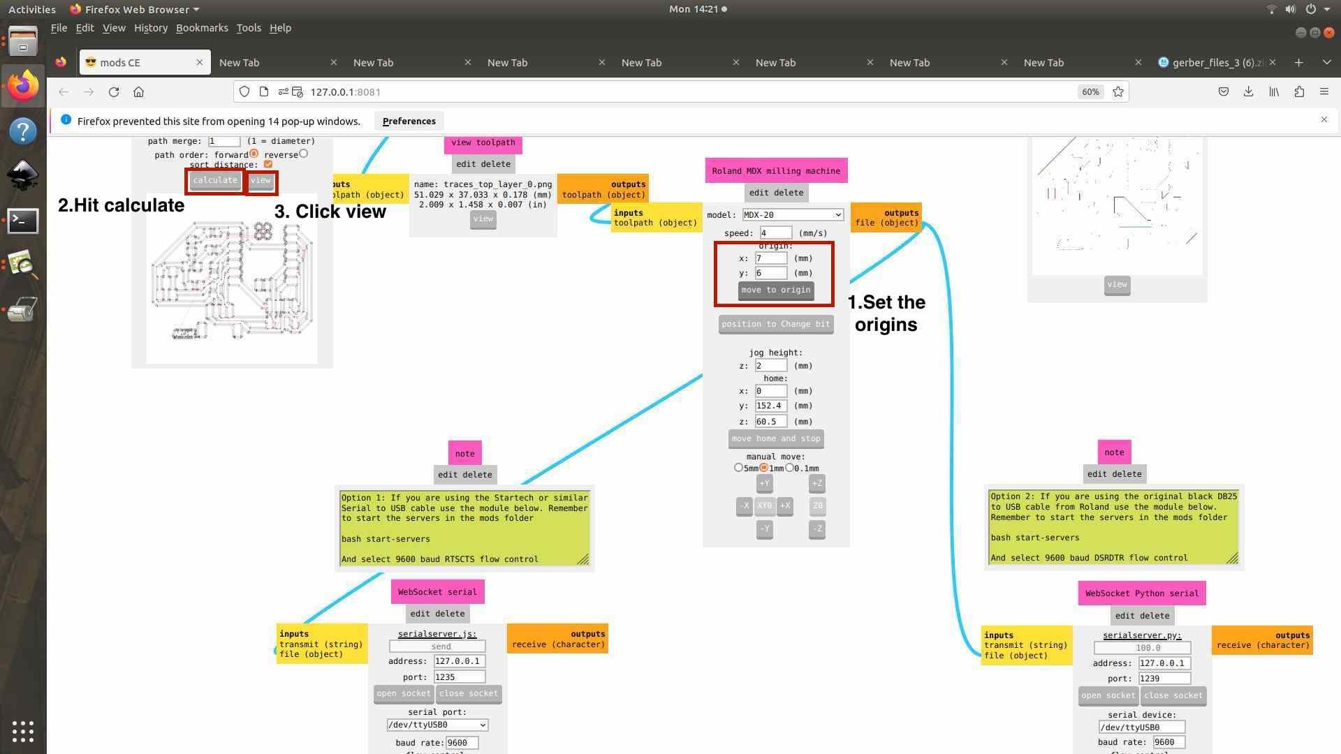 after clicking view we check if any of the traces are disrupted
 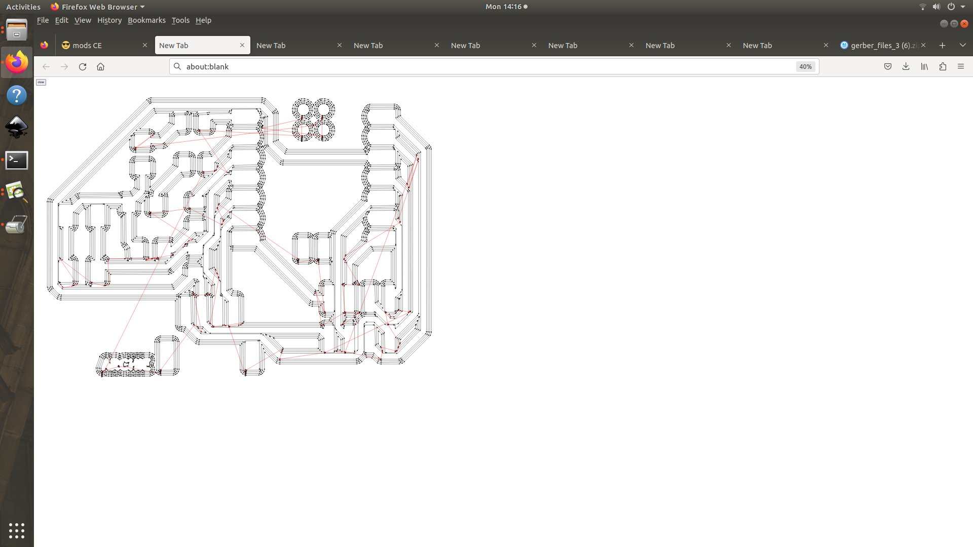 All good. Now click move to origin and the machine will move the bit to the mentioned axises
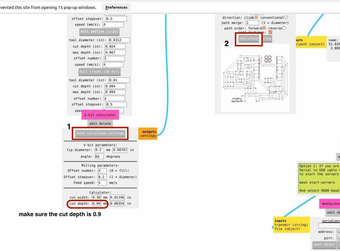
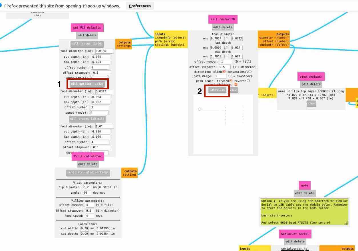
 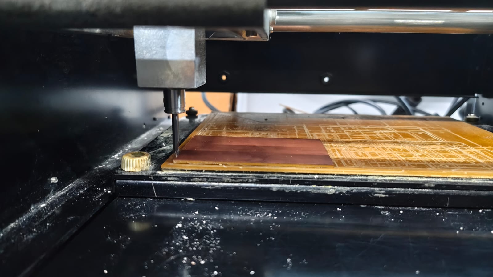 So now we move to the settings of the bit part, here, we are using a V bit of diameter 0.2mm, in the mods, follow the instruction on the image:
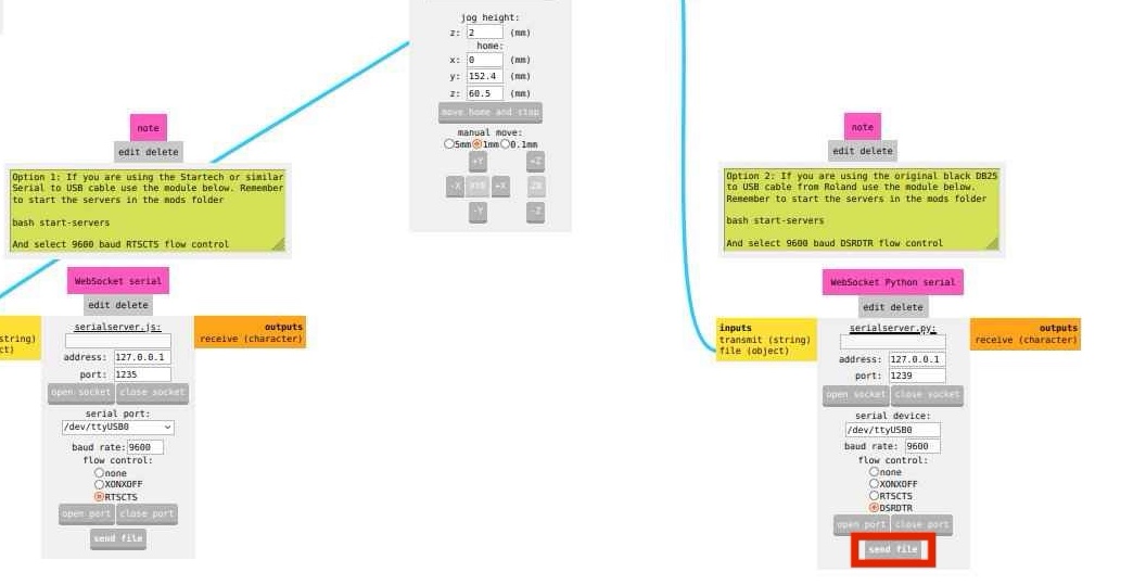
 After this we click on "send file" and the machine starts milling.
Also, remember to pause in between and check if all the traces are being milled, you can you this my clicking view button(which acts as a pause/resume button) on the machine.
Drilling the pcb
After the milling is done for the traces , change the uploaded PNG to the drilling one and then we have to change the Vbit with another bit more suitable for drilling, here we use a bit of diameter 0.8mm. to do so click on the "position to change bits" option on the software.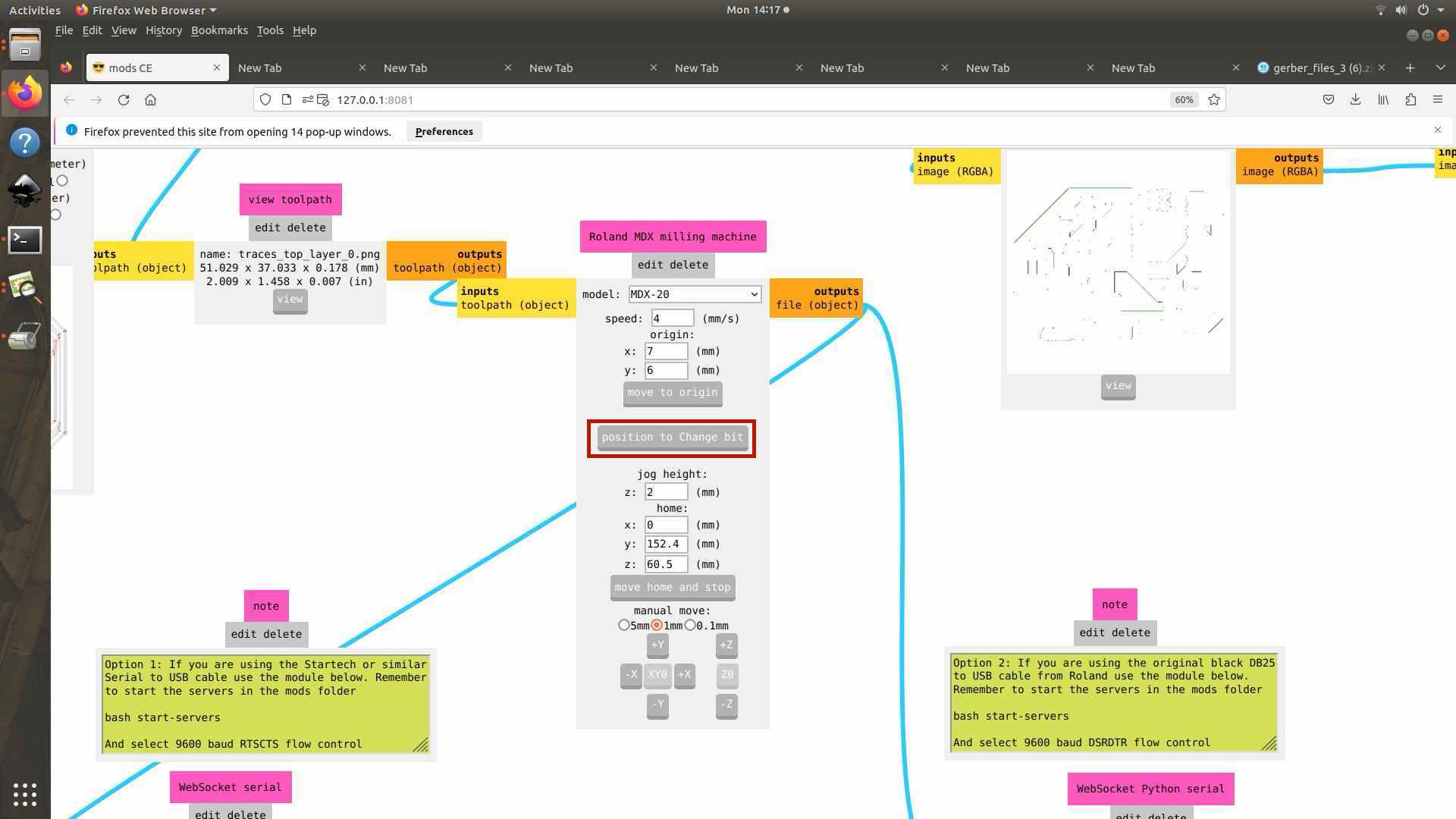 The bit will be moved to the centre and you can manually change the bit.
 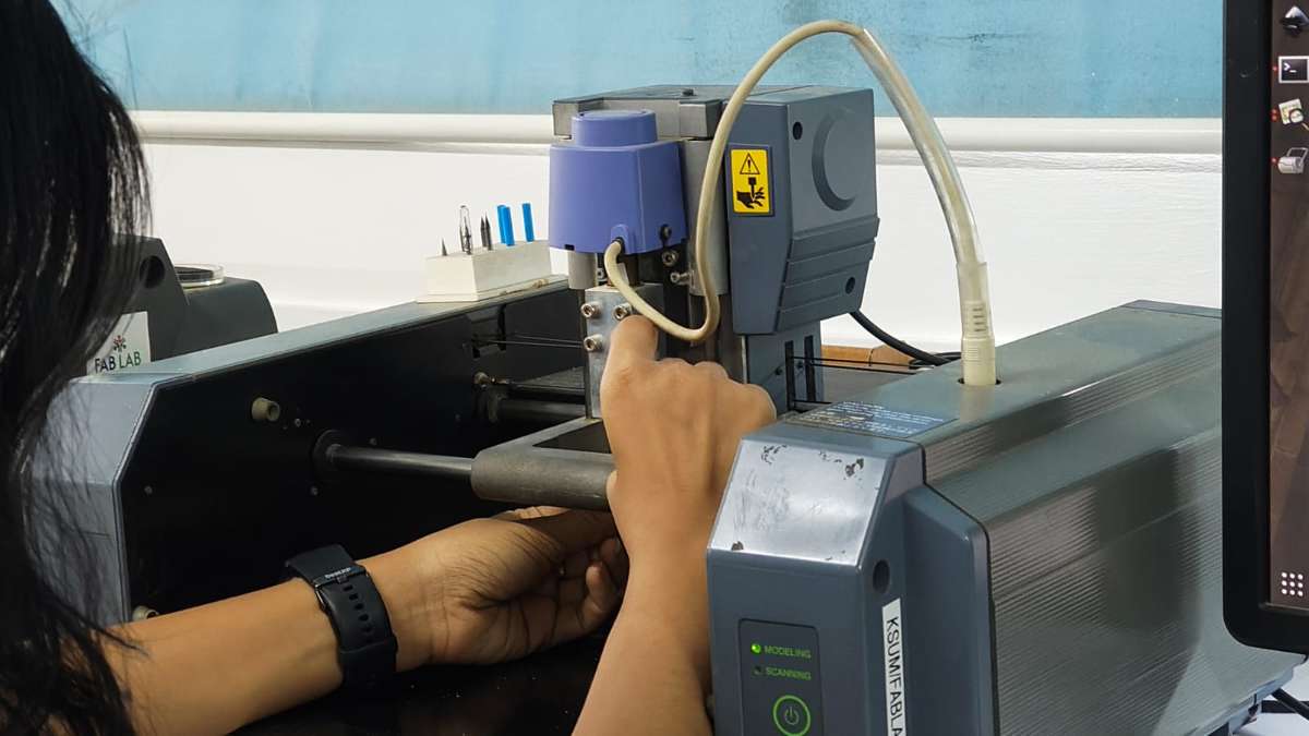 Here, be careful not to push the bit into the machine with force, because then the entire bit will get inside the machine and you and your instructor will have a very hard time taking it out.
 After correctly inserting the bit, you go back to the mods software, and change the bit settings to the one for 1/32 bit and click calculate.
 then send the file to the machine and it will start drilling.
Cutting the PCB outline
After the drilling is complete, we input to the 3rd img, which is the outline part, here, no need to change the settings, click calculate and send file.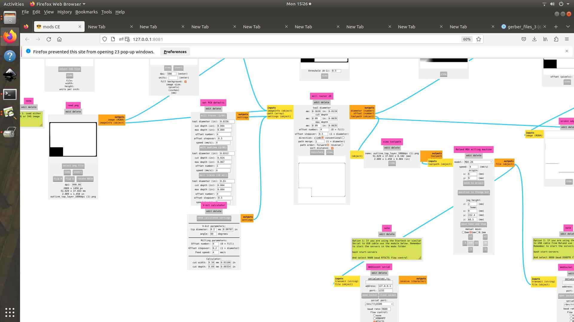 After its done, vacuum the PCB to remove all the material particles.
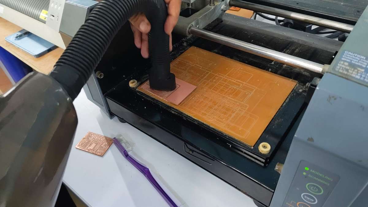
 Next we have to take out the PCB board and sand it.
 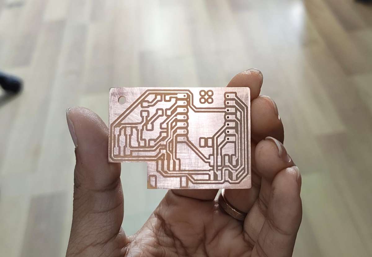 In our Kochi lab we have to request the components we need for our PCB through an inventory called FABSTASH
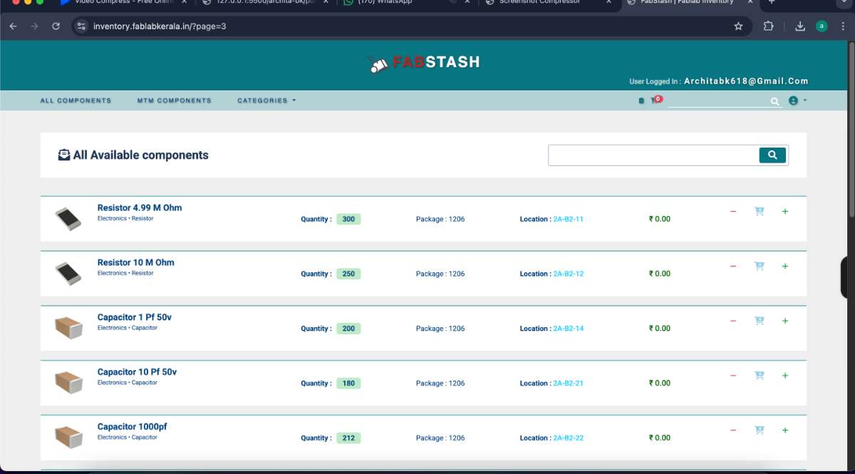 and you select all the components you need and request it to your instructor. Then you can proceed to take components.
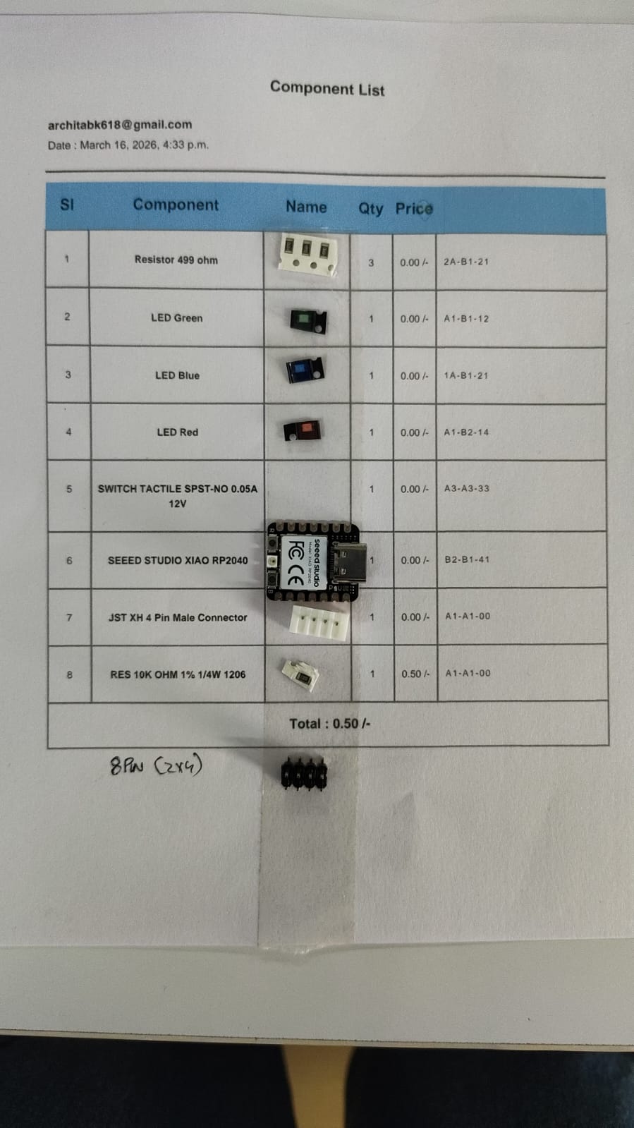 At that time we did not have buttons so i couldn't place it there.
Soldering the PCB
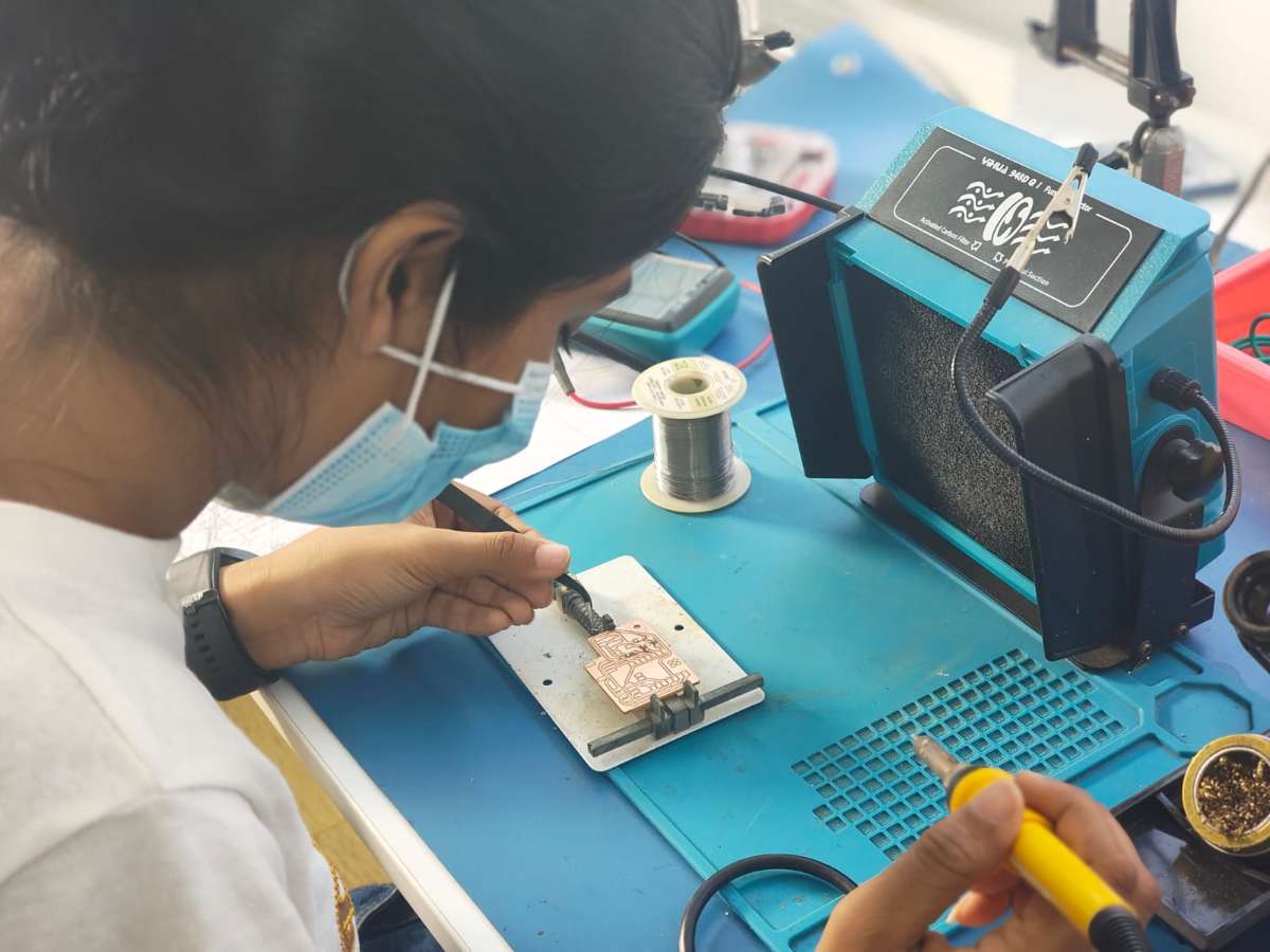
Below image shows the items used for soldering: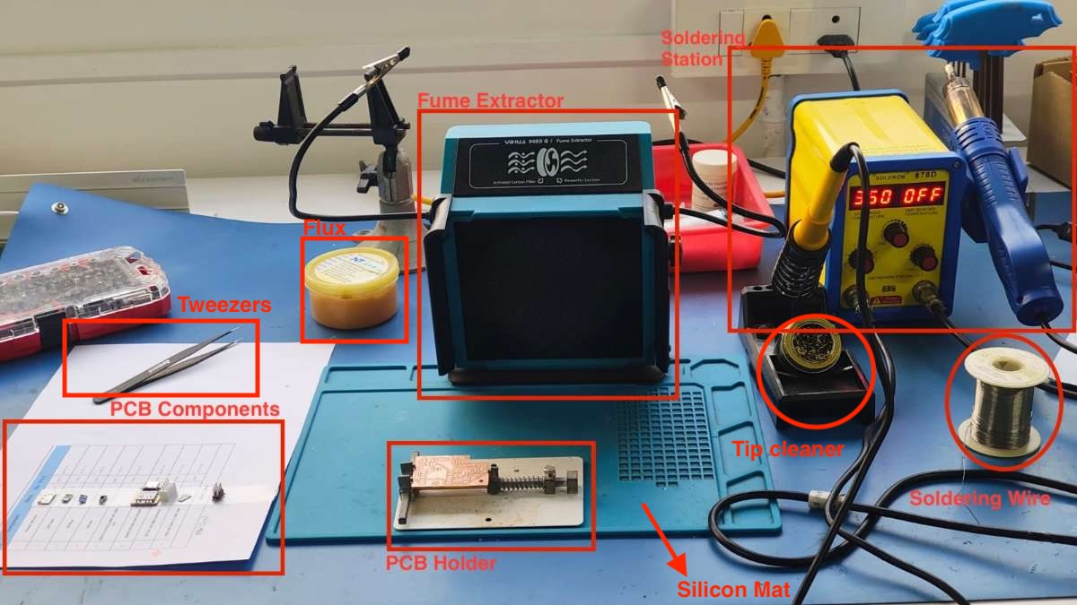 First you place the PCB in place using a PCB holder.
 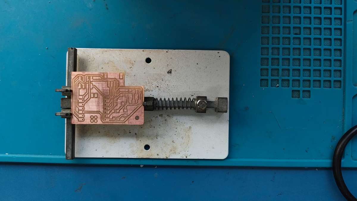 Soldering process Steps:
Heat the soldering iron to proper temperature (~350°C).
Heat the pad(area where component is placed) with the iron tip.
Apply solder wire to the heated pad (not directly to the iron).
Place SMD parts.
Allow solder to flow and form a shiny joint while pressing the component in place.
Remove iron and let it cool naturally (avoid movement).
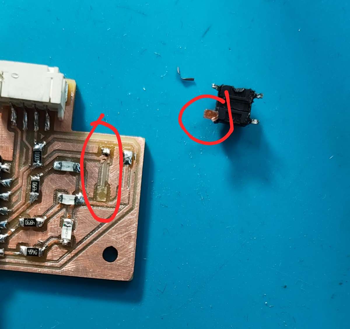
 I managed to pull off the button along with the copper clad, this is why you should use the desoldering pump to remove solder.
 This is how the PCB looked after soldering:
 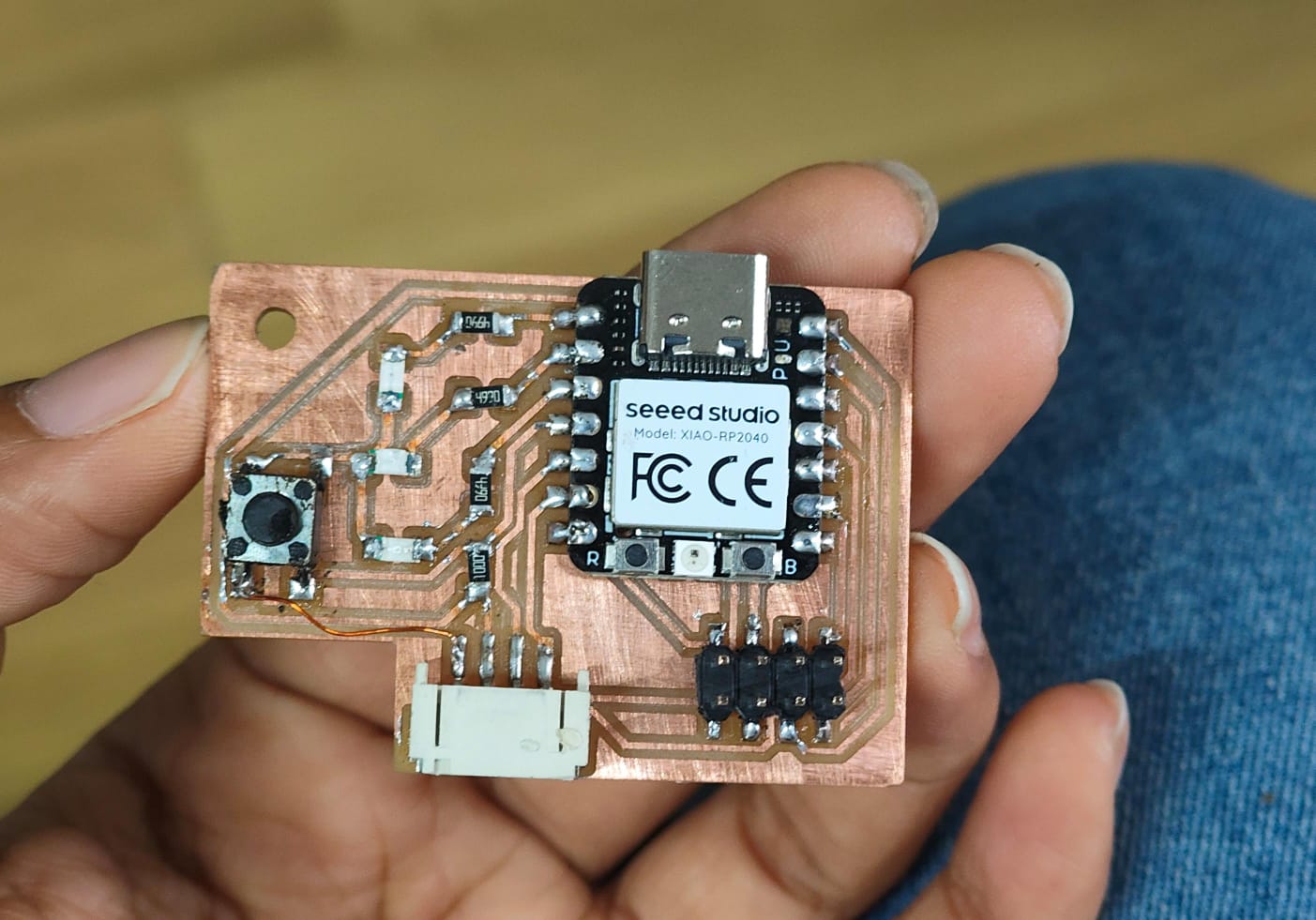 Labelled PCB
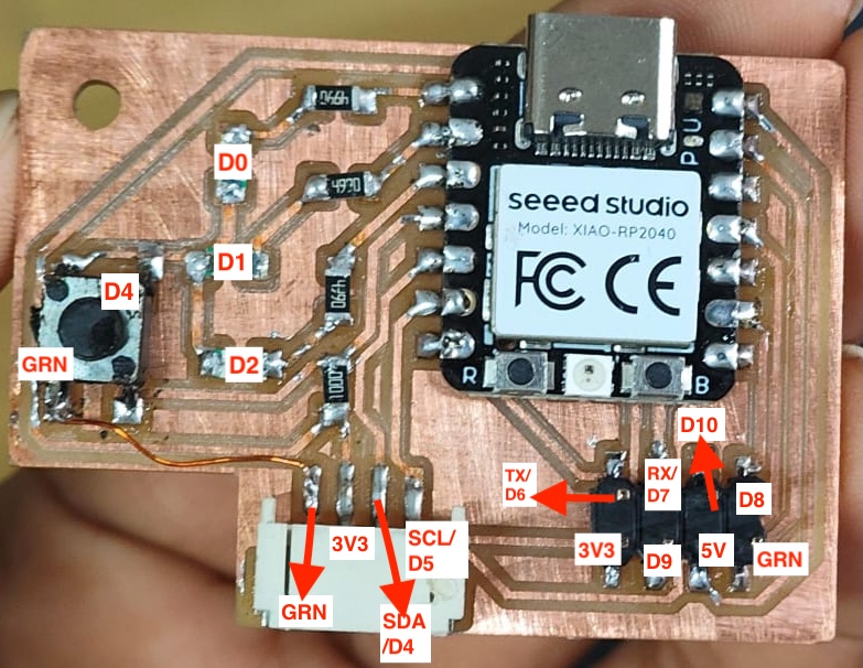
Testing the PCB
Now to see if there are any shorts in the circuit i checked it with USB meter and the multimeter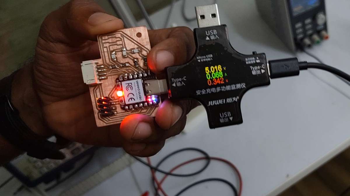 No shorts were shown in the USB meter but while trying out the multimeter i recognized that the ground pins from either
of the sides were not connected and surprisingly enough there were no air wires as well. I have no idea how i missed it out. i had to solder a jumper wire with the help of an instructor, Sibin, to get it right.
No shorts were shown in the USB meter but while trying out the multimeter i recognized that the ground pins from either
of the sides were not connected and surprisingly enough there were no air wires as well. I have no idea how i missed it out. i had to solder a jumper wire with the help of an instructor, Sibin, to get it right.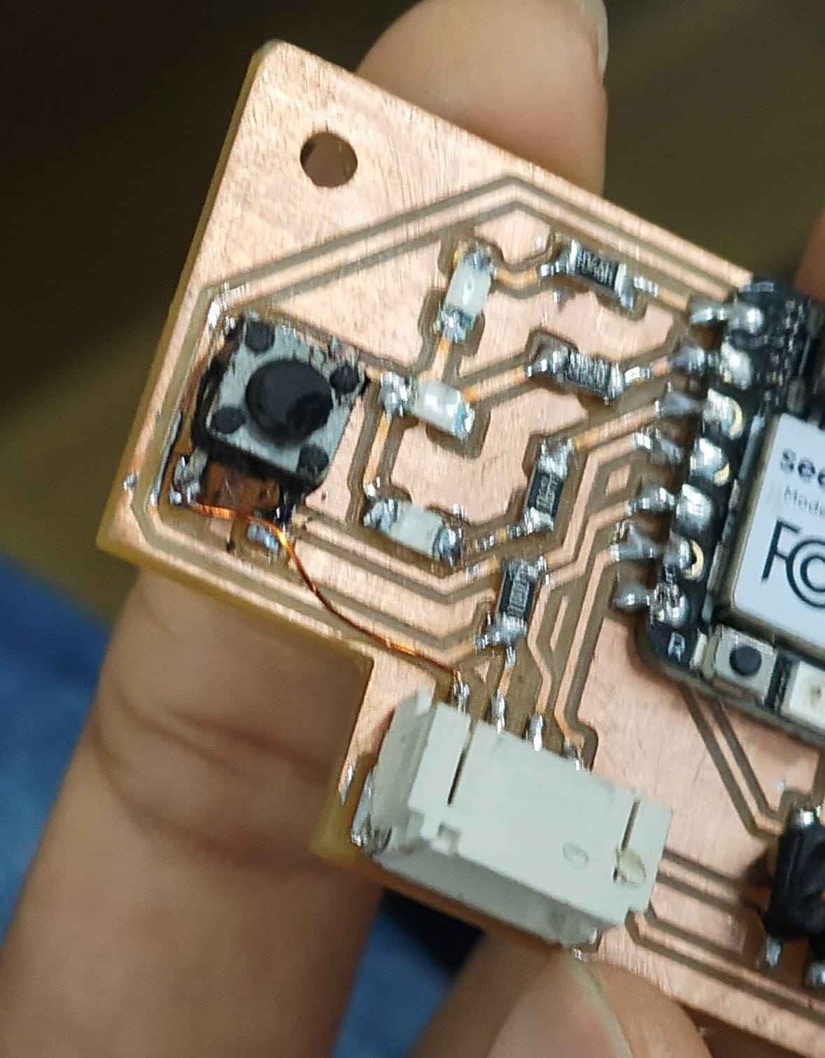 I tested the PCB with my light race program from week6 and it worked.
About XTool
Xtool is a leading brand specializing in desktop laser cutters, engravers (diode, CO2, infrared), and smart fabrication tools for hobbyists and small businesses.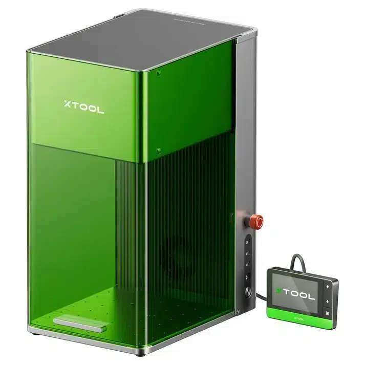
Making PCB using XTool
Here, i have made slight changes in the PCB such as:Trace & spacing
Min trace width : 0.4 mm
Min trace-to-trace spacing : 0.45 mm
Recommended spacing : 0.6 mm
Pads & isolation
Min pad to trace : 0.25 mm
Min via diameter : 0.8mm
Via-to-trace clearance : 0.3 mm
Pad-to-edge margin : 1.0 mm
Then for Laser cutting the PCB i'll generate gerber2png images.
 Next i generated & downloaded the following image so that it will be easier to place as a whole in the Xtool software with the above image
 Then i imported them to Xtool Studio, it is a free, revamped desktop software designed by xTool to operate their laser cutters.
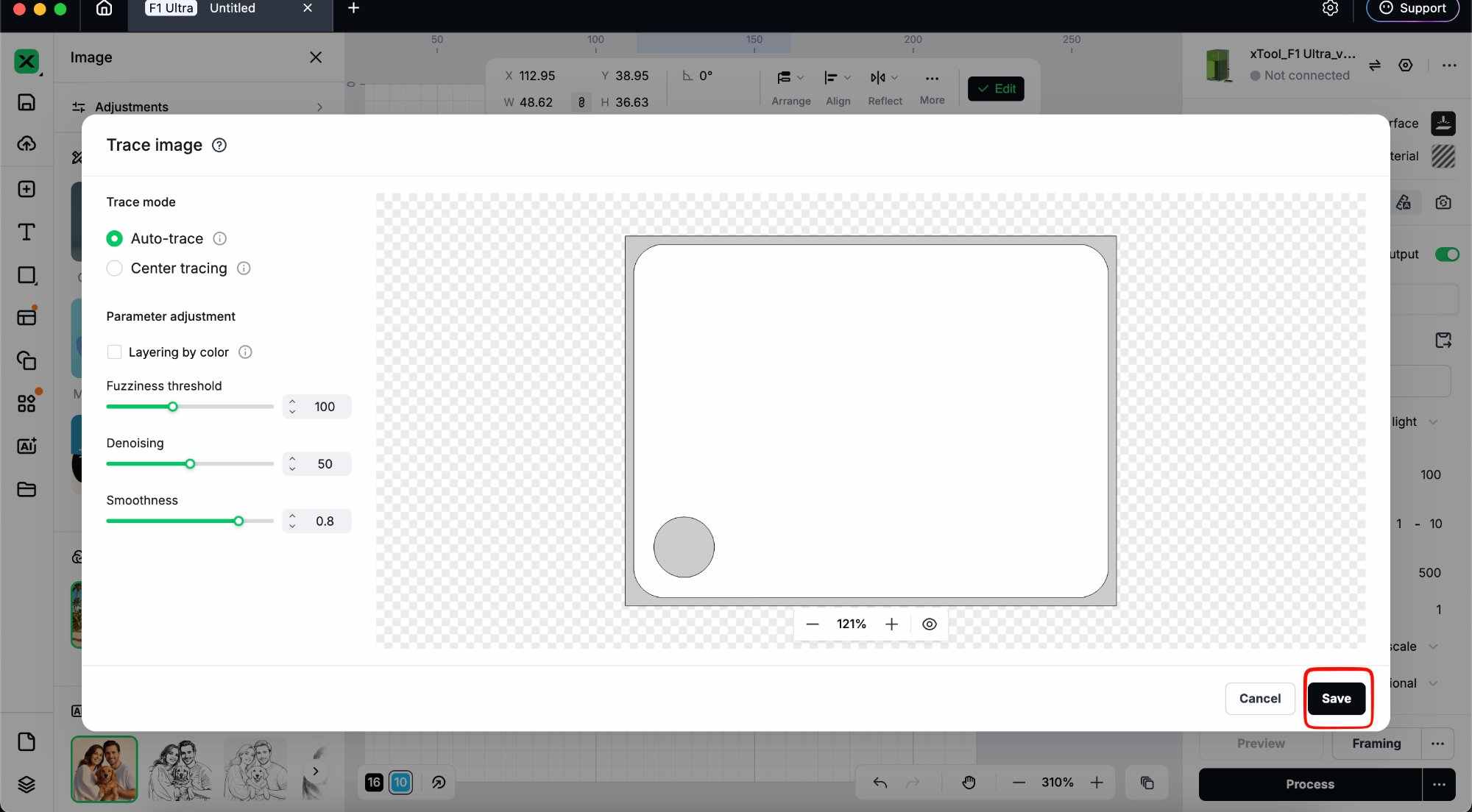
First we trace the image .
Then i imported them to Xtool Studio, it is a free, revamped desktop software designed by xTool to operate their laser cutters.
First we trace the image . 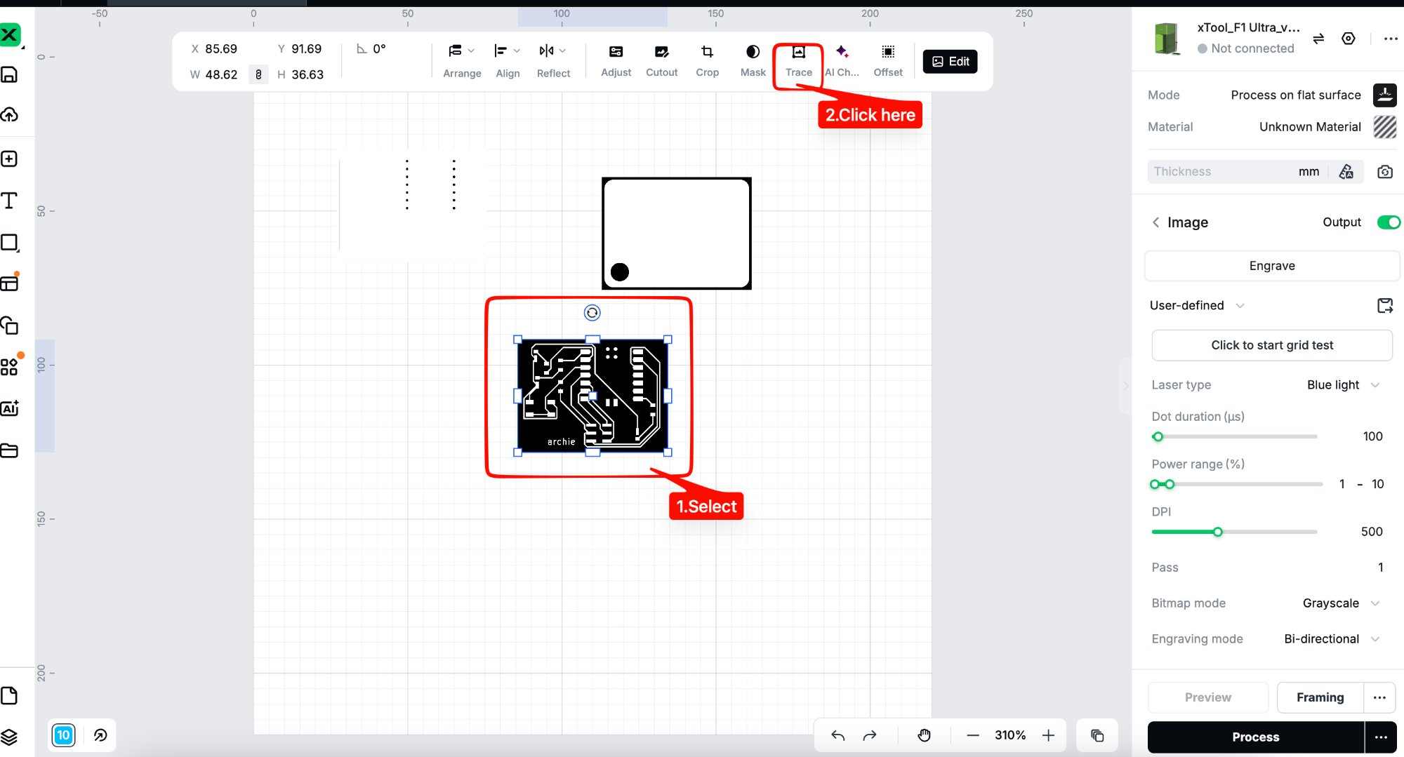 Then this window pops up, and you save the trace
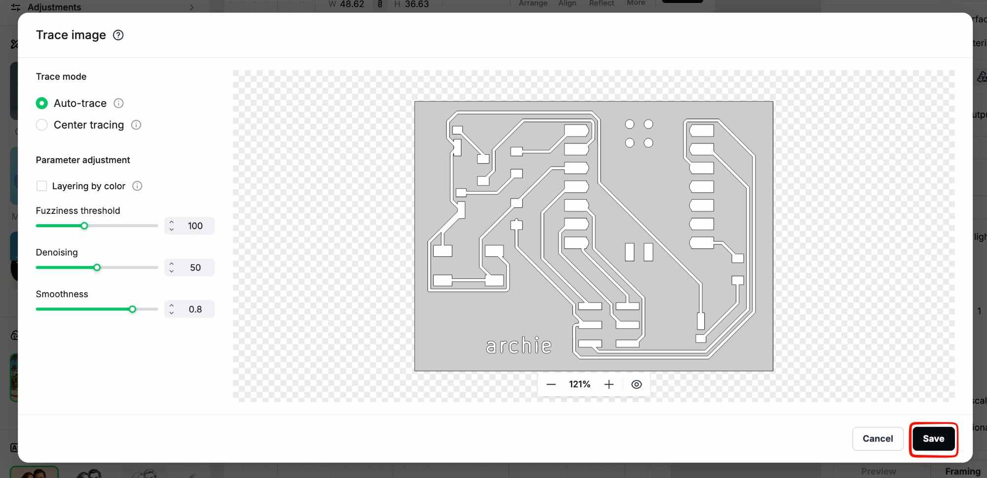 Likewise do it for the other image
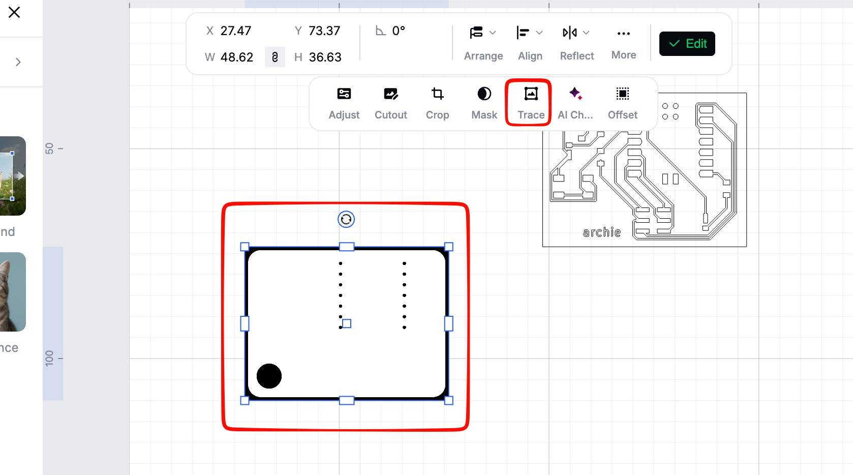
 Then align them together
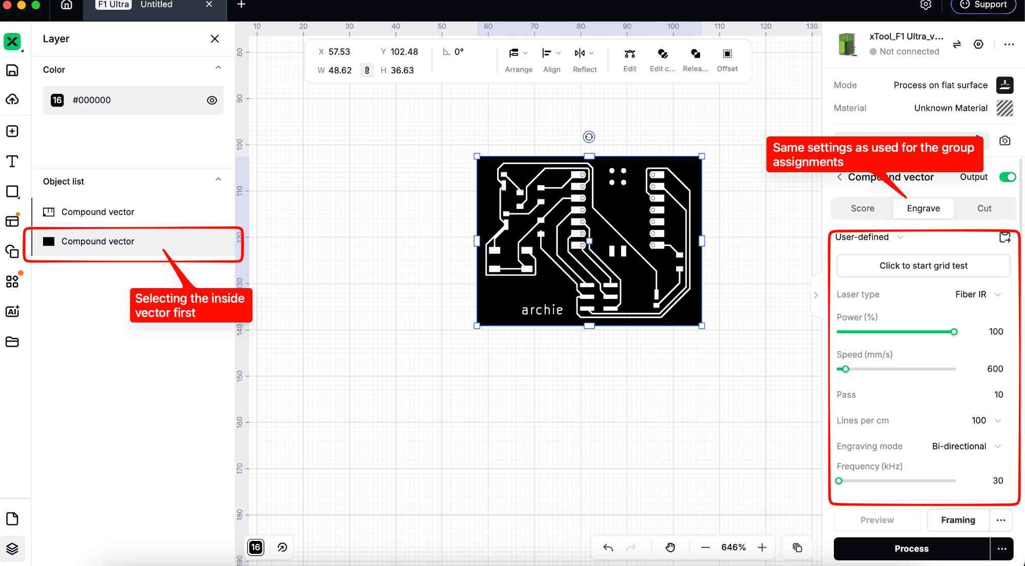
 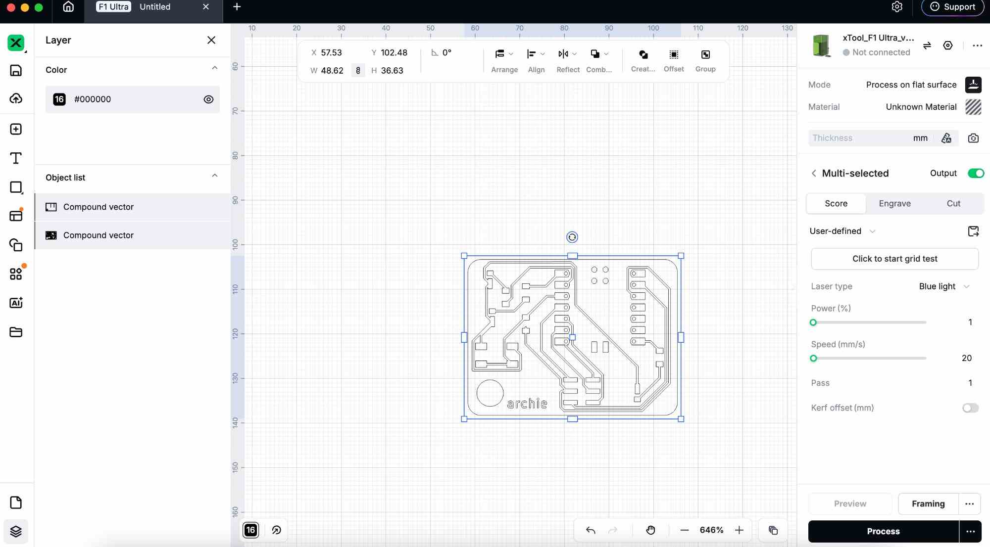 Select the inner vector first and then click engrave, set the settings as shown in the images below:
 Then select frame as we did on the laser cutting week and then click process. Now the engraving process has started.
You will have to do this about 3-5 times to get all the copper out.
Select the outer vector next and then click cut, set the settings as shown in the images below:
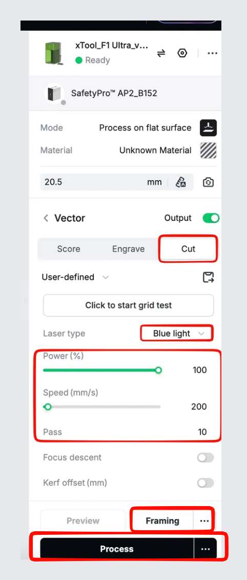
Again, you'll have to repeat the process 2-4 times, you won't bw able to get a perfect cut but the impact of the laser will be enough tho bend and tear away rest of the material.
The following the result:
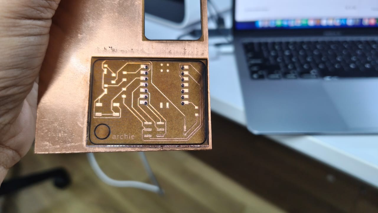 After cleaning and tearing of the rest of the material using a plyer this is how it looked:
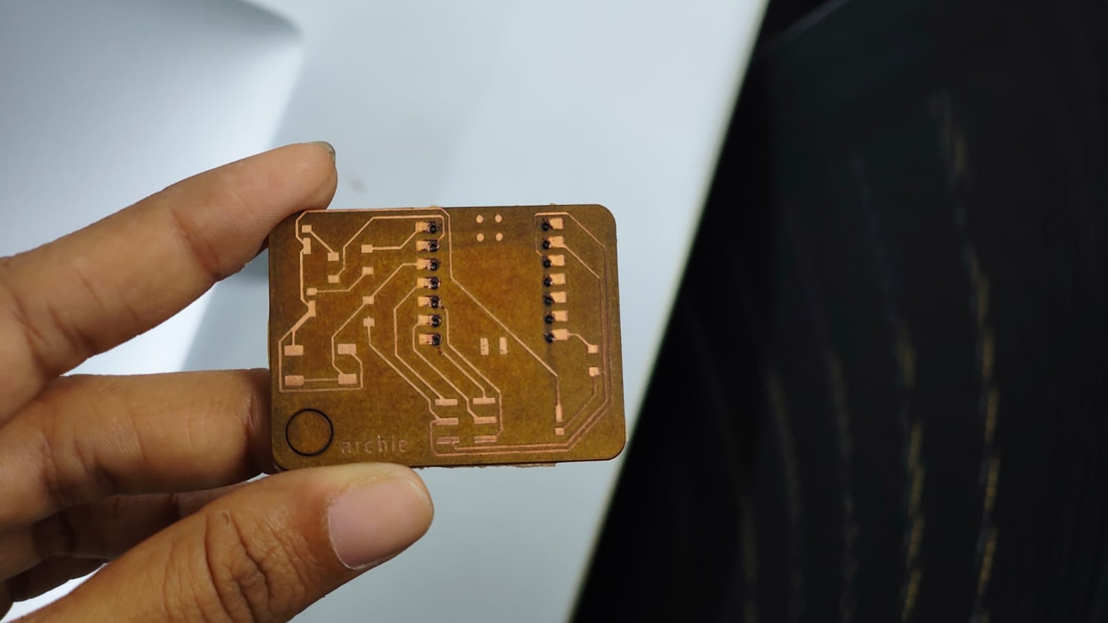 (hero shot)
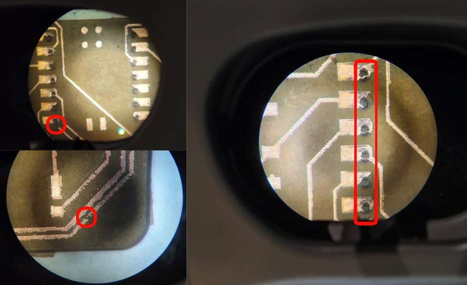
But after inspecting it under the microscope to see whether their was any unwanted removal of copper,i found out that multiple points had broken traces and that all the holes were properly cut & had removed its surrounding deposits
Conclusion
This week felt like a full circle moment. From taking a PCB I had already designed earlier and finally fabricating it. Trying PCB fabrication with the xTool was also a useful experiment, but it showed limitations compared to milling.Overall, this assignment helped me gain more confidence in handling machines and understanding the complete workflow of PCB production.Final Files
Laser Cutting FilesMilling Files
Code File