Week 10 – Output Devices
This week is basically about creating physical output such as light, motion or sound. The output might be based of the input data that we captured during the last week. I may develop a new controller or use the one that I developed during electronic production week.
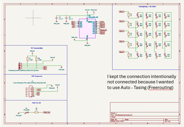
AI prompt ChatGPT: "can you give me my avatar an animated landscape image (I don't want realistic image)- where in I am making Charlieplexing PCB, I milled 2 layer PCB, used fiber optical laser to cut kapton tape then used Kapton tape for 3rd layer. The image should depict the I am doing digital fabrication and Programming/Coding and Testing 5 X 4 LED charlieplexing matix."
Assignment Overview
- Measure the power consumption of an output device
- Add an output device to a microcontroller board you've designed, and program it to do something
| Day | Activity | Status |
|---|---|---|
| Thursday | Class, Group Assignment 📐 and Group Assignment Documentation📝 | Completed |
| Friday | Week Planning 📅, LAB Activity 🛠 and Documentation 📝 | Completed |
| Saturday | Brainstorm for Machine Building week | Completed |
| Sunday | Watch Input Week 📺 | Completed |
| Monday | LAB Activity 🛠 - Charlieplexing PCB Design | Complete |
| Reflection and Learnings 💡 | Completed | |
| Complete Documentation - Regional Review 📝 | Completed | |
| Tuesday | Regional Review 👨🏫💬 | Completed |
| Lab Activity 🛠 - Charlieplexing PCB Milling | Completed | |
| Wednesday | Go the Extra Mile - On Final Project⚙️ | Completed |
| NuEval - Final Documentation 🏁 | Completed |
Group Assignment
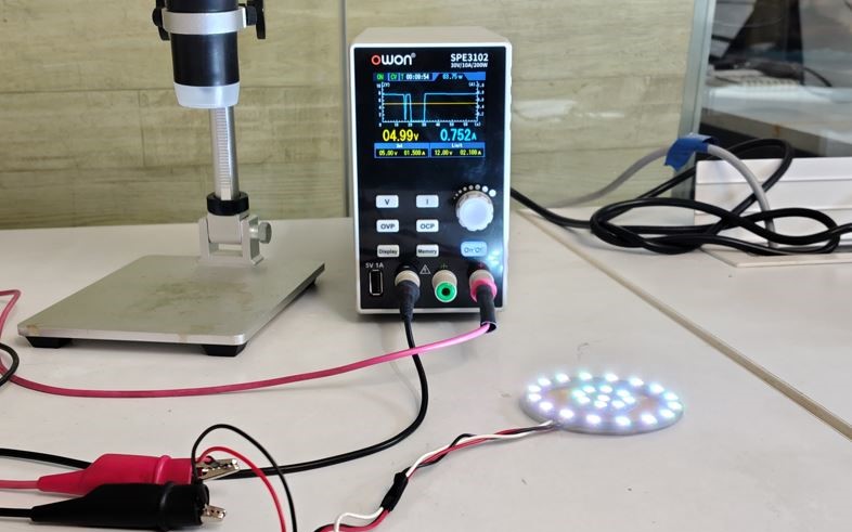
As part of the group assignment, we calculated the power consumption of a Servo motor and Neopixel LEDs using bench power supply. Group Assignment
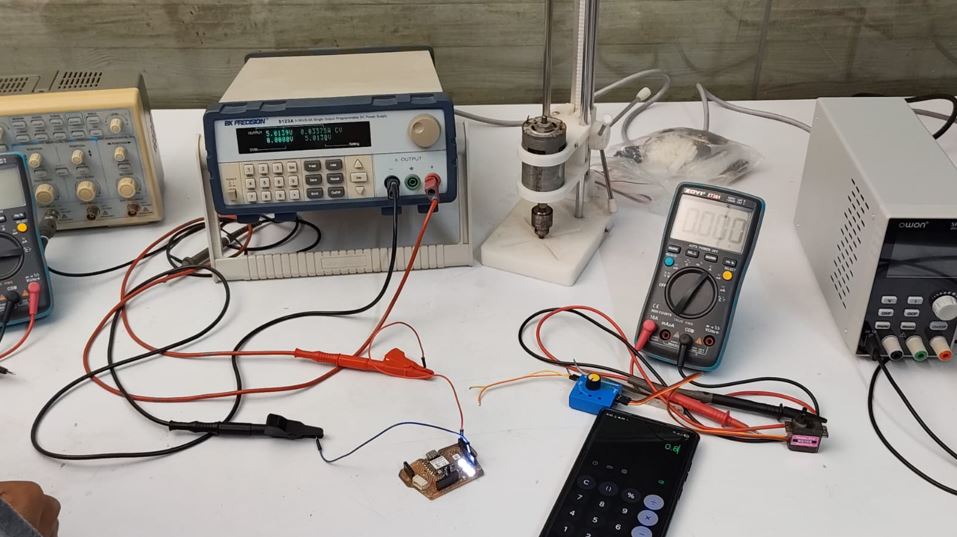
To calculate the power consumed by a device, we measured the supply voltage and current using DC supply or Multimeter and then applied the following formula:
Power (W) = Voltage (V) × Current (A)
For the NeoPixel test setup:
- Supply Voltage: 5 V
- Measured Current: 0.0337 A
Thus, Power = 5 × 0.0337 = 0.1685 W. Therefore, the three NeoPixels consumed approximately 0.17 W of power during the test.
Group Assignment Link
Output Device - Neopixel
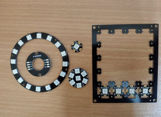
As my project is on integrating Neopixel RGBs with Traditional embroidery work I choose to work with Neopixel WS2818B in my output device week.
These Neopixel are connected in series supply pins and ground pins of all Neopixels are connected and data-out of first is connected to data in of next Neopixel , the first one takes off it's values and passes on the information to next one, the next one takes it off and my message hops through them.
WS2818B is the IC inside the NEOPIXEL 5050. The package 5050 is from Adafruit Industry.
PIN Functions
- Pin 1: VDD power supply
- Pin 2: DOUT Control Data Signal Output
- Pin 3: VSS Ground
- Pin 4: DIN COntrol Data pin signal input
Absolute values
| Parameter | Symbol | Ratings | Unit |
|---|---|---|---|
| Power supply voltage | VDD | +3.5 ~ +5.3 | V |
| Input voltage | VI | -0.5 ~ VDD + 0.5 | V |
| Operation junction temperature | Topt | -25 ~ +80 | °C |
| Storage temperature range | Tstg | -40 ~ +105 | °C |
Microcontroller Board
While designing my week 8 electronic production I added totaL 4 Neopixels one connected to Pin D10 and 3 connected to pin D10. I added them already because I knew that my project involves Neopixels as output device.
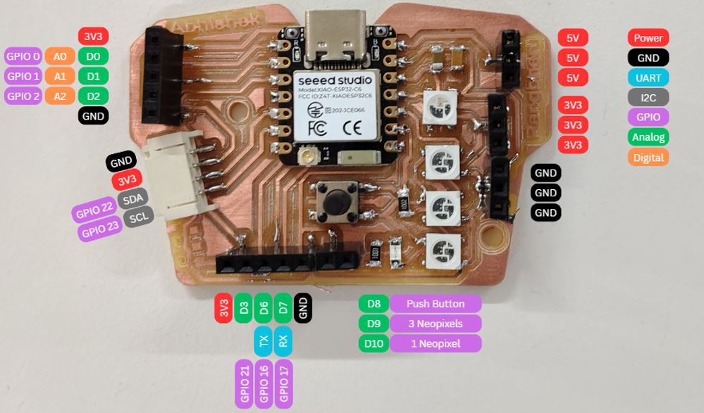
- Pin D9 has 3 Neopixels
- Pin D10 has 1 Neopixel
My Objective in testing Neopixel:
- Understand the Neopixel Protocol
- Single-wire Control, Self-Clocking (no separate clock wire)
- Each Neopixel needs 3 bytes of data (Red, Green, Blue) - Total 24bits
- Thus after transmission for each pixel,the data is reduced 24bit
- Operates at roughly 800kHz (1.25us per bit)
- After the data for the entire strip is sent, the data line is held low for a reset period typically >50µs
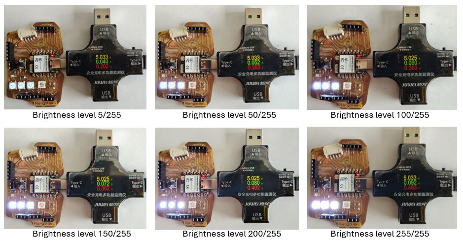
- Power Measurement deciding battery rating
- Brightness Level 005 --> Voltage 5.016V --> Current 0.044A --> Power 0.202W
- Brightness Level 050 --> Voltage 5.033V --> Current 0.052A --> Power 0.263W
- Brightness Level 100 --> Voltage 5.033V --> Current 0.060A --> Power 0.303W
- Brightness Level 150 --> Voltage 5.033V --> Current 0.072A --> Power 0.362W
- Brightness Level 200 --> Voltage 5.025V --> Current 0.080A --> Power 0.402W
- Brightness Level 255 --> Voltage 5.033V --> Current 0.092A --> Power 0.462W
- ESP-32C6 Consumption --> Voltage 5.025V --> Current 0.044A --> Power 0.222W
- Identify the way of portable/battery 5V power supply for LEDs
- Develop program blocks based on Adafruit_NeoPixel.h library for WS2818B.
- Use array for RED, GREEN and BLUE value
To measure power, I planned to turn on 1 Neopixel with White color with different brightness levels.
#define PIN        D9  // Define NeoPixel data line
#define NUMPIXELS  3   // Total no. of NeoPixels at D9
#include   // Include NeoPixel library

// Create an object named 'pixels'
// Parameters:
// 1. Number of LEDs
// 2. Pin used for communication
// 3. LED type + signal speed (GRB order + 800kHz timing)
Adafruit_NeoPixel pixels(NUMPIXELS, PIN, NEO_GRB + NEO_KHZ800);

void setup() {

  pixels.begin();
  // Initialize NeoPixel communication
  // Sets the pin as OUTPUT and prepares internal buffers

  pixels.setBrightness(50);
  // Set overall brightness (0 to 255)
}

void loop() {

  // Loop through each LED (index 0 → 2)
  for (int i = 0; i < NUMPIXELS; i++) {

    pixels.setPixelColor(i, pixels.Color(255, 255, 255));
    // Set color of LED at position 'i'
    // pixels.Color(R, G, B)
    // (255,255,255) = White (full intensity of all colors)
  }

  pixels.show();
  // VERY IMPORTANT:
  // Sends all color data to LEDs
  // Without this → LEDs will NOT update
}
Brightness level range : 0 to 255
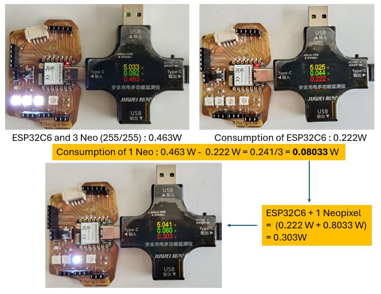
To confirm above, I tested array of 25 neopixels according to above calculation it shall consume about 2.23 W [(0.222) + (25 X 0.0833)], however the results I got is 3.73W (5V X 0.746A). Next I need to measure power consumption of XIAO ESP32S3.
A few of the important commands to control Neopixel array are as below.
First thing first we need to create object name for example 'pixels'
pixels.begin() : Initialize communication with the LED strip
pixels.setBrigthness() : if defined in setup - sets global brightness level (0 to 255), But if defined in loop, we can change the brightness level based on different parameter such as heart-beat, mood, or battery voltage level (0 to 255), keeping level 50 helps reduce power consumption and glare.
pixels.Color(R, G, B) : by changing the RGB values we get different colors.
pixels.clear() : Sets all LEDs’ color values to (0, 0, 0), Which means BLACK = OFF, sets all LEDs to OFF in memory
pixels.show() : VERY IMPORTANT LINE, Sends all stored color data to the LED strip, Without this → LEDs will NOT update, we write instructions quietly… and only when you say show() they perform.
pixels.setPixelColor(i, pixels.Color(255, 0, 0)) : Set LED at index 'i' to a specific color, in this case red.
Program Credit note: I used above command to make and update the below code to get different blinking patent of the Neopixels in the subsequent programs below.
  #include <Adafruit_NeoPixel.h>
  // Include the NeoPixel library
  // This library handles communication with WS2812 / NeoPixel LEDs

  #define PIN D9
  // Define which pin is used to send data to the LED strip
  // D9 is the data line connected to NeoPixels


  #define NUMPIXELS 25
  // Total number of LEDs connected in the strip


  // Create an object named 'pixels'
  // This object controls all LEDs
  Adafruit_NeoPixel pixels(NUMPIXELS, PIN, NEO_GRB + NEO_KHZ800);

  // Parameters explained:
  // NUMPIXELS → total LEDs
  // PIN → data pin
  // NEO_GRB → color order (Green, Red, Blue)
  // NEO_KHZ800 → communication speed (800 kHz, standard for WS2812)


  void setup() {

    pixels.begin();
    // Initialize communication with the LED strip
    // Internally:
    // Sets PIN as OUTPUT
    // Prepares memory buffer for LED data


    pixels.setBrightness(50);
    // Set global brightness level (0 to 255)
    // 50 ≈ dim (~20% brightness)
    // Helps reduce power consumption and glare
  }


  void loop() {

    // Loop through each LED from 0 to 24
    for (int i = 0; i < NUMPIXELS; i++) {

      pixels.setPixelColor(i, pixels.Color(50, 50, 50));

      // Set LED at index 'i' to a specific color

      // pixels.Color(R, G, B):
      // 255 = full intensity
      // 0   = off

      // (255, 0, 0) → RED
      // (0, 255, 0) → GREEN
      // (0, 0, 255) → BLUE
      // (255,255,255) → WHITE
    }

    pixels.show();
    // VERY IMPORTANT LINE

    // Sends all stored color data to the LED strip
    // Without this → LEDs will NOT update

  }
  #include <Adafruit_NeoPixel.h>
  // Include the NeoPixel library

  #define PIN D9
  // Define which pin is used to send data to the LED strip

  #define NUMPIXELS 25
  // Total number of LEDs connected in the strip


  // Create an object named 'pixels'
  // This object controls all LEDs
  Adafruit_NeoPixel pixels(NUMPIXELS, PIN, NEO_GRB + NEO_KHZ800);

  // Parameters explained:
  // NUMPIXELS → total LEDs
  // PIN → data pin
  // NEO_GRB → color order (Green, Red, Blue)
  // NEO_KHZ800 → communication speed (800 kHz, standard for WS2812)


  void setup() {

    pixels.begin();
    // Initialize communication with the LED strip
    // Internally:
    // Sets PIN as OUTPUT
    // Prepares memory buffer for LED data

    pixels.setBrightness(255);
    // Set global brightness level (0 to 255)
    // 50 ≈ dim (~20% brightness)
    // Helps reduce power consumption and glare
  }


  void loop() {

    // Loop through each LED from 0 to 24
    for (int i = 0; i < NUMPIXELS; i++) {
    pixels.clear();                       // turn all OFF
    pixels.setPixelColor(i, 50, 0, 0);   // turn ONE LED ON
    pixels.show();
    delay(100);
    }

  }
What Went Wrong
I soldered the inner neopixel ring in reverse direction thus as we see in the above video the looping on inner neopixel ring is happening in counter-clockwise direction. To make it clockwise to have similarity with larger outer ring, I need to resolder it. Otherwise the running the "for" or "while loops" will not look harmonious on the both rings.
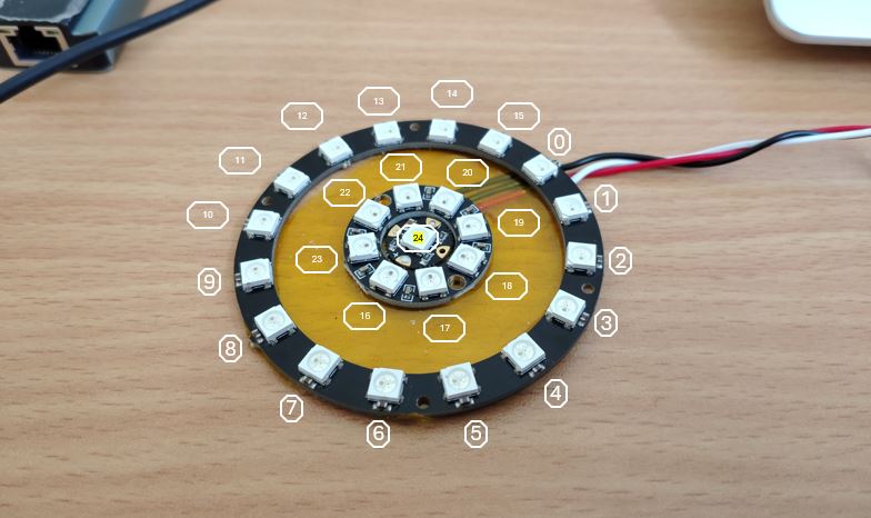
What I Learned
Make sure that when I do molding and casting of "Neopixels - Core", I need to imaging the mirror connection of neopixels - to get clock-wise array direction.
Thus the connection from back side shall be Neopixel 0 at 12 o-clock and then go anti-clockwise until Neopixel 15, then go to inner circle and Neopixel 16 at 12 o-clock and go anti-clockwise until Neopixel 23, and Neopixel 24 at the center.
Thus, the data line connection will need jumper at 15_Out --> 16_In and 23_Out --> 24_In.
And also bring the connection of 24_Out of the molding. This can be helpful in connecting more Neopixels if we run short of GPIO pins.
  #include <Adafruit_NeoPixel.h>
  // Include the NeoPixel library

  #define PIN D9
  // Define which pin is used to send data to the LED strip

  #define NUMPIXELS 25
  // Total number of LEDs connected in the strip


  // Create an object named 'pixels'
  // This object controls all LEDs
  Adafruit_NeoPixel pixels(NUMPIXELS, PIN, NEO_GRB + NEO_KHZ800);

  // Parameters explained:
  // NUMPIXELS → total LEDs
  // PIN → data pin
  // NEO_GRB → color order (Green, Red, Blue)
  // NEO_KHZ800 → communication speed (800 kHz, standard for WS2812)


  void setup() {

    pixels.begin();
    // Initialize communication with the LED strip
    // Internally:
    // Sets PIN as OUTPUT
    // Prepares memory buffer for LED data

    pixels.setBrightness(255);
    // Set global brightness level (0 to 255)
    // 50 ≈ dim (~20% brightness)
    // Helps reduce power consumption and glare
  }


  void loop() {

    // Loop through each LED from 0 to 4
    for (int i = 0; i < 5; i++) {
    pixels.clear();                       // turn all OFF
    pixels.setPixelColor(i, 255, 0, 0);   // turn ONE LED ON
    pixels.setPixelColor(i+5, 255, 0, 0);   // turn ONE LED ON
    pixels.setPixelColor(i+10, 255, 0, 0);   // turn ONE LED ON
    pixels.setPixelColor(i+15, 255, 0, 0);   // turn ONE LED ON
    pixels.setPixelColor(i+20, 255, 0, 0);   // turn ONE LED ON
    pixels.show();
    delay(100);
  }

  }
  #include <Adafruit_NeoPixel.h>
  // Include the NeoPixel library

  #define PIN D9
  // Define which pin is used to send data to the LED strip

  #define NUMPIXELS 25
  // Total number of LEDs connected in the strip


  // Create an object named 'pixels'
  // This object controls all LEDs
  Adafruit_NeoPixel pixels(NUMPIXELS, PIN, NEO_GRB + NEO_KHZ800);

  // Parameters explained:
  // NUMPIXELS → total LEDs
  // PIN → data pin
  // NEO_GRB → color order (Green, Red, Blue)
  // NEO_KHZ800 → communication speed (800 kHz, standard for WS2812)


  void setup() {

    pixels.begin();
    // Initialize communication with the LED strip
    // Internally:
    // Sets PIN as OUTPUT
    // Prepares memory buffer for LED data

    pixels.setBrightness(255);
    // Set global brightness level (0 to 255)
    // 50 ≈ dim (~20% brightness)
    // Helps reduce power consumption and glare
  }


  void loop() {

    pixels.setPixelColor(24, 255, 0, 0);   // turn ONE LED ON
    pixels.show();

    for (int i = 23; i > 15; i--) {
    pixels.setPixelColor(i, 255, 0, 0); }  // turn ONE LED ON
    pixels.show();
    delay(50);
    for (int i = 23; i > 15; i--) {
    pixels.setPixelColor(i, 0, 0, 0); }  // turn ONE LED ON
    pixels.show();


    for (int i = 15; i > -1; i--) {
    pixels.setPixelColor(i, 255, 0, 0); }  // turn ONE LED ON
    pixels.show();
    delay(50);
    for (int i = 15; i > -1; i--) {
    pixels.setPixelColor(i, 0, 0, 0); }  // turn ONE LED ON
    pixels.show();


    delay(700);

  }
What I Learned
pixels.clear() turn-off every Neopixels because it clears internal buffer. There’s no option to pass an index or range. we need to do it manually, pixel by pixel or by using for loop.
Run the loop for with pixels.setPixelColor ( i, 0, 0, 0 ); and then execute Pixels.show() --> this will run the for loop and then turn off all the looped neopixels at once.
pixels.show (); // apply changes
Output Device - Charlieplexing
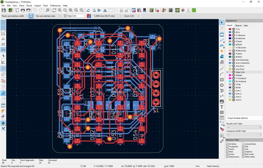
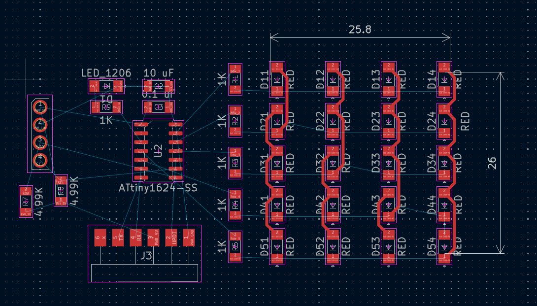
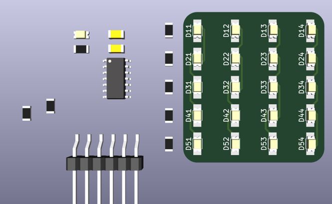
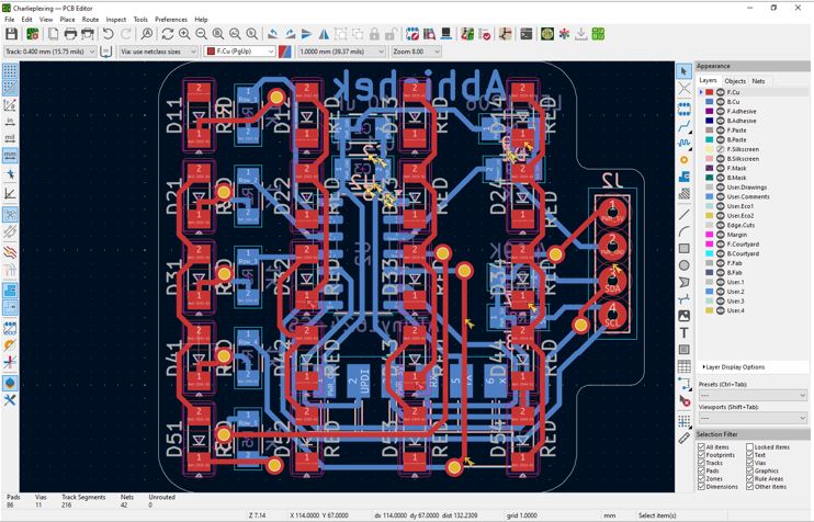
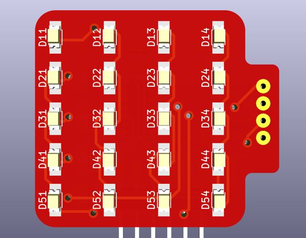
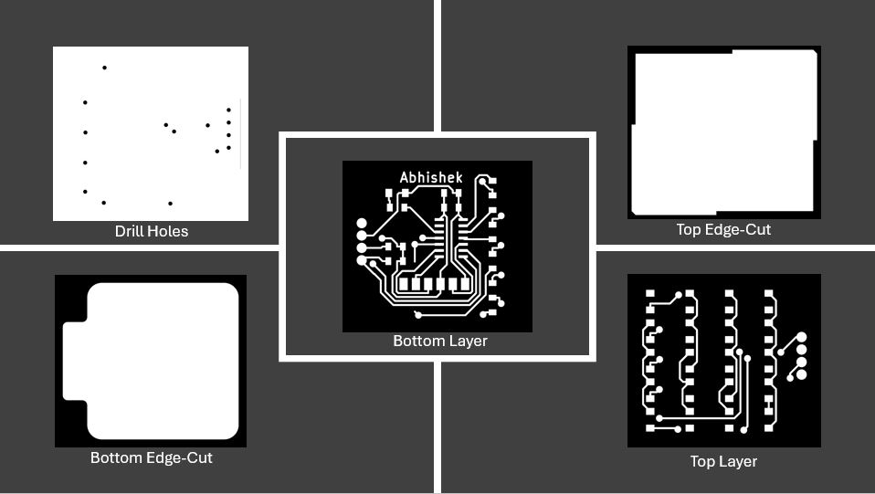
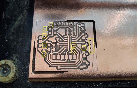
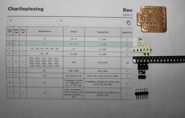
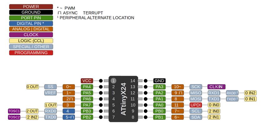
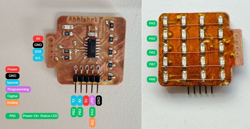
I designed a microcontroller board using ATTiny 1624 and LED Matrix of 5 Rows and 4 Columns as (n) x (n-1). The Charlieplexing concept states that I can control (n) x (n-1) LEDs using n pines of a micro-controller. Thus, here I can control 20 leds using 5 pins of micro-controller ATTiny 1624 IC.
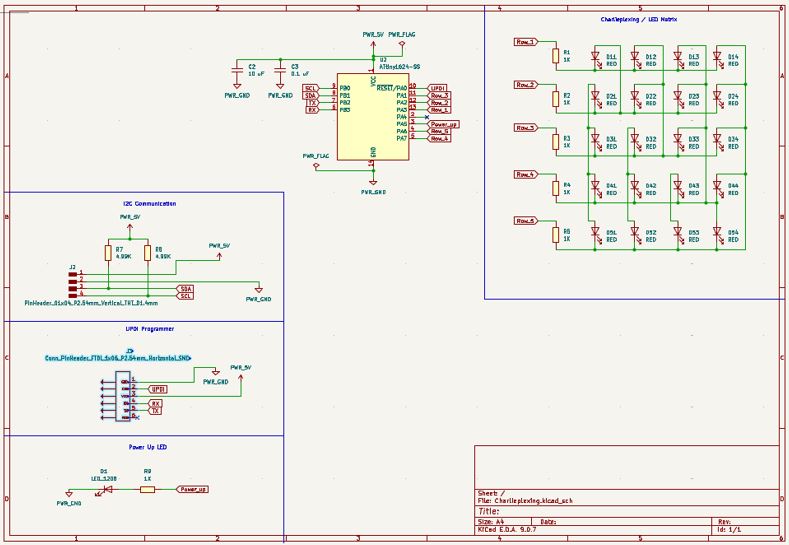
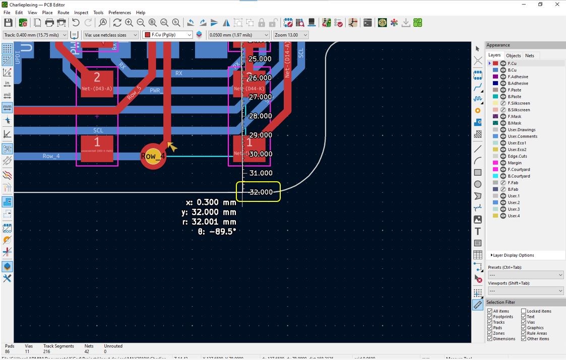
As I wanted to embed the PCB into clothing, I wanted to make the matrix with in 30mm x 30mm area the so I need to go for double layer PCB.
Because of time constrain and under pressure, I chose to use Autoroute tool to trace the paths, however the DRC gave about 344 errors of Trace width and and Trace spacing and made the circuit very complex.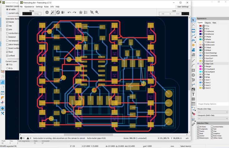
What Went Wrong
Because of time constrain and under pressure, I chose to use Autoroute tool to trace the paths, however the DRC gave about 344 errors of Trace width and and Trace spacing and made the circuit very complex.
What I Learned
My instructor advice me to do manual routing, even though it takes time. Then I figure out optimal way of doing manual and auto routing.
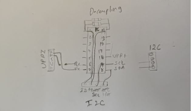
- First, draw a pencil sketch of micro-controller PIN layout and optimally arrange de-coupling capacitors, pull-up resistors, TX/RX straight connection, SDA and SPI lines, Power and GND lines.
- Second, I arranged the components I placed the LEDs at proper equal distance to have symmetric placing and then connected columns and planned to connect row on the Kapton take 3 layers
- Third, I flipped the properly arranged components and moved within the edge-cut layer boundary.
- Forth, after completing above 60-70 % traces manually, and leave the traces that can not be routed, then perform autorouting. The unroute traces will be connected by vias by freerouting tool.
- Fifth, check the positions of Vias and very nearer traces, and rearrange them.
- Last, do the DRC - design rule check.
As this was the complex circuit, I got feedback in the regional review of making 3-Layer PCB, making third layer of connections on Kapton Tape. This I remover the connection that I wanted on Kapton tape from the PCB schematics, so that the Freerouter do not route them and I can connect them later.
First, draw a pencil sketch of micro-controller PIN layout and optimally arrange de-coupling capacitors, pull-up resistors, TX/RX straight connection, SDA and SPI lines, Power and GND lines.
Second, I arranged the components, I placed the LEDs at proper equal distance to have symmetric placing and then connected columns and planned to connect row on the Kapton take 3 layers.
Third, I flipped the properly arranged components and moved within the edge-cut layer boundary.
Forth, after completing above 60-70 % traces manually, and leave the traces that can not be routed, then perform autorouting. The unroute traces will be connected by vias by freerouting tool.
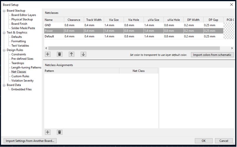
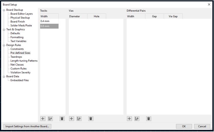
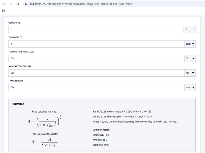
Power/3V3/5V lines and Ground lines trace thickness setup can be done as shown in following images. in Board Setup >> Design Rules >> Constrains >> Add Netclass give them name Power and GND. After that Click >> Pre-defined Sizes >> Tracks width >> add 0.8 mm . This will appear in the dropdown list of traces on the left corner of PCB design window.
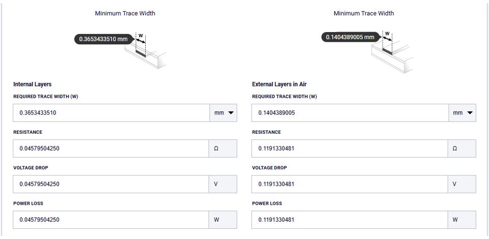
PCB Trace Width Calculator can be use to calculate the trace width based on our current requirement. For example, below I entered current 1A, PCB copper cladding value 1 oz/ft-sq, Temp rise 35 °C, and Ambient Temp 28 °C.
Fifth, check the positions of Vias and very nearer traces, and rearrange them.
Last, do the DRC - design rule check.
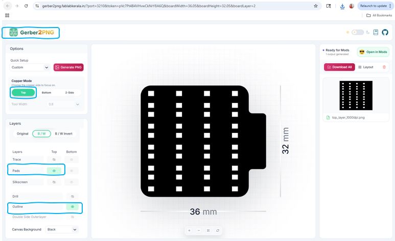
Then I generated PNG file generation using Gerber-to-PNG KiCAD pluggin tool.
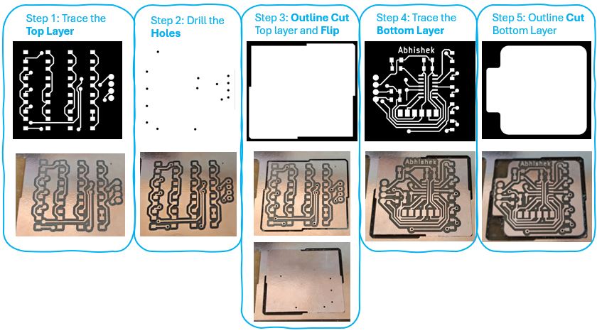
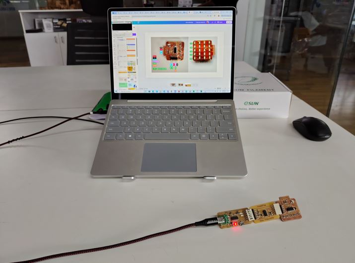
Double-Layer PCB Milling
I first time tried the double layer PCB milling in my fab academy journey.
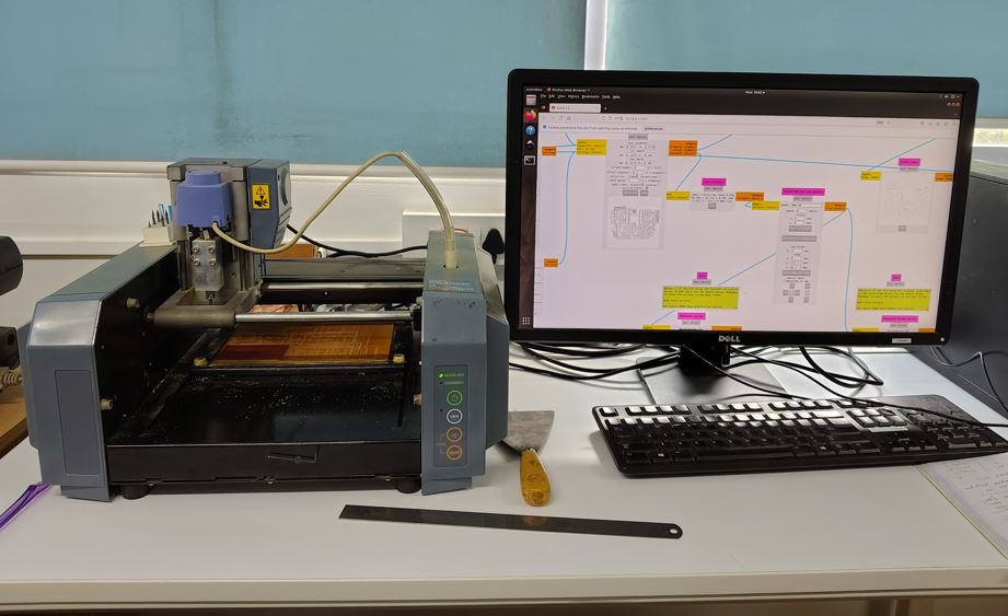
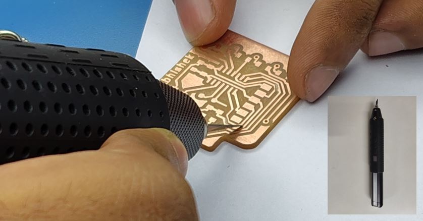
Note : Many times, we see joint traces after PCB milling, wec an use Ultrasonic Cutting Tool to easily dis-joint the traces. By using normal cutter we may end-up cutting other trace lines. Thus always use Ultrasonic Cutting Tool.
What Went Wrong in Double-Layer PCB Milling
At the step-3 after top layer outline cute, I flipped in the wrong direction and thus the via-holes for top layer and trace of bottom layer was not matching after step 4, which is bottom layer tracing.
What I Learned in Double-Layer PCB Milling
Always double check the alignment of vias and bottom layer traces of before starting the Trace Bottom layer operation. I milled the PCB again.
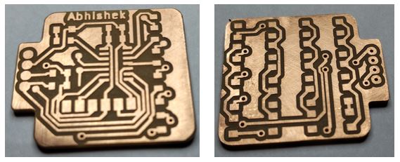
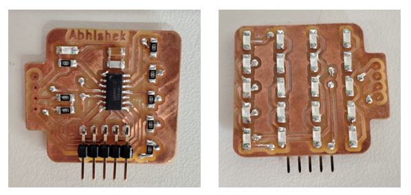
3-Layer PCB Fabrication
The Steps I followed are:
- First, solder the via-holes.
- Second, solder the top LED-Matrix layer.
- Third, solder the bottom layer starting with ATtiny first and then other components.
- Forth, leaser cut the Kapton Tape.
- Fifth, placed the kapton tape and soldered the third layer.
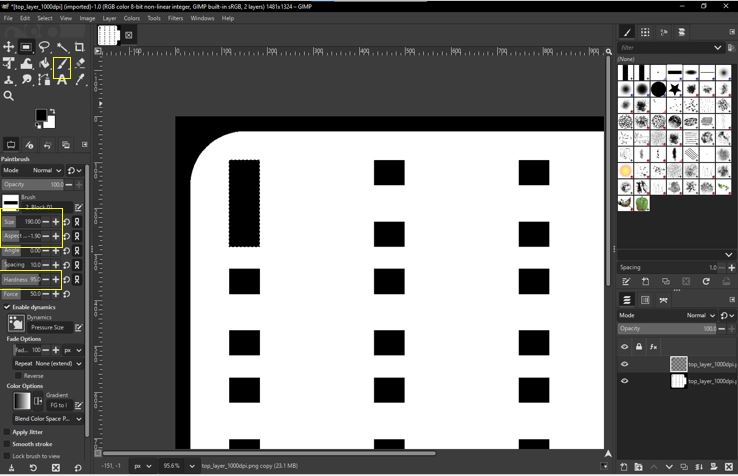
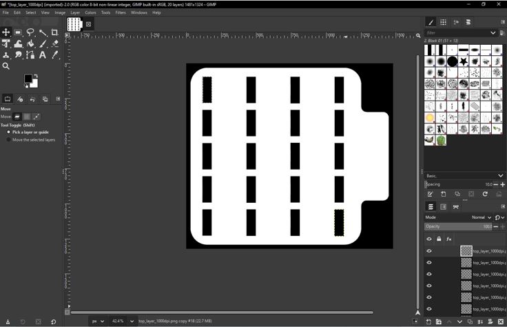
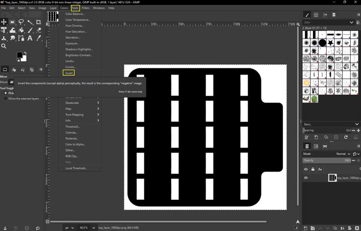
Then, I downloaded the top trace layer PNG without traces it included only pads and outline. and Then I used Gimp to edit the PNG.
I used Gimp , I selected the Brush and then adjusted it's size, aspect-ratio, and hardness. and then drew the black pads (basically connecting the LED pads vertically to have LED cutout).
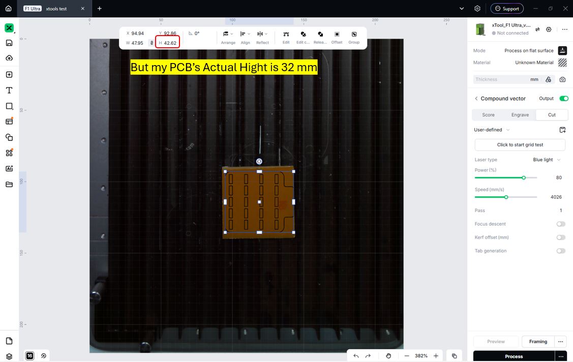
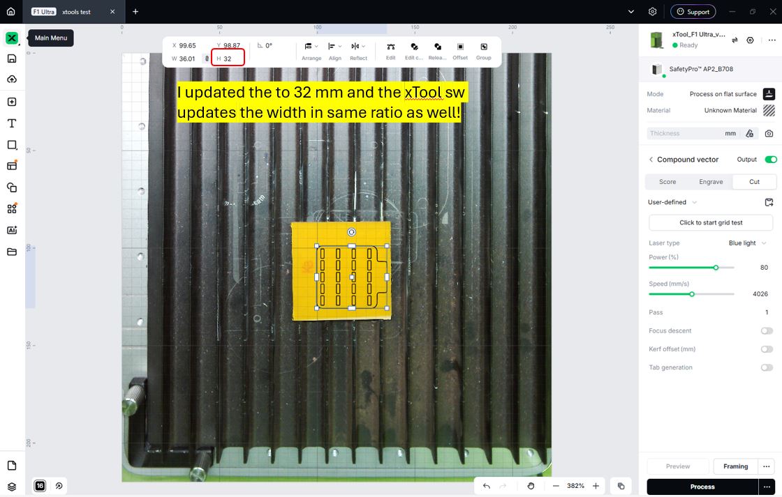
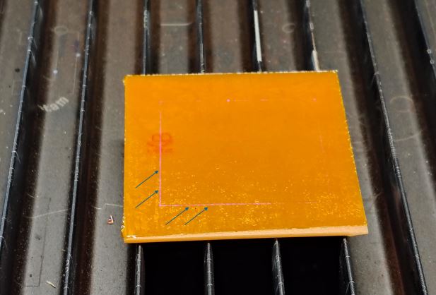
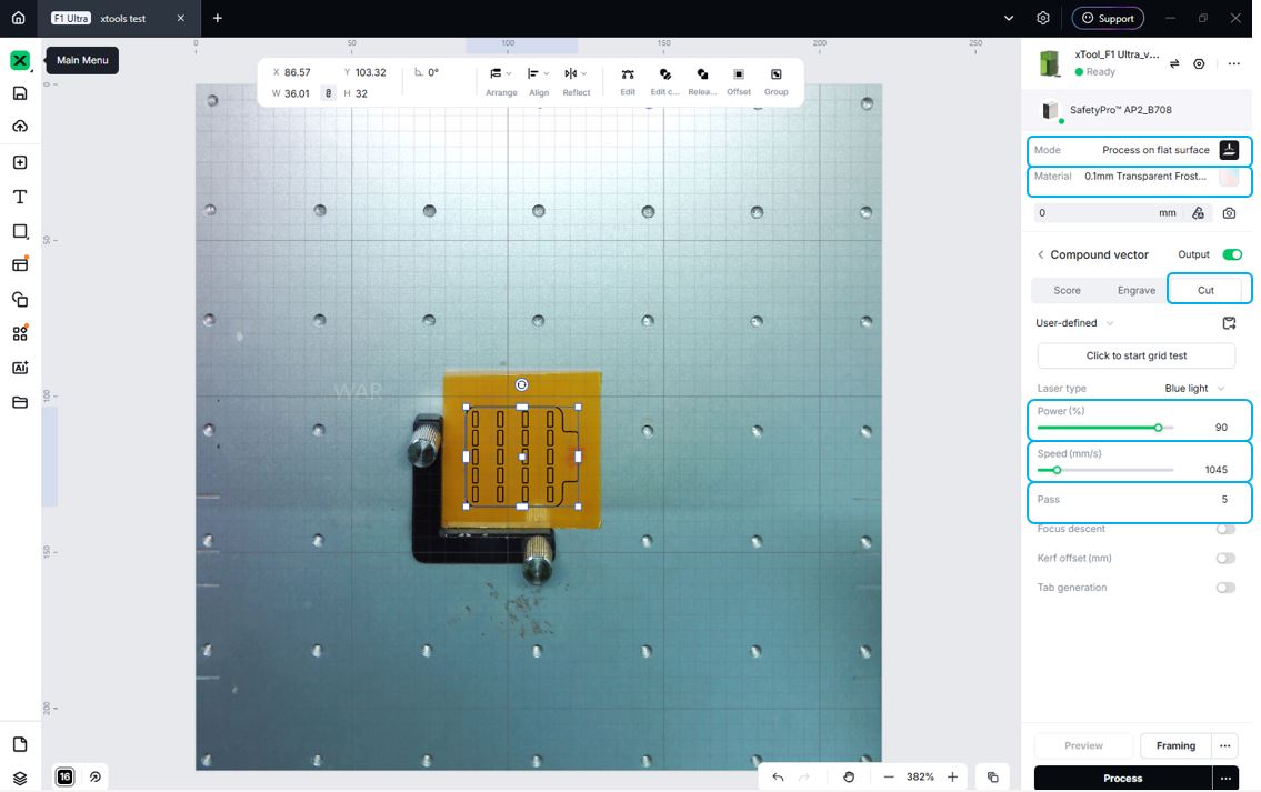
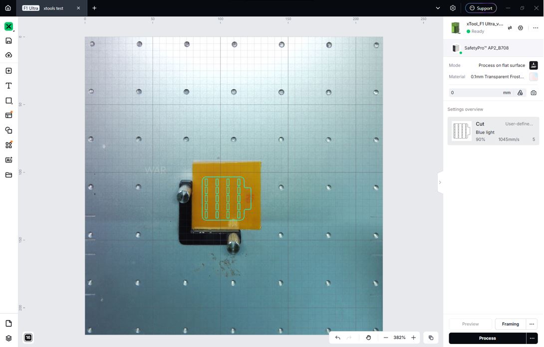
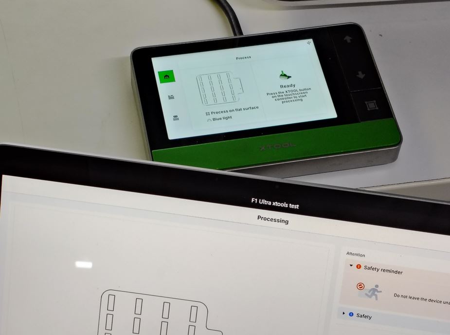
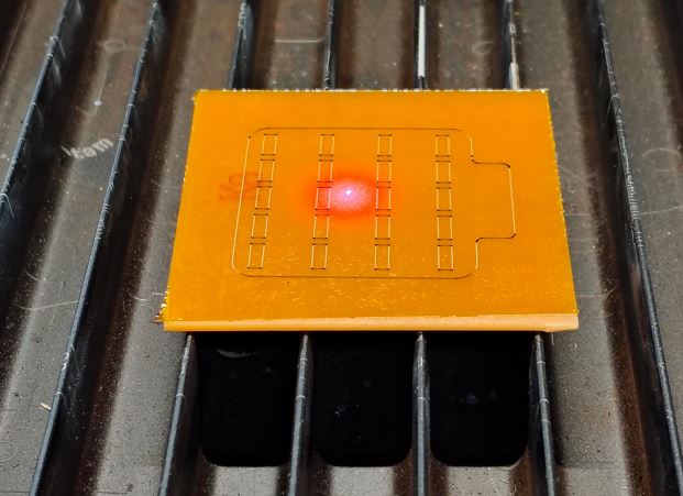
I used xTool F1 Ultra to cut the kapton tape for third layer and followed the steps in this Week 8th Group Assignment. First I downloaded, installed and open the xTool Studio 1.6.6.
We need to either convert the SVG in the xTool SW or we need to use already converted SVG using Inkspace. I already have the file that I converted to SVG using Inkscape. Now I clicked New project --> Import SVG --> Verify the Scale --> Set the frame --> set the material --> Set power 90% --> set speed between 1500-3000 --> no. of pass 5 --> repeat operation multiple time until it is you see while line on the cutting path.
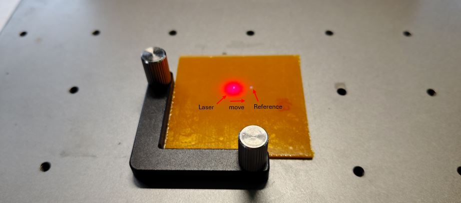
To set the focal, we need to move the red ot blue dot.
Now, I set the cutting parameters :-
- Mode : Process on flat surface
- Material : 0.1mm Transparent Material
- Process : Cut
- Power (%) : 90%
- Speed (mm/s) : 1045
- Pass : 5
Note: we cna repeat the number of passes multiple times by using external wired user control button. Thus, it is better to keep number of passes minimal in the setting.
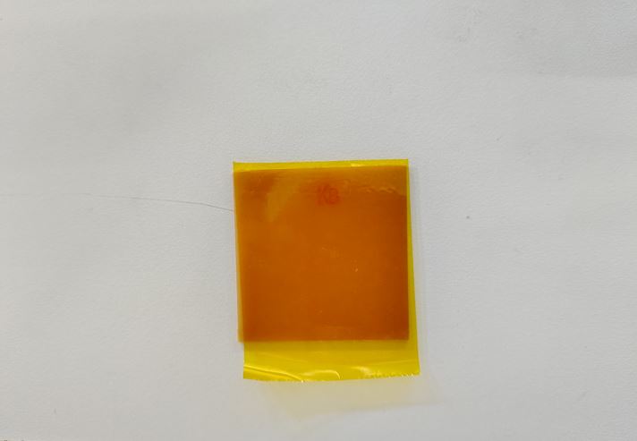
We see clear white line in below image, it indicates that kapton tape is properly cut through.
What Went Wrong -> 3-Layer PCB Fabrication
The Steps I followed are:
- First, solder the via-holes.
- Second, solder the top LED-Matrix layer.
- Third, solder the bottom layer starting with ATtiny first and then other components.
- Forth, leaser cut the Kapton Tape.
- Fifth, placed the kapton tape and soldered the third layer.
What I Learned -> Improvement in above steps
The Steps I should follow next time shall be:
- First, solder the via-holes.
- Second, leaser cut the Kapton Tape.
- Third, placed/stick the kapton tape on the PCB.
- Forth, solder the LED-Matrix and 3rd layer.
- Last, solder the bottom layer starting with ATtiny first and then other components.
Charlieplexing - Test and Validation
First install the megaTinyCore board package. In Arduino IDE go to File → Preferences → Additional Board Manager URLs and add: http://drazzy.com/package_drazzy.com_index.json. Then go to Tools → Board → Board Manager, search megaTinyCore and install it.
Connect the Board to UPDI programmer for first Power-up process to blink on board LED connect on pin PA5, make sure these settings are correct in Arduino IDE.
- Board: ATtiny1624
- Programmer: SerialUPDI - TURBO 4.5v+ 921600 Baud
- Clock: 20MHz Internal
- Chip: ATtiny1624
Then, I flashed the onboard LED Blink code.
// ATtiny1624 LED Blink
// LED connected to PA5 — Active High (LED ON when pin is HIGH)

#define LED_PIN  PIN_PA5    // define PA5 as the LED pin
                            // PIN_PA5 is the Arduino-style name for PA5 on ATtiny1624

void setup() {
  pinMode(LED_PIN, OUTPUT);     // set PA5 as output — allows us to drive current through LED
  digitalWrite(LED_PIN, LOW);   // start with LED off — ensure known state at power up
}

void loop() {
  digitalWrite(LED_PIN, HIGH);  // set PA5 HIGH — LED turns ON (Active High)
  delay(500);                   // wait 500ms — LED stays ON for 0.5 seconds

  digitalWrite(LED_PIN, LOW);   // set PA5 LOW — LED turns OFF
  delay(500);                   // wait 500ms — LED stays OFF for 0.5 seconds
                                // loop repeats forever — continuous blink
}
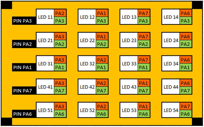
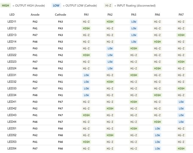
Next, I flashed the code to turn-on each Charlieplexing LEDs and for that I made below matrix to identify and ready reference of Port pins, which port pin to make High, LOW and Floating. The top pin (red/orange) is the Anode and the bottom pin (green) is the Cathode. All other pins must be set to INPUT (Hi-Z/floating) — this is the key to Charlieplexing, only 2 pins are driven at a time, all others float.
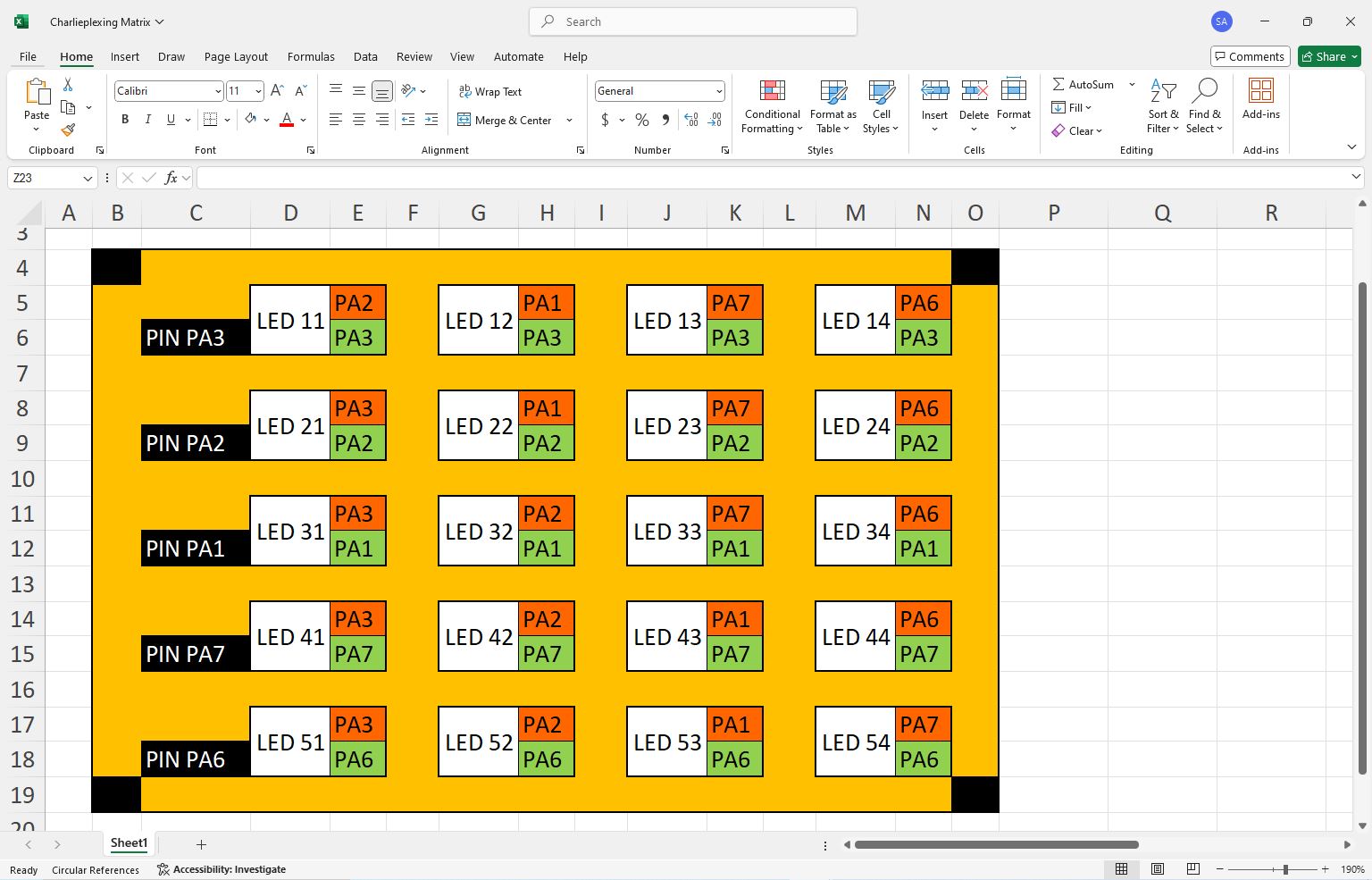
Credit Note : Belwo image, I genetated by for above excel to make AI understand the Pin connection and LED matrix.
AI prompt Claude: "Hey Claude, I want to test Charlieplexing matrix that I made on same board. it has 5 rows and 4 columns. you can refer the image, the ROW1 is connected to PA3, ROW2 is connected on PA2, ROW3 is connected on PA1, ROW4 is connected on PA7, and ROW5 is connected on PA6. Can you make a table which pins I need to make high and which low to turn -on individual LEDs? I am looking for a program in which I can call function to turn on the ELD that I want to. for example, lets give name as per matrix first led is LED11 (row 1 and column 1) similarly LED23 (row 2 and column 3), so I am having 5 Rows and 4 columns LED11 to LED54 total 20 LEDs."
This is the complete code with individual LED functions, The loop in loop() sweeps through all 20 LEDs one by one with 300ms on each.
// ATtiny1624 LED Blink
// LED connected to PA5 — Active High (LED ON when pin is HIGH)

#define LED_PIN  PIN_PA5
// ── Charlieplexing 5x4 matrix on ATtiny1624 ───────────────────────────────────
// Pins used: PA1, PA2, PA3, PA6, PA7
// LEDs named LED[row][col] — e.g. LED23 = row 2, col 3
// Charlieplex rule: only ANODE pin = OUTPUT HIGH
//                        CATHODE pin = OUTPUT LOW
//                        ALL other pins = INPUT (floating / Hi-Z)
// ─────────────────────────────────────────────────────────────────────────────

// ── Array of all 5 Charlieplex pins — used to reset all pins to Hi-Z ─────────
const uint8_t CHARLIE_PINS[] = { PIN_PA1, PIN_PA2, PIN_PA3, PIN_PA6, PIN_PA7 };
const uint8_t NUM_PINS = 5;  // total number of Charlieplex pins

// ── allOff — sets ALL pins to INPUT (Hi-Z / floating) ────────────────────────
// MUST be called before driving any LED
// prevents phantom lighting of adjacent LEDs through shared traces
void allOff() {
  for (uint8_t i = 0; i < NUM_PINS; i++) {
    pinMode(CHARLIE_PINS[i], INPUT);   // INPUT = Hi-Z = effectively disconnected
  }
}

// ── lightLED — drives one LED by setting anode HIGH and cathode LOW ───────────
// all other pins are set to INPUT (Hi-Z) by allOff() first
// anode  : the pin connected to the + side of the LED
// cathode: the pin connected to the - side of the LED
void lightLED(uint8_t anode, uint8_t cathode) {
  allOff();                            // first float ALL pins — prevents ghosting

  pinMode(anode,   OUTPUT);            // set anode pin as output
  pinMode(cathode, OUTPUT);            // set cathode pin as output

  digitalWrite(anode,   HIGH);         // drive anode HIGH — current source
  digitalWrite(cathode, LOW);          // drive cathode LOW — current sink
                                       // current flows anode → LED → cathode → LED lights up
}

// ── Individual LED functions ──────────────────────────────────────────────────
// Row 1 (PIN_PA3 = cathode for all row 1 LEDs)
void LED11() { lightLED(PIN_PA2, PIN_PA3); }  // anode=PA2, cathode=PA3
void LED12() { lightLED(PIN_PA1, PIN_PA3); }  // anode=PA1, cathode=PA3
void LED13() { lightLED(PIN_PA7, PIN_PA3); }  // anode=PA7, cathode=PA3
void LED14() { lightLED(PIN_PA6, PIN_PA3); }  // anode=PA6, cathode=PA3

// Row 2 (PIN_PA2 = cathode for all row 2 LEDs)
void LED21() { lightLED(PIN_PA3, PIN_PA2); }  // anode=PA3, cathode=PA2
void LED22() { lightLED(PIN_PA1, PIN_PA2); }  // anode=PA1, cathode=PA2
void LED23() { lightLED(PIN_PA7, PIN_PA2); }  // anode=PA7, cathode=PA2
void LED24() { lightLED(PIN_PA6, PIN_PA2); }  // anode=PA6, cathode=PA2

// Row 3 (PIN_PA1 = cathode for all row 3 LEDs)
void LED31() { lightLED(PIN_PA3, PIN_PA1); }  // anode=PA3, cathode=PA1
void LED32() { lightLED(PIN_PA2, PIN_PA1); }  // anode=PA2, cathode=PA1
void LED33() { lightLED(PIN_PA7, PIN_PA1); }  // anode=PA7, cathode=PA1
void LED34() { lightLED(PIN_PA6, PIN_PA1); }  // anode=PA6, cathode=PA1

// Row 4 (PIN_PA7 = cathode for all row 4 LEDs)
void LED41() { lightLED(PIN_PA3, PIN_PA7); }  // anode=PA3, cathode=PA7
void LED42() { lightLED(PIN_PA2, PIN_PA7); }  // anode=PA2, cathode=PA7
void LED43() { lightLED(PIN_PA1, PIN_PA7); }  // anode=PA1, cathode=PA7
void LED44() { lightLED(PIN_PA6, PIN_PA7); }  // anode=PA6, cathode=PA7

// Row 5 (PIN_PA6 = cathode for all row 5 LEDs)
void LED51() { lightLED(PIN_PA3, PIN_PA6); }  // anode=PA3, cathode=PA6
void LED52() { lightLED(PIN_PA2, PIN_PA6); }  // anode=PA2, cathode=PA6
void LED53() { lightLED(PIN_PA1, PIN_PA6); }  // anode=PA1, cathode=PA6
void LED54() { lightLED(PIN_PA7, PIN_PA6); }  // anode=PA7, cathode=PA6

// ── setup ─────────────────────────────────────────────────────────────────────
void setup() {
  allOff();                            // start with all pins floating — safe initial state
}

// ── loop — demo: light each LED one by one ────────────────────────────────────
void loop() {
  // Row 1
  LED11(); delay(300);
  LED12(); delay(300);
  LED13(); delay(300);
  LED14(); delay(300);

  // Row 2
  LED21(); delay(300);
  LED22(); delay(300);
  LED23(); delay(300);
  LED24(); delay(300);

  // Row 3
  LED31(); delay(300);
  LED32(); delay(300);
  LED33(); delay(300);
  LED34(); delay(300);

  // Row 4
  LED41(); delay(300);
  LED42(); delay(300);
  LED43(); delay(300);
  LED44(); delay(300);

  // Row 5
  LED51(); delay(300);
  LED52(); delay(300);
  LED53(); delay(300);
  LED54(); delay(300);

  allOff(); delay(500);                // brief pause with all LEDs off before repeating
}
Note: Charlieplexing can only light one LED at a time. If I want to display multiple LEDs simultaneously I need to multiplex them rapidly (cycle through each one faster than ~1ms each) so they appear on simultaneously to the eye. Below, is the multiplexing code — it rapidly cycles through all LEDs I want ON so fast (every 500µs per LED) that my eye sees them all as simultaneously lit.
The key concept in this code: Instead of delay() in the main loop, every waiting period now uses a while (millis() - start < duration) loop that keeps calling multiplex() continuously. This is critical — if I ever put a plain delay() while LEDs should be on, the multiplexing stops and only one LED stays lit while the rest go dark.
To use setLED( ) in my own patterns:
setLED(2, 3, true); // turn LED23 ON — row 2, col 3
setLED(2, 3, false); // turn LED23 OFF — row 2, col 3
clearAll(); // turn ALL LEDs off instantly
// ── Charlieplexing 5x4 matrix on ATtiny1624 with multiplexing ────────────────
// Pins: PA1, PA2, PA3, PA6, PA7
// Multiplexing: cycles through active LEDs rapidly — eye sees all as ON together
// Each LED gets 500µs on-time per cycle — at 20 LEDs max = 10ms full cycle = 100Hz
// ─────────────────────────────────────────────────────────────────────────────

// ── Pin array — all 5 Charlieplex pins ───────────────────────────────────────
const uint8_t CHARLIE_PINS[] = { PIN_PA1, PIN_PA2, PIN_PA3, PIN_PA6, PIN_PA7 };
const uint8_t NUM_PINS = 5;            // total number of Charlieplex pins

// ── LED descriptor — stores anode and cathode pin for each LED ────────────────
struct LED {
  uint8_t anode;                       // pin to drive HIGH to light this LED
  uint8_t cathode;                     // pin to drive LOW to light this LED
};

// ── Full LED lookup table — all 20 LEDs defined by anode/cathode pair ─────────
const LED LED_TABLE[5][4] = {
  // Col1          Col2          Col3          Col4
  { {PIN_PA2, PIN_PA3}, {PIN_PA1, PIN_PA3}, {PIN_PA7, PIN_PA3}, {PIN_PA6, PIN_PA3} }, // Row 1
  { {PIN_PA3, PIN_PA2}, {PIN_PA1, PIN_PA2}, {PIN_PA7, PIN_PA2}, {PIN_PA6, PIN_PA2} }, // Row 2
  { {PIN_PA3, PIN_PA1}, {PIN_PA2, PIN_PA1}, {PIN_PA7, PIN_PA1}, {PIN_PA6, PIN_PA1} }, // Row 3
  { {PIN_PA3, PIN_PA7}, {PIN_PA2, PIN_PA7}, {PIN_PA1, PIN_PA7}, {PIN_PA6, PIN_PA7} }, // Row 4
  { {PIN_PA3, PIN_PA6}, {PIN_PA2, PIN_PA6}, {PIN_PA1, PIN_PA6}, {PIN_PA7, PIN_PA6} }, // Row 5
};

// ── Active LED buffer — stores which LEDs are currently ON ────────────────────
// each entry stores row(0-4) and col(0-3) of an active LED
struct ActiveLED {
  uint8_t row;                         // row index 0–4
  uint8_t col;                         // col index 0–3
};

ActiveLED activeBuffer[20];            // maximum 20 LEDs can be active at once
uint8_t   activeCount = 0;             // how many LEDs are currently in buffer

// ── allOff — float all pins to Hi-Z ──────────────────────────────────────────
void allOff() {
  for (uint8_t i = 0; i < NUM_PINS; i++) {
    pinMode(CHARLIE_PINS[i], INPUT);   // INPUT = Hi-Z = electrically disconnected
  }
}

// ── setLED — add or remove an LED from the active buffer ─────────────────────
// row: 1–5, col: 1–4, state: true=ON, false=OFF
void setLED(uint8_t row, uint8_t col, bool state) {
  uint8_t r = row - 1;                 // convert 1-based to 0-based index
  uint8_t c = col - 1;                 // convert 1-based to 0-based index

  if (state) {                         // turning LED ON — add to buffer
    for (uint8_t i = 0; i < activeCount; i++) {
      if (activeBuffer[i].row == r && activeBuffer[i].col == c) {
        return;                        // already in buffer — do not add duplicate
      }
    }
    if (activeCount < 20) {            // buffer not full
      activeBuffer[activeCount].row = r;   // store row index
      activeBuffer[activeCount].col = c;   // store col index
      activeCount++;                   // increment active LED count
    }
  } else {                             // turning LED OFF — remove from buffer
    for (uint8_t i = 0; i < activeCount; i++) {
      if (activeBuffer[i].row == r && activeBuffer[i].col == c) {
        // shift remaining entries down to fill the gap
        for (uint8_t j = i; j < activeCount - 1; j++) {
          activeBuffer[j] = activeBuffer[j + 1];
        }
        activeCount--;                 // reduce active count
        return;
      }
    }
  }
}

// ── clearAll — turn off all LEDs and empty the active buffer ─────────────────
void clearAll() {
  activeCount = 0;                     // empty the buffer — no LEDs active
  allOff();                            // float all pins immediately
}

// ── multiplex — call this repeatedly in loop — drives active LEDs ─────────────
// cycles through each active LED, lights it for 500µs, then moves to next
// at 500µs per LED, 20 LEDs = 10ms full cycle = 100Hz refresh — flicker free
void multiplex() {
  if (activeCount == 0) {              // no LEDs to show
    allOff();                          // make sure everything is off
    return;
  }

  for (uint8_t i = 0; i < activeCount; i++) {
    uint8_t r = activeBuffer[i].row;   // get row index of this LED
    uint8_t c = activeBuffer[i].col;   // get col index of this LED

    LED led = LED_TABLE[r][c];         // look up anode and cathode pins

    allOff();                          // float all pins before switching
    pinMode(led.anode,   OUTPUT);      // set anode pin as output
    pinMode(led.cathode, OUTPUT);      // set cathode pin as output
    digitalWrite(led.anode,   HIGH);   // drive anode HIGH — current source
    digitalWrite(led.cathode, LOW);    // drive cathode LOW — LED lights up

    delayMicroseconds(500);            // hold this LED on for 500µs
                                       // shorter = dimmer but smoother at high count
                                       // longer = brighter but may flicker with many LEDs
  }

  allOff();                            // float all pins at end of cycle
}

// ── setup ─────────────────────────────────────────────────────────────────────
void setup() {
  allOff();                            // start safe — all pins floating
}

// ── loop — demo showing multiplexing capability ───────────────────────────────
void loop() {

  // ── Demo 1 — light all 20 LEDs simultaneously ──────────────────────────────
  clearAll();                          // clear buffer
  for (uint8_t r = 1; r <= 5; r++) {  // loop through all rows
    for (uint8_t c = 1; c <= 4; c++) {// loop through all columns
      setLED(r, c, true);              // add every LED to active buffer
    }
  }
  unsigned long start = millis();      // record start time
  while (millis() - start < 3000) {   // run for 3 seconds
    multiplex();                       // keep multiplexing — all 20 LEDs appear ON
  }

  // ── Demo 2 — light only specific LEDs simultaneously ───────────────────────
  clearAll();                          // clear all LEDs
  setLED(1, 1, true);                  // LED11 ON
  setLED(2, 3, true);                  // LED23 ON
  setLED(3, 2, true);                  // LED32 ON
  setLED(4, 4, true);                  // LED44 ON
  setLED(5, 1, true);                  // LED51 ON
  start = millis();
  while (millis() - start < 3000) {   // show for 3 seconds
    multiplex();                       // multiplex — 5 LEDs appear simultaneously ON
  }

  // ── Demo 3 — chase pattern using multiplexing ───────────────────────────────
  clearAll();
  for (uint8_t r = 1; r <= 5; r++) {
    for (uint8_t c = 1; c <= 4; c++) {
      setLED(r, c, true);              // add LED to active set
      start = millis();
      while (millis() - start < 200) {// show current set for 200ms
        multiplex();                   // multiplex all currently active LEDs
      }
    }
  }

  // ── Demo 4 — row by row wipe ON then OFF ────────────────────────────────────
  clearAll();
  for (uint8_t r = 1; r <= 5; r++) {  // light one full row at a time
    for (uint8_t c = 1; c <= 4; c++) {
      setLED(r, c, true);              // turn on all 4 LEDs in this row
    }
    start = millis();
    while (millis() - start < 500) {  // hold each row for 500ms
      multiplex();
    }
  }
  start = millis();
  while (millis() - start < 1000) {   // show all rows on together for 1 sec
    multiplex();
  }
  clearAll();                          // wipe all off
  delay(500);                          // pause before repeating
}
Key Learnings This Week
- NeoPixel 1-wire protocol (daisy chain)
- Charlieplexing Concept
- XTool fiber laser Cutting
- Double Layer PCB Milling
- Third layer of PCB on Kapton tape
- Concept of LED Multiplexing in Charlieplexing
Downloads
- Charlieplexing PCB KiCad Design files
- Charlieplexing PCB Gerber files
- Charlieplexing PCB PNG files
- PCB Layer 3 SVG file for Laser Cut of Kapton Tape
Useful Links
Reflection
Where I can improve because as per our regional instructor we are clearly lagging from last two weeks. I need to make my design ready before Sunday, so that I can mill the PCB and test on Monday and Tuesday. This week I was not able to complete Testing before Global class because I designed my PCB on Monday milled on Tuesday and added third layer on Wednesday. Thus I was not able to test and validate it.