What I did in Week 06
In my assignment this week I will design a development board using an Attiny 412 microcontroller and several electronic components which together will allow me to perform various tasks with that board. I will do the entire design using an EDA tool, in this case the KiCAD software that allows me to do electronic design and PCB board design.
- EDA: Electronic Design Automation
- Group: use the test equipment in your lab to observe the operation of an embedded microcontroller
- Individual: use an EDA tool to design an embedded microcontroller system using parts from the inventory, and check its design rules for fabrication.
- Extra credit: simulate a circuit
- Extra credit: try another design workflow
- Extra credit: design a case
Group page
Group page link
ATtiny412
Step 1 ·
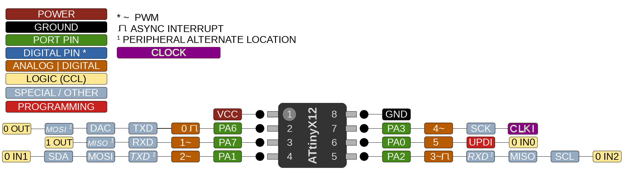
The ATtiny412 is an 8-bit microcontroller based on the AVR architecture. This microcontroller is designed for applications requiring low power consumption and a small footprint. This chip has 8 pins, 4 KB of flash memory, 256 bytes of SRAM, and uses the UPDI interface for single-pin programming and debugging.
Step 2 ·
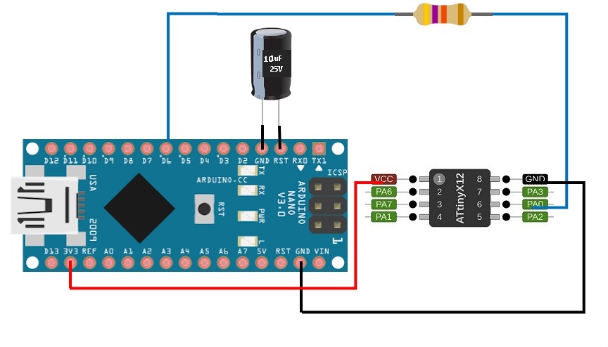
To upload the code we created, it is necessary to do so through the UPDI(6) port and using an Arduino Nano, as shown in the diagram.
kiCAD
3D scanning has several applications, one of which is reverse engineering. Another application, which I will demonstrate, is scanning an object or person, and here I will show all the steps to achieve this.

Step 1 ·
We installed the KiCad software, which is free and easy to install.
Step 2 ·
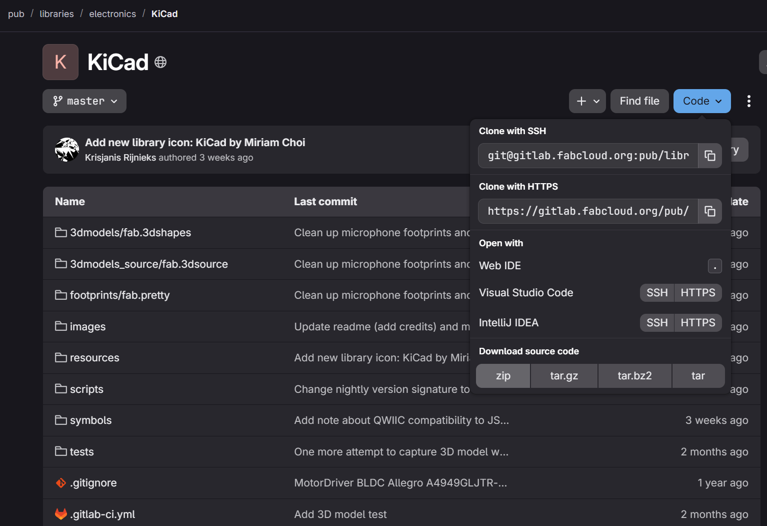
One advantage of this software is that it includes a library of most of the electronic components used in Fab Academy. We'll proceed with downloading this library in .zip format. The link for the library is https://gitlab.fabcloud.org/pub/libraries/electronics/kicad. Then, extract the folder to a specific location on your computer.
Step 3 ·
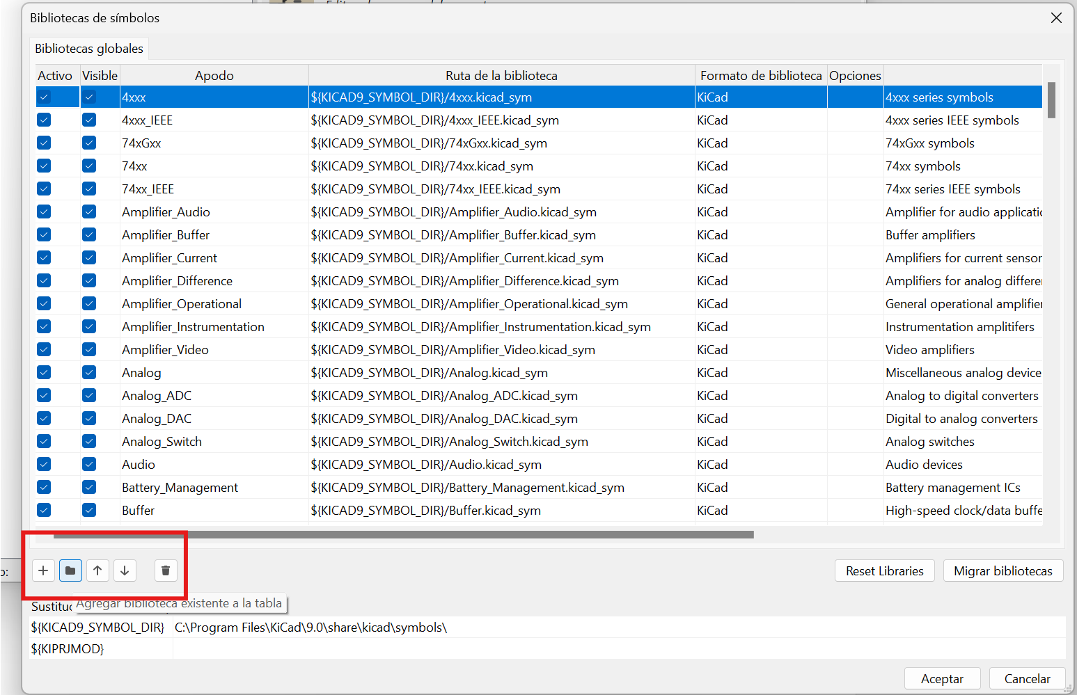
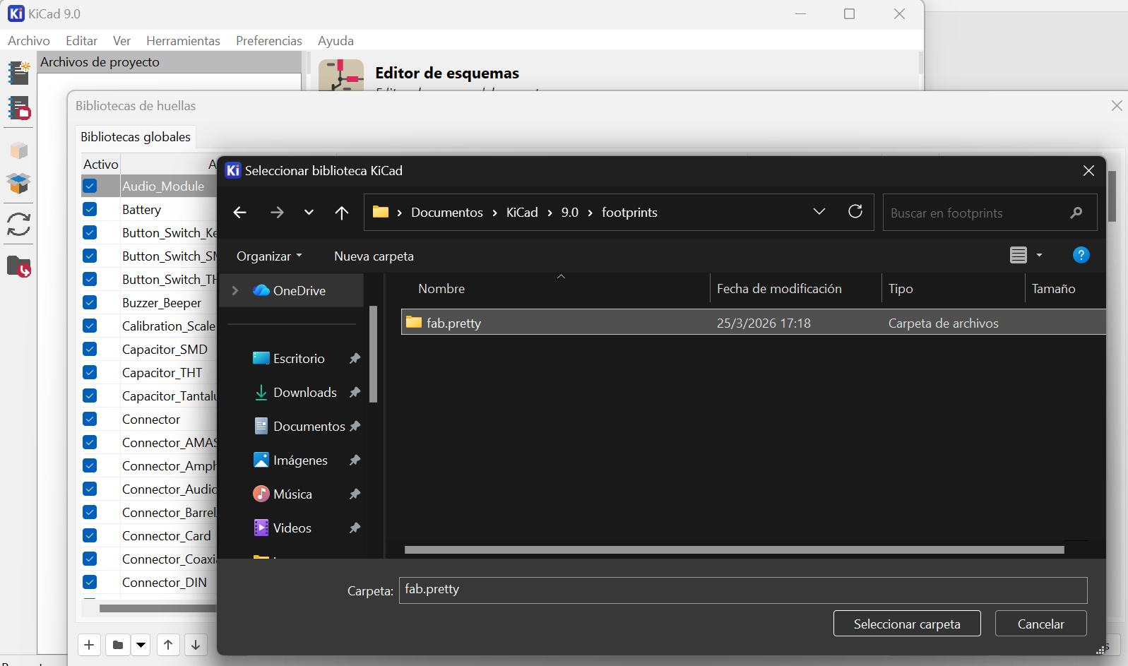
We're going to add the libraries to our KiCad software. To do this, open the software and go to Preferences – Manage Symbol Library. As shown in the image, add the file path fab.kicad_sym and add
Step 4 ·
To add the fingerprint library, follow the same process, but select Preferences—Manage fingerprint libraries, locate the folder, and add it.
Step 5 ·
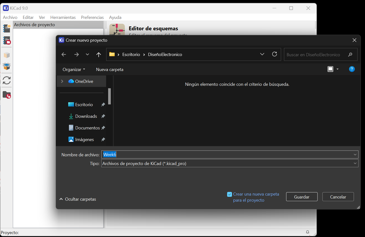
Now we open the software and create a new project and save the project in a folder on our computer.
Step 6 ·
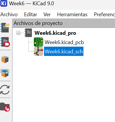
We open the empty file with the .sch extension so we can begin with our schematic diagram.
Step 7 ·
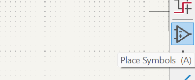
On the right side we choose the icon that says PLACE SYMBOLS where all the components we can use are located, including those from the FAB library that we imported.
Step 8 ·
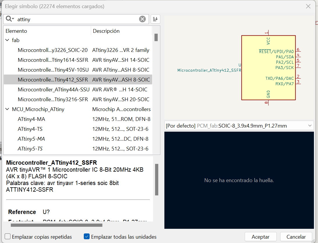
We look for the components we are going to use and select them to add to the workspace.
Step 9 ·
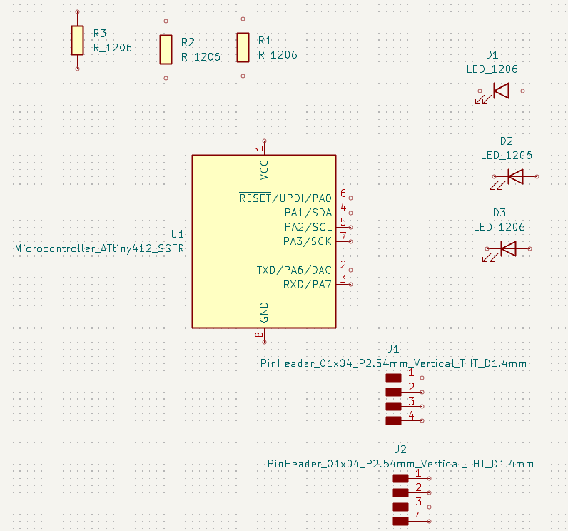
This is what all the added components we're going to use look like; they're all from the FAB library.
Step 10 ·
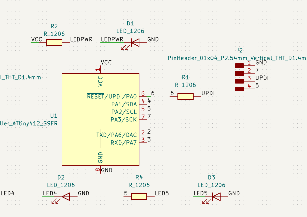
We placed labels on each electronic component indicating how they will be connected to each other.
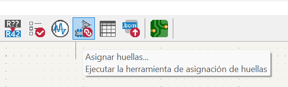
Step 11 ·
We must enter the icon shown in the image to verify that the fingerprints are assigned.
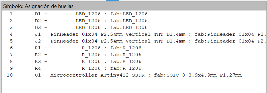
Step 12 ·
We must verify that all elements have their corresponding footprint; otherwise, we must assign it by searching in the specific library.
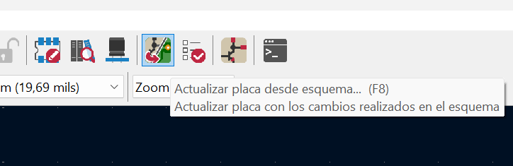
Step 13 ·
On the PCB board page, we need to update it so that it shows us all the components with the connections they should have.
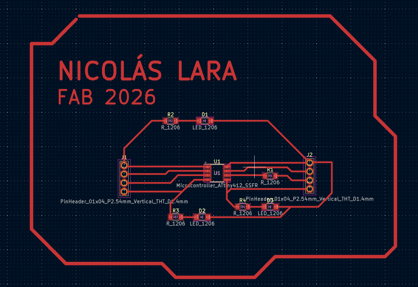
Step 14 ·
We made all the connections with the appropriate trace width and following electronic design rules. The circuit I designed is a microcontroller that has integrated LEDs on ports 4 and 5 to show the behavior of the outputs. Port 6 has the resistor for uploading the code via the UPDI port, and it also has an LED to indicate whether it is powered on.
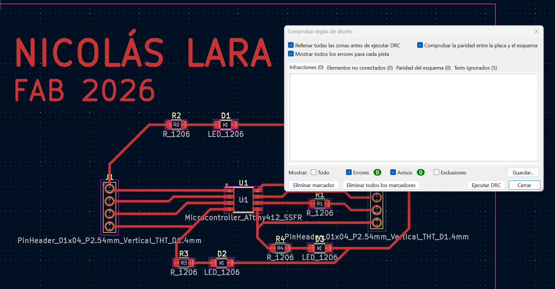
Step 15 ·
We performed a verification to ensure the board had no errors in the traces and could be manufactured. This was done using a DRC tool within the KiCad software, which confirmed that our design was error-free.
Conclusions
In this assignment, I gained a solid understanding of the fundamentals of electronic design and the steps involved in creating a custom PCB. Through schematic design and board layout development, I learned how electronic components are connected and arranged to create functional circuits. Most importantly, I grasped the significance of component selection, trace organization, and proper routing to ensure a reliable, manufacturable board. I also improved my skills with electronic design software and gained a deeper understanding of how digital schematics are transformed into physical electronic systems. This assignment strengthened my problem-solving abilities by requiring constant verification of connections, dimensions, and design rules before fabrication.
← Main Page