Week 8 – Electronics Production
Group Assignment
Individual Assignment
Make and test a microcontroller development board that you designed.
I'll be honest: I went into this week thinking "how hard can it be to mill a little board?" Spoiler: harder than it looks. But I got there, and the board works, and I only had to mill it approximately one million times. Let's get into it.
The Board: Freezer Thermometer
Rather than making a generic blink board that would immediately collect dust, I decided to build something I'd actually use — a wireless freezer thermometer with a DS18B20 temperature probe, a status LED, and a XIAO ESP32-C3 microcontroller. This also conveniently doubles as my Week 9 input device assignment, because efficiency is a virtue.
Components: - Seeed XIAO ESP32-C3 (castellated edge pads, soldered directly to the board) - DS18B20 waterproof temperature probe - 4.7kΩ pull-up resistor (0805) - 330Ω current-limiting resistor for status LED (0805) - Red LED (0805) - 100µF decoupling capacitor (0805)
PCB Design in KiCad 9
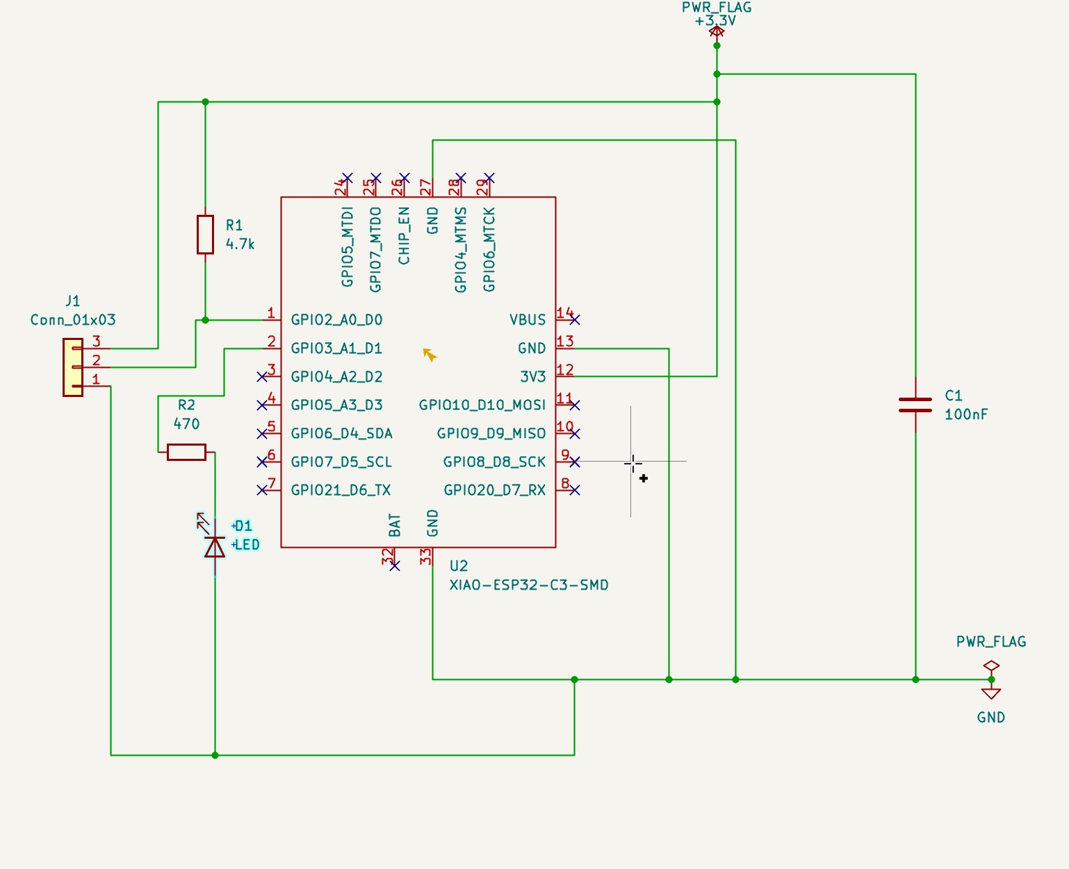
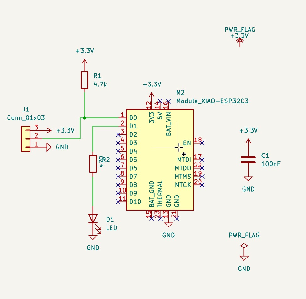
Schematic
I started with the XIAO ESP32-C6 symbol since that's my manta ray chip and I am comfortable with it.
Then I realized I had extra ESP32-C3s onhand and since I didn't have confidence in my soldering skills I elected to go with that.
The pin mapping is nearly identical so the swap in KiCad was straightforward: right-click the symbol -> Change Symbol -> select XIAO-ESP32-C3 -> check Update symbol fields and Update footprint.
Key wiring decisions per Claude AI:
- DS18B20 data line -> GPIO D0 with 4.7kΩ pull-up to 3.3V (required for the 1-Wire protocol)
- Status LED -> GPIO D1 through 330Ω resistor
- Decoupling cap between 3.3V and GND, placed close to the XIAO
I ran ERC and got to zero errors (with one footprint library warning that I chose to ignore after Claude AI said it was okay).
original schematic with wires
This schematic was extremely untidy so I researched how other people displayed their nets. I found that if a component goes to GND, don't draw the wire to GND,
just place the GND symbol at the component connection. It keeps the schematic neat and easy to read.
revised schematic with minimal wires
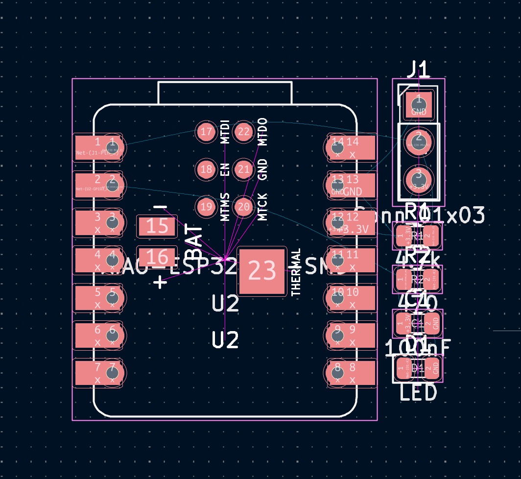
Footprint Assignment
All components except for the microcontroller uses 0805 SMD packages. Per Claude that is a good size to use on a milled board. I remain skeptical.
I used the Seeed_Studio_XIAO_ESP32C3 footprint from the library. The DS18B20 connector uses
Connector_JST:JST_PH_S3B-PH (3-pin SMD JST PH 2.0mm).
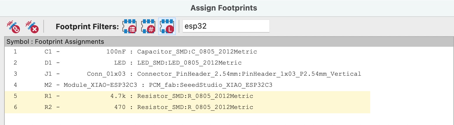
footprint assignments
PCB Layout
I placed components using the ratsnest lines. I started with the ESP32C3, the pull-up resistor and status LED are positioned nearby so trace routing stays short and sensible. The decoupling cap lives as close to the XIAO's power pins as I could manage without things getting chaotic.
DRC came back clean (zero errors, silkscreen warnings only — not a problem for a milled board since we don't have silkscreen anyway).
this included J1 as through-hole
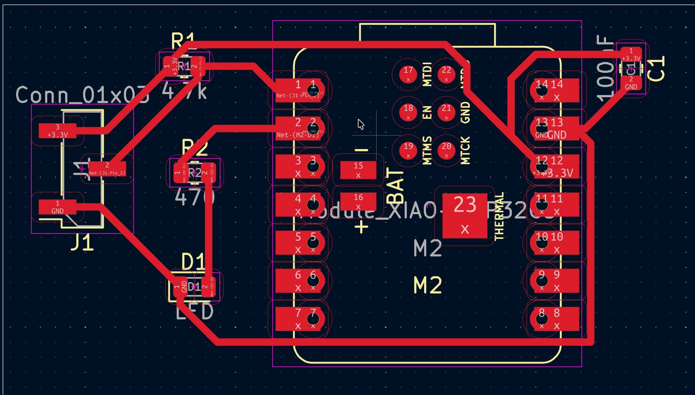
this included J1 as SMD pads
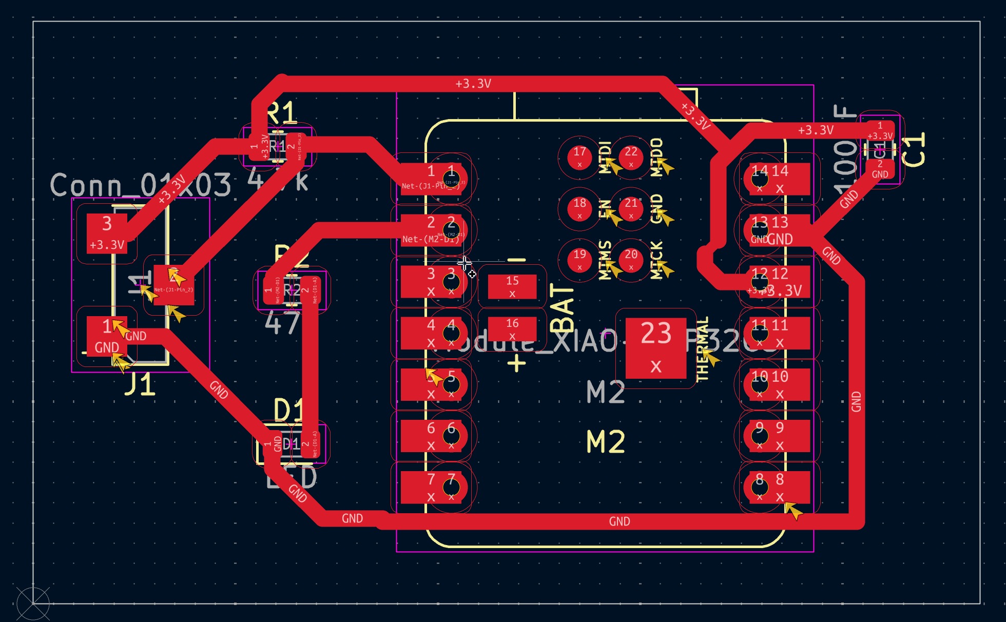
thicker trace lines for easier soldering
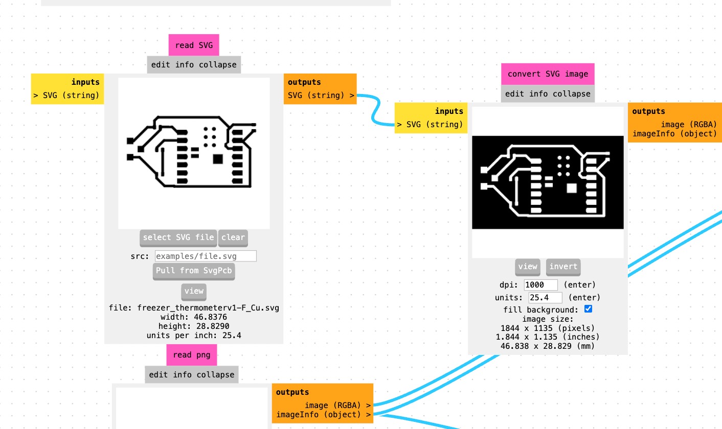
SVG Export for Mods
File -> Plot -> SVG, with these settings: - Fit page to board area — if you forget this, mods sees an A4 page and your board appears the size of a postage stamp in the middle of it. Ask me how I know. - Black and white mode - Plot F.Cu layer and Edge.Cuts layer separately
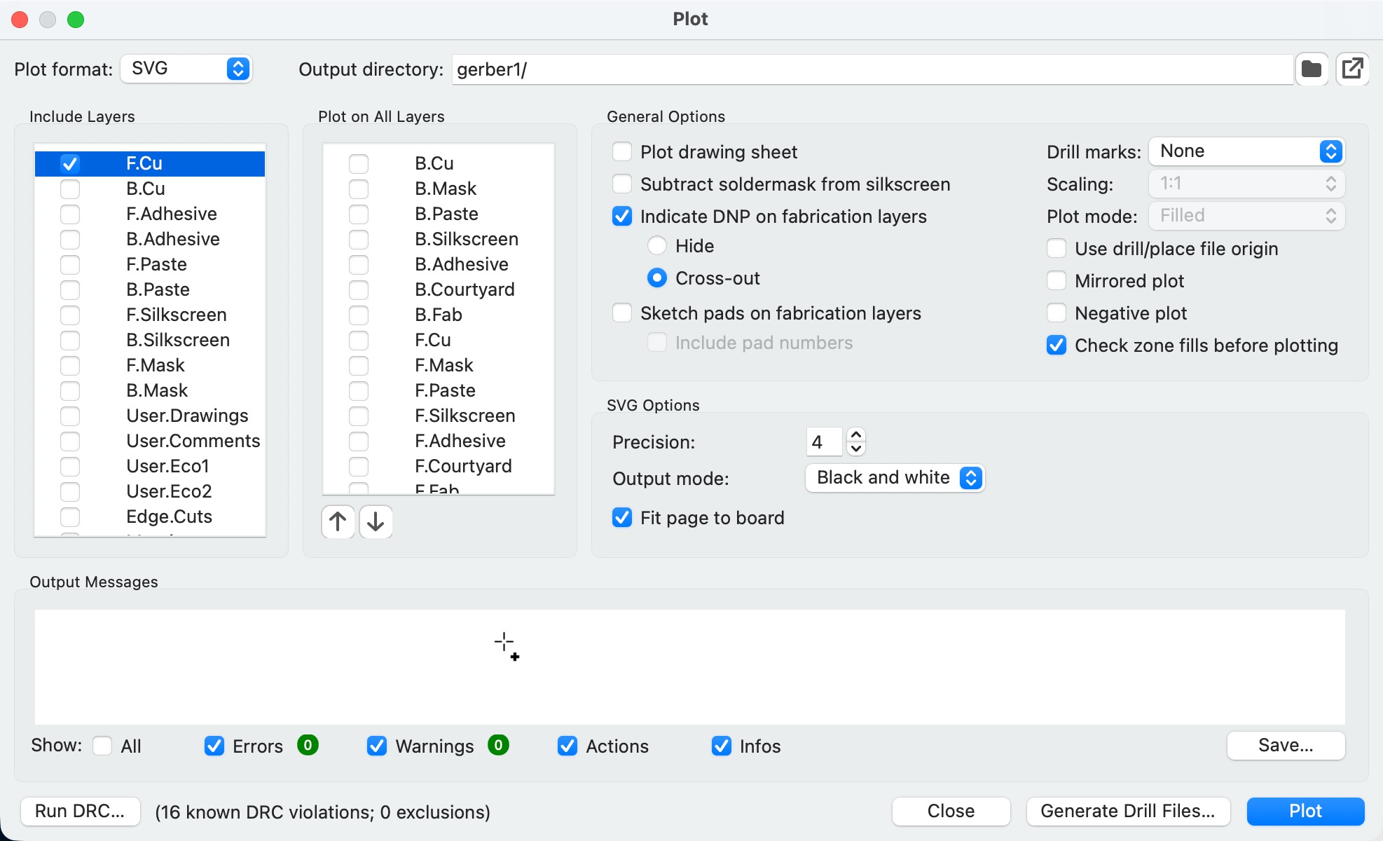
settings used for F.Cu plot in SVG format
Toolpath Generation with Mods CE
Thank goodness I was able to go to the Saturday class that introduced us to Mods Project. Rico gave us
some helpful hints on how to get started or I would have been overwhelmed.
Traces (F.Cu)
To create the code needed go to Programs -> G-code -> mill 2D PCB
Load the F.Cu SVG. that was exported from KiCad and invert it so the part you want to keep is white.
Settings used for the toolpath:
| Parameter | Value |
|---|---|
| Tool | 30° V-bit, 0.1mm tip |
| Cut depth | 0.1mm |
| Max depth | 0.1mm |
| Feed rate | 2 mm/s |
| Offsets | 4 |
| Stepover | 0.5 |
| Direction | Conventional |
Mods CE interface showing trace toolpath settings
Click Calculate once you enter you tool information.
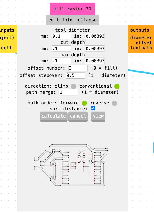
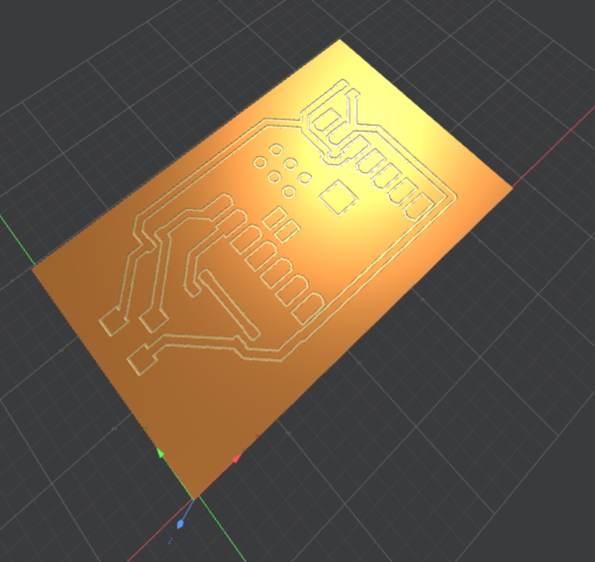
Mill raster 2D
A 3D version of the board will open up.
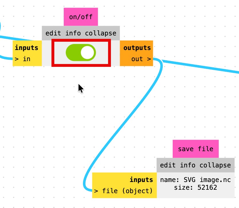
Also, when the on/off toggle is on your .nc file will download.
Outline (Edge.Cuts)
| Parameter | Value |
|---|---|
| Tool | 0.8mm corn end mill |
| Cut depth | 0.6mm per pass |
| Max depth | 1.7mm |
| Feed rate | 2 mm/s |
| Offsets | 3 |
| Direction | Conventional |
Both NC files were downloaded: one for traces, one for outline.
Milling on the Genmitsu 3018 Pro V2
Machine Setup
- FR1 copper clad, 1.4mm thick, taped flat to MDF spoilboard with double-sided tape
- Jog the X and Y axis to the corner of the board.
- Z probe: alligator clip to bit and a base with a metal disc in the center of the base. It is wired to the controller.
Initial Attempts and the Chaos That Followed
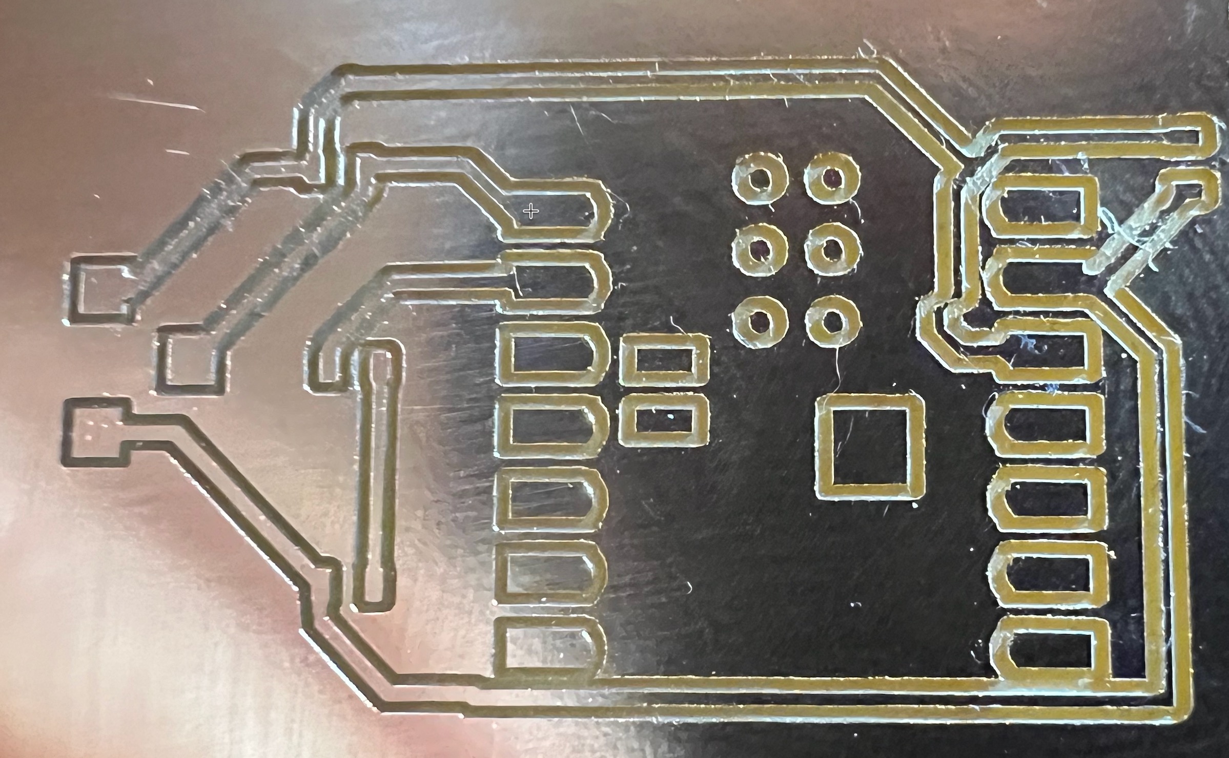
Attempt 1: Cut depth 0.05mm. Result: Some traces cut fine, others barely visible, a few areas untouched entirely. Root cause: board not perfectly flat, Z probed at one point only, and at 0.05mm there is zero tolerance for any surface variation whatsoever.
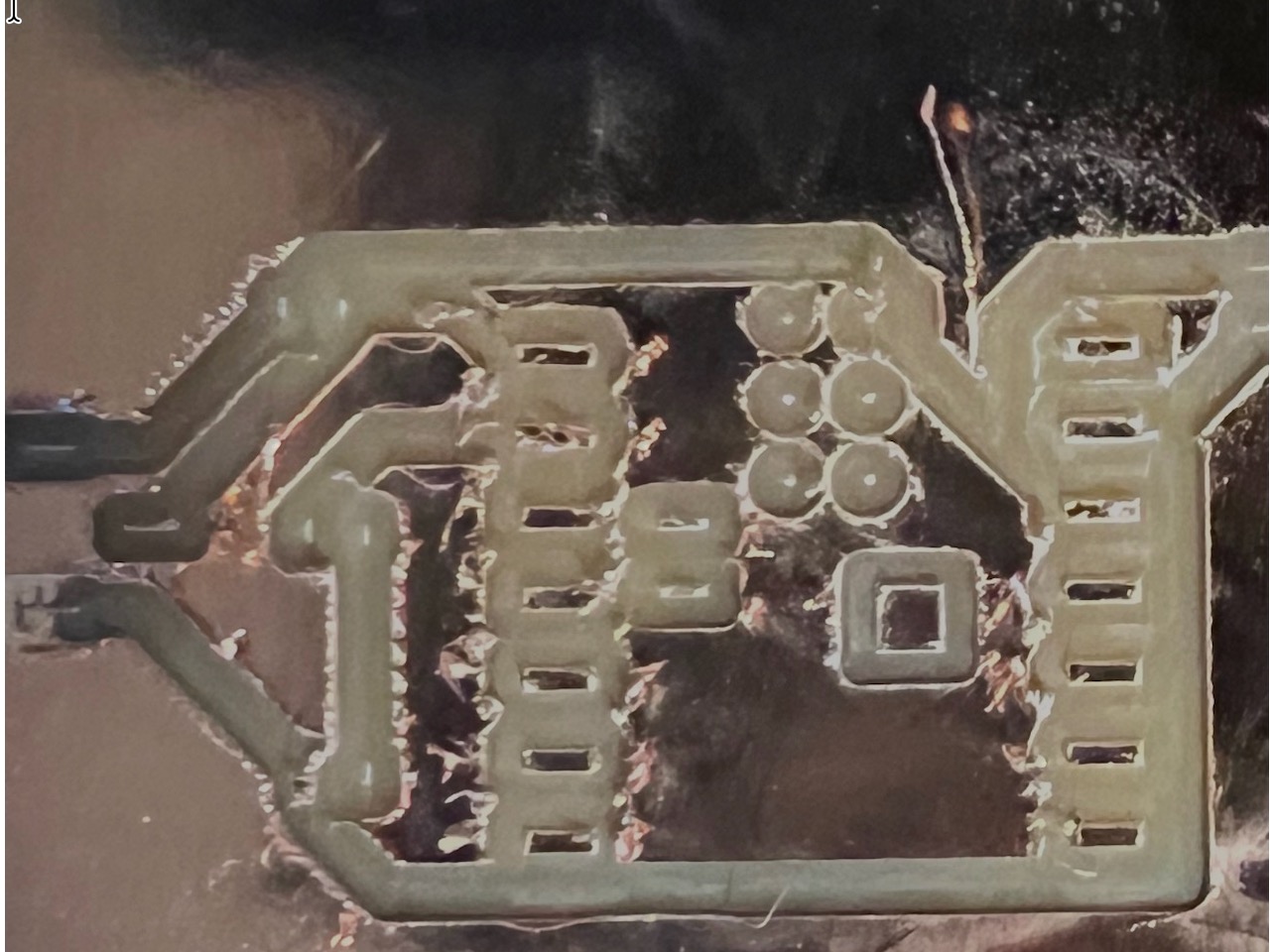
First board milled - used it to practice soldering the pads
Attempt 2: Increased to 0.1mm. This was too much. It dug into the board too much! Unfortunately I made two changes with this test. I used a board from a different batch AND increased to 0.1mm.
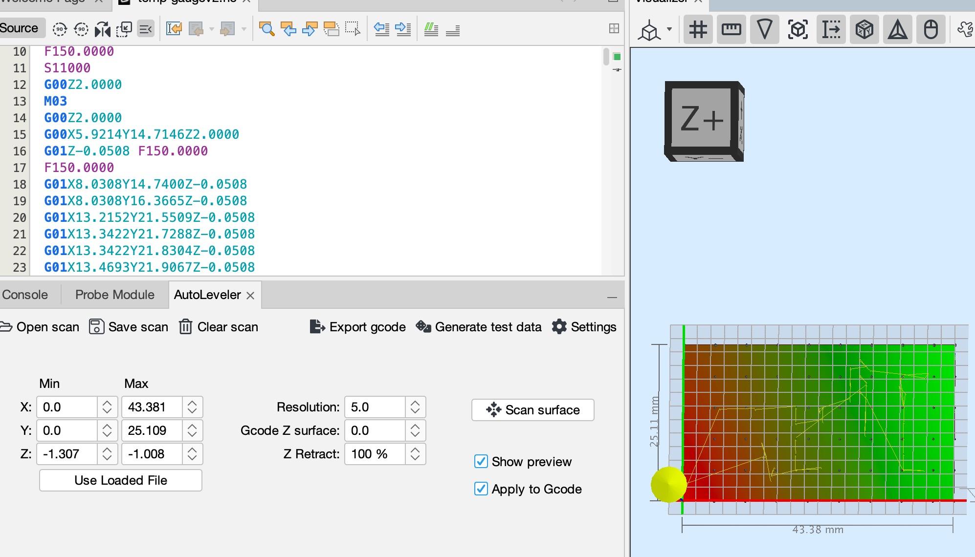
UGS Auto Leveler
Instead of probing a single Z point and hoping for the best, Auto Leveler probes a grid across the entire board surface and compensates the G-code Z values in real time.
Auto Leveler workflow:
- Home the machine (
$H) - Jog to front-left corner of board -> Zero X and Y
- Jog Z to approximately 0.5mm above surface -> Zero Z
- Connect probe (alligator clip to collet, clip to copper surface)
- Open Machine → Auto Leveler
- Click Use Loaded File (loads your trace NC file)
- Set Resolution: 5.0mm
- Set Z Min: -5, Z Max: 2.0, Z Retract: 50%
- Click Scan — watch it probe a grid across the surface
- Click Save scan (in case you need to re-run)
- Click Apply to G-code
- Click Export G-code — save as a new file
- Load that exported file in UGS and run it
I ran auto-leveling several times without much success
The first scan attempt I ran had an error — I had zeroed Z too high and the scan showed a flat plane rather than actual surface variation. According to Claude, the key is to zero Z at the surface properly before scanning: jog down until the bit is just barely touching (or use the Z probe), then zero. I used the Z probe. On the second attempt the scan correctly showed the board tilting slightly (left side ~0.3mm lower than right), and the corrected G-code had Z values ranging from -0.05mm to -0.35mm to compensate.
I was getting a little lax about hanging around while the milling took place, but I learned why that is highly discouraged. The milling bit worked loose while running and somehow jammed into the board. I quickly hit stop and amazingly the bit wasn't damaged.
Final Successful Mill
I gave up on auto-leveling because each time the bit never touched the left side of the board and I was wasting too much time. I went back to the single z probe and .1 milling depth. I will revisit auto-leveling at another time. Once I figure it out I know it will be very useful. I verified the isolation channels with a multimeter. I didn't have any shorts and had continuity on the traces.
Milled board ready for solder
Soldering
Surface Preparation
Per Claude, milled FR1 boards oxidize fast. It recommended I scuff the surface lightly with 400-grit sandpaper to break through oxidation. I didn't feel like looking for sandpaper so I just rolled with what I had. It had been a while since I soldered so I used one of the failed milled board to get into rhythm. I added flux and tinned the pads. This is probably short-sided, but for the ESP32-C3 I only tinned the pads I was using. I didn't want to take a chance shorting the board any more than I had to.
Soldering Order and Technique
Per Claude, order matters: smallest/lowest profile components first, the big XIAO module last.
- 0805 resistors
- 0805 capacitor
- 0805 LED
- JST connector - no connector, just pads
- XIAO ESP32-C3 (castellated pads last)
I did not follow that advice. I started with the ESP32-C3.
Technique: - Iron temp: 670°F (started at 750°F — too hot; 670°F gave dramatically better joints) - Flux first on pads, especially castellated pads - Tack one end of each component first, check alignment, then solder the other end - For castellated pads: tin the pads on the board first, place XIAO, then reflow with iron touching both the pad on the board and the castellated pad on the XIAO
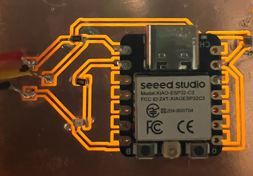
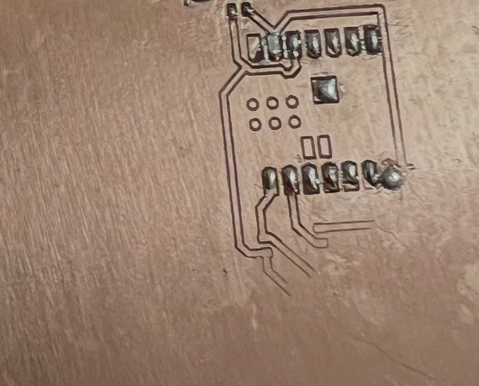
Solderd board
Continuity Check
After soldering: multimeter continuity check across all traces before powering up. Found one suspicious joint on the LED resistor — reflowed it with fresh flux and it cleaned right up.
Programming and Testing
Arduino IDE Setup
- Board: XIAO_ESP32C3 (not generic ESP32-C3 — the specific XIAO target gives correct pin mapping)
- This is important: on the XIAO ESP32-C3, the physical labels D0 and D1 correspond to internal GPIO2 and GPIO3 respectively. Using the wrong board target in Arduino IDE will give you wrong pin assignments and you'll sit there wondering why your LED doesn't blink. The pin mapping confusion bit me briefly before confirming the XIAO_ESP32C3 target resolves it.
Blink Sketch (Functional Test)
void setup() {
  pinMode(D1, OUTPUT);  // Status LED on GPIO D1
}

void loop() {
  digitalWrite(D1, HIGH);
  delay(500);
  digitalWrite(D1, LOW);
  delay(500);
}
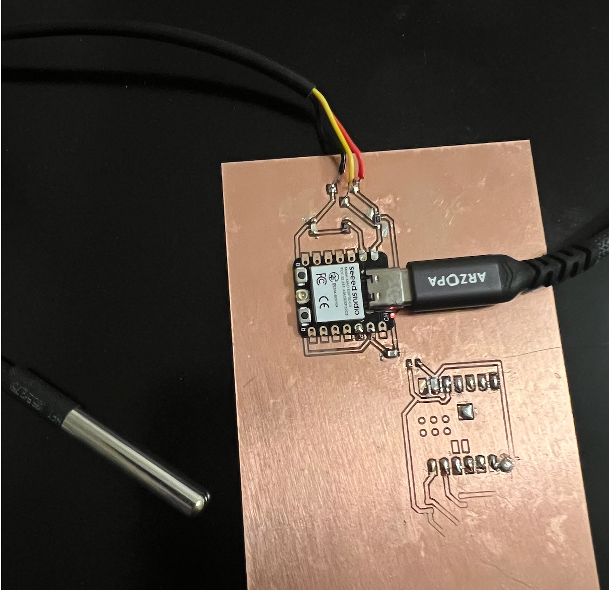
Onboard LED is lit, but the SMD LED is not - temperature probe is working
To get the SMD LED working, I used my soldering wick to remove excess solder from around the LED. It was shorting out.
Problems Encountered and Fixes
| Problem | Cause | Fix |
|---|---|---|
| Inconsistent trace depth | Board not flat, single-point Z probe | UGS Auto Leveler grid probing |
| Traces too thin on first attempt | Cut depth too shallow (0.05mm), no flatness compensation | Increased to 0.1mm + Auto Leveler |
| Solder not adhering to castellated pads | Oxidized copper + iron too hot | Scuff + IPA clean + lower iron temp (670°F) + flux |
| Bit worked loose mid-job | Collet not fully tightened | Re-tighten collet before every run |
| Wrong pin mapping in code | Generic ESP32-C3 board target selected | Changed to XIAO_ESP32C3 board target |
Source Files
- KiCad project — schematic and PCB layout
- Traces NC file
- Outline NC file
- Blink sketch
- Main.py
- config.json
Milling Settings Summary
Traces (30° V-bit, 0.1mm tip): - Cut depth: 0.1mm - Max depth: 0.1mm - Feed rate: 2 mm/s (120 mm/min) - Spindle: 10,000 RPM - Offsets: 4–8 - Stepover: 0.5
Outline (0.8mm corn end mill): - Cut depth: 0.6mm per pass - Max depth: 1.7mm (adjusted to 1.5mm for 1.4mm stock) - Feed rate: 2 mm/s
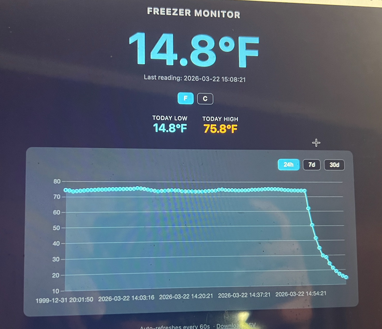
Hero Shot
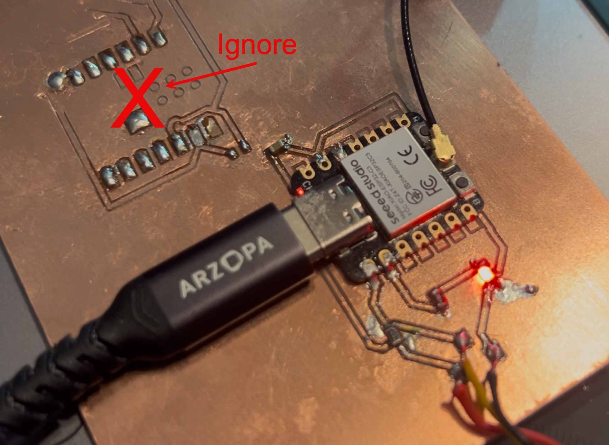 Shortly after this shot I destroyed the board. Very frustrating....from this time on until yesterday (April 11) I haven't been able to mill another board I could use for week 9 or 10. Yesterday I was able to get the settings right for consistent results. I will update in week 9 and 10.
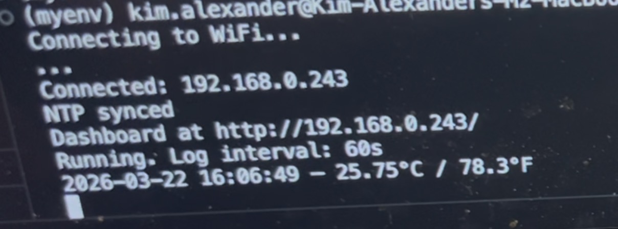 This board is capturing the temperature from the thermometer and displaying it in console and on a web server. All code was generated by Claude since I had so much trouble milling my board.