Week 8
Check List
This week's project requirements:- Characterize the design rules for your in-house PCB production process
- Document the settings for your machine.
- For milling: feeds, speeds, plunge rate, depth of cut (traces and outline) and tooling.
- For laser: all the settings effecting to the final result.
- Document the settings for your machine.
- Document the workflow for sending a PCB to a boardhouse
- Document your work on the group work page
- Reflect on what you learned on your individual page
Individual Assignment:
- Make and test an embedded microcontroller system that you designed
- Document the process
Images/Files:
- Include your original design files
- Properly compress or use a zip folder if needed
- Include hero shots of your results
Extra credit:
- Make it with another process
Group Assignment:
Resources and Helpful Links
- KiCAD
- MakeraCAM
- Carvera
- Fab Academy Tutorials
- XIAO ESP32 SeeedStudio Wiki
- MakeraCAM Workflow
- Helpful People:
- Thomas Dubick, Dr Taylor, My Group Partners Camille, Kim, and Dorian
- Thomas Dubick, Dr Taylor, My Group Partners Camille, Kim, and Dorian
Learning Outcomes
- Describe the process of tool-path generation, milling/laser engraving, stuffing, de-bugging and programming
- Demonstrate correct workflows and identify areas for improvement if required
Group Work
My Contribution to the Group Work
We started the week off with a demo from Mr Dubick. He provided us with a Front copper and an Edge cut file for a simple pcb board. As a group, we were provided a workflow and led, step by step, how to set up our files in the MakeraCAM software for our labs milling machines. We were then shown how to upload our files to the Carvera Controller software and how to safely run the Milling Machines in our lab.
After the lab demo and practice with the machines, my group got to work on our group work assignment. My group works really well, and collaboratively, and we work as a team on each step of the group work process.
We found an image of a tester that is used to determine the narrowest copper trace that mills cleanly. To be able to use this image we needed to turn it into a usable PCB file. This was an informative process for me as I learned how to import a png into MakerCAM and trace it within MakerCAM to use it for a project. We created a few more testers to test different settings on the lab machines as well as worked through the process, as a group, to pretend to buy a board from a boardhouse.
-
My Contributions to this week:
- I traced the image of the trace width tester in MakeraCAM to create a usable file for milling.
- I created the toolpaths for the trace width tester in MakeraCAM using the 0.8mm corn bit.
- I worked with Camile and Kim to mill the tester boards on the Carvera CNC machines in our lab.
- I tested the trace width tester we created on the milling machines and documented the results.
- I followed along while, as a group, we walked through the process of sending a board to a boardhouse.
For a more in depth look at my groups week 8 assignment, see my groups Week 8 page.
Introduction
I really enjoyed taking the time this week to work with KiCAD, the MakeraCAM software, and running the Carvera CNC machines to make boards. I had a little bit of practice with the milling machines earlier this year when they were first installed, but I haven't had a chance to really sit down and use them since. I feel a lot more confident with the machines and the software then I did prior to this week.
Setting Up my KiCAD
Adding FabLab Library
One of the first things I had to do this week was set up my KiCAD on my personal computer and my work computer to have all of necesary and the correct libraries. I needed to ensure that I had the proper Fab Lab libraries installed on my home computer, and necessary libraries for the boards I want to use. On the computers at work, we practiced adding symbol and footprint libraries directly into KiCAD from files. Howerver at home, after some research, I learned of a quicker and easier method for installing the FabLab libraries.
On the FabAcademy Tutorials site, I found the KiCAD FabLib set up process.
According to the site,
"FabLib makes it easy to produce PCBs at a standard Fab Lab. There are more than 2k Fab Labs in the world and many of them will have electronics components from the official Fab Inventory. The goal of FabLib is to have 1:1 mapping with the parts from the Fab Inventory which reduces friction when learning electronics and boosts confidence when prototyping rapidly at a Fab Lab."
I followed the tutorial on the site which started with accessin the Plugin and Content Manager tab in KiCAD.
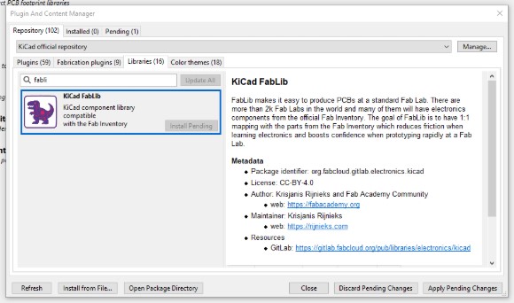
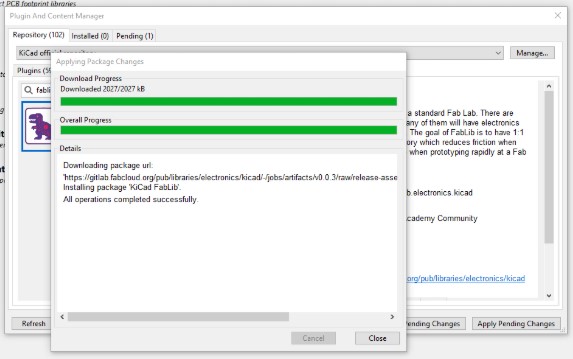
Within this tab, I searched for the KiCAD FabLib library and began to intall the library.
Adding My Board Libraries
After installing the FabLab libraries, I next needed to make sure I had the necessary footprints and symbols for the different boards I plan to use and try. I knew I had one hand an ESP32-C3, an ESP32-C6, an RP2040, and an ESP32-S3. Since I planned to try this different boards as I work to finalize my board for my final project, I figured it would make sense to install all the libraries on my home computer.
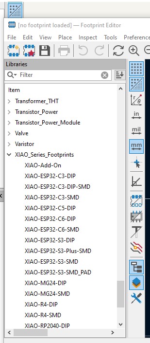
I started by navigating to the SeeedStudio Wiki page and checked the files for each of my boards. I noticed that XIAO had a standard footprint and symbol file for all of the boards, so I only needed to download each of those once to cover all of the boards I planned to use.
Fun tip, use Control-F to seach the page for Footprint to quickly and easily find the PCB Design Libraries.
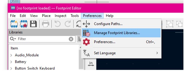
After downloading the files, I opened my KiCAD and navigated to hte Footprint Editor.
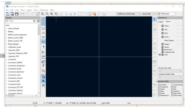
Once in the Footprint Editor, I navigated to Preferences > Manage Footprint Libraries and then added the extractred foorprint folder I had just downloaded.
After installing the footprint library, I doublw checked in the Libraries list that I could now see the XIAO boards.
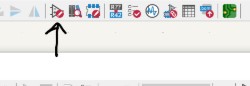
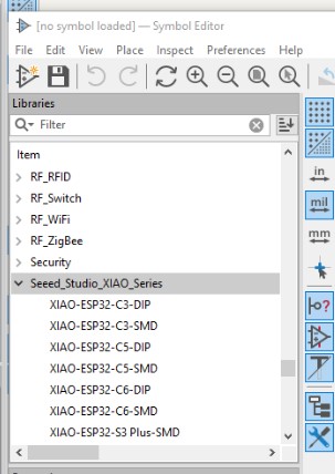
Next, I needed to install the symbols for the XIAO boards. The process is very similar to adding a footprint. I navigated to the Symbol Editor.
Then navigated to File > Add Library > Global > Find and Add. From the menu I looked for my .kicad_sym file and added it. Just like with my footprint, I doubled checked the Libraries to ensure I could see the Xiao Series symbols.
Using MakeraCAM
As a lab, Mr Dubick provided us all with a sample project file and walked us through a step by step lesson to set up a basic board and prepare it for milling. In the lesson we learned how to move and select objects, set up toolpaths, we learned which bits we have in our machines, how to calculate toolpaths, how to simulate our board, and finally how to export the files as .nc file types. When I got home, I downloaded the free 15 day trial of the MakeraCAM software so I could conmtinue to practice the process at home.
Milling my Board
MakeraCAM
I followed the steps given in our labs workflow to set up my board for milling in MakeraCAM and then I sent it to be milled on the Carvera CNC machine in our lab. The process I followed for preparing this board in MakeraCAM is as follows:
- I downloaded the Front Copper and the Edge Cut Gerber files from Mr Dubick's Google Drive. Typically though, I would need to export the files from KiCAD.
- I opened MakeraCam and set up a new project.
- I set the stock on the left hand size to match the size of the board I was milling. For this project the stock settings were:
- Material = PCB
- Length = 120mm
- Width = 101mm
- Height = 1.7mm
- I imported the Gerber files into MakeraCAM.
- I drag selected all the parts in my design and used the keyboard command M to open the move menu. In our lab we always set the Anchor to the lower left corner and set both the X and Y location to 6.
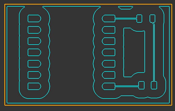
- I next set the boundary by selecting everything on the Front Copper and Edge layers, then deselecting the outtermost line on the outline. I had to zoom in close to see that thier are actually two lines on the outline, and I needed to make sure I only kept the inner line selected.
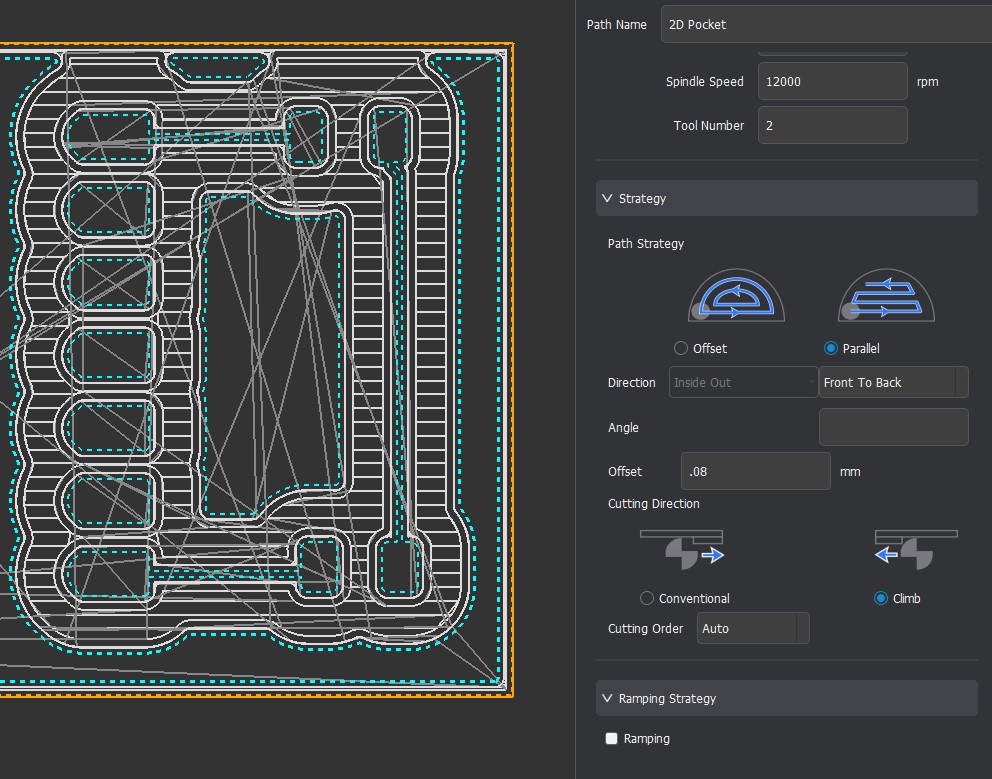
- With these lines now selected I created a 2D Pocket Toolpath. I used the following settings in my 2D Pocket.

- Cutting Start Depth = 0.0mm
- Cutting End Depth = 0.05mm
- 0.8mm Corn Bit - This one needs to be on top of the list of bits
- 0.2mm 30 degree Engraving Bit
- Path Strategy = Parallel
- With these settings I clicked calculate and I was ready to move on to the toolpath for the board outline.
- I started to set up the next toolpath by hiding all of the layers except for the Edge Cuts layer.
- I once again zoomed in and deselected the outermost line on the outline.
- I then set up a 2D Contour Toolpath with the following settings:
- Cutting Start Depth = 0.0mm
- Cutting End Depth = 1.7mm - the thickness of the board
- 0.8mm Corn Bit - This one needs to be on top of the list of bits
- Tabs = 3 - 4 tabs along the edge of the board
- Path Strategy = Outside
- I clicked calculate and now I was ready to simulate and export my board!
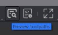
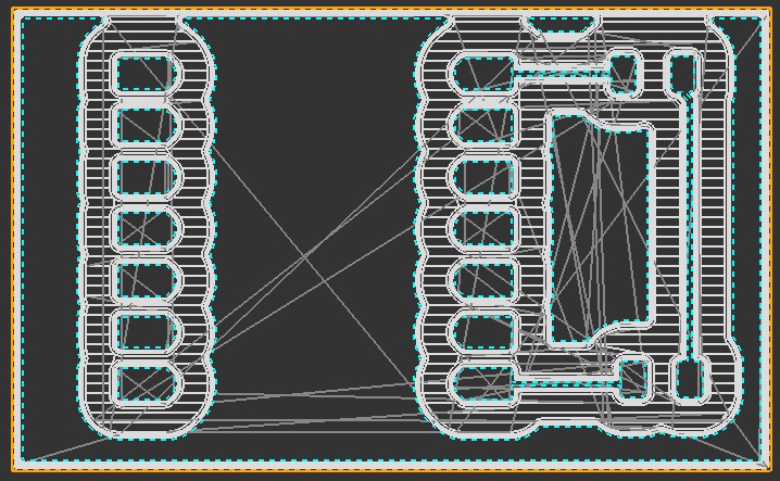
In the popup I selected all of my toolpaths and then clicked on Preview button to watch my simulation. In the simulation menu you can turn on and off a few different options, like the bit and board, to help you see the simulation better.
I was happy with the simulation so I exported the files as .nc files which is the file type needed to run the Carvera CNC machines in our lab.
Carvera CNC
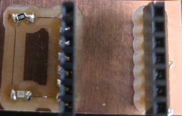
The first board I milled was unsuccessful. As you can see in the image, the milling machine did not mill all the way through the copper.
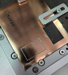
Even though it didn't mill well, I still planned to attempt to use the board as I did not have time to mill another one that day at work. later in the day, it was also brought to my attention by another teacher in my lab, that the traces were very thin. They found that other boards made with the same small trace size of 0.2mm, would have thier traces easily scratch off.
It was suggested to update the design and use 0.5mm for the traces for better success, instead of the 0.2mm size traces given to us in the premade file.
I didn't have time that day to make the corrections or mill another board, so I attempted to use the board. At this point, our lab was going to be closed for our school's Spring Break for the next 9 days. At home I ran a continuity test on the board, but unfortunately it was so poorly milled that nearly all of the lines were connected.
Redesigning my Board
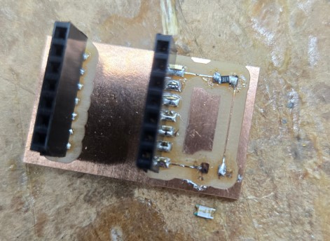
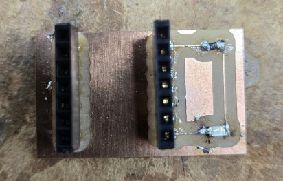
Since I was unable to use the board I had and unable to mill until the lab was reopened after break, I decided to update the board design with the larger traces as suggested. For the test board, we were only given the edge cut and the front copper files to use in our demo and not the actual KiCAD project file. To update the board required me to remake it, so I rebuilt the board, from scratch, in KiCAD using the poorly milled one I had on hand as a reference. Since I was building the new board from scratch I had some freedom to make updates and changes to the design, overall I kept the layout identical but did increase the trace width to 0.5mm.
Milling my Board Again
Once we were back in the lab, I sent my redesigned board to be milled. In Carvera CNC I needed to prepare my board for milling. The machine was showing as disconnected as it hadn't been used and was powered off for spring break so I powered on and connected the machine via USB connection on COM3. It took a moment but it eventually connected and I was able to upload my .nc files. I tucked my board against the edge spacers and secured my copper to the bed using the metal clips.
In the Carvera CNC software I used the following settings in the Config and Run menu.
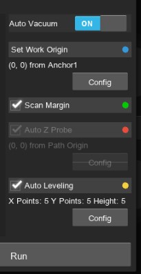
- Auto Vacuum = On
- Set Work Origin = 0,0 from Anchor 1
- Scan Margin = checked
- Auto Leveling = Checked for 5 points in the X, Y, and Z axis.
I hit run and watched the machine do its probing to ensure it was going to mill where I expected it to. Once it all looked good I let it run and watched the milling process.
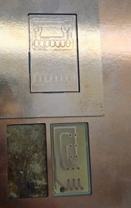
Unfortunately, there was another issue with the milling. I tried again, and after a few more unsuccessful attempts with mine and other peoples boards, it was discovered that there was a small chip in the bit that was being used.
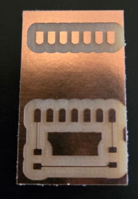
After the bit was changed out for a fresh one, I was finally able to mill my board successfully. Since it was now technically week 9, I also milled my week 9 board at the same time.
Soldering my New Board
I did not enjoy surface mount soldering, but I was able to do it. I started by adding a bit of solder to each pad, this part was very satisfying as the solder freely and smoothly flowed over each pad.
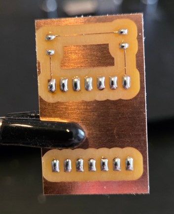
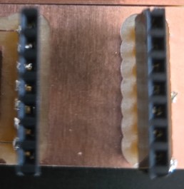
We were given strips of 90 degree female pin headers to use.
Since my pads were shorter than the legs of the headers I had to trim the feet back on the headers so that they didn't stick past pads and onto the copper or other traces.
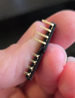
I carefully held a cut strip of 7 header pins onto the soldered pads and heated up one pad to set the pins in place. After locking the header pins in place, I then finished soldering the rest of the headers. I did this for both sides on my board where my ESP32-C6 would sit.
I then pulled out a 330 ohm surface mount resistor and a red surface mount led and I did my best to solder them in place. I was working with what I had, and used the 0805 sized components from the book we were given, however our sample board was designed to use 1206 sized components. The 0805s were a tiny bit short compared to the distance between the leads, but I compromised by flooding some more solder to reach. I honestly did not do a great job at surface mount soldering the resistor. You can clearly see that it is crooked.

They were so small and I really struggled with holding them still while trying to solder them in place. I lost at least two of them on my carpet while trying to solder this board.
Finally, I soldered the red LED, which went a lot smoother than the resistor.
Testing my New Board
I plugged in my ESP32C6 and ran the basic led blinking code to the onboard led to ensure that everything was working on the ESP. After checking the ESP was in working condition I updated the code to blink the surface mounted led, and nothing happened.
I got out my multimeter and checked for any issues with the traces and they were fine, I was able to read the 330 ohm resistor, and I was able to light up my red LED using the meter. It was at that point I realized, I soldered the red LED on backwards. I also realized, the LED was going to the 5v pin and was before the resistor because I put them in the wrong spots. I actually probably saved the red led from being blown out by putting it on backwards.
Fixing my Board
I finally had a chance to fix my board! I started by desoldering the LED and the Resistor. In the process of desoldering the components I lost both pieces, and I burned off the pad where the LED sits.
I grabbed new components to replace thw two I lost while desoldering and did what I could to fix it. Their was a non-zero chance I would need to remill the board, but I wanted to at least try and make it work if I could. I used the same value resistor as the first one, but this time I grabbed a nice, bright, Red LED. I was more careful this time with soldering the components and ensured that I soldered the resitor on top and the LED on the bottom. I also made sure to notate where the blue indicator was on the LED to ensure I soldered it on correctly this time.
I plugged in my ESP32 and connected it to the computer and ran the example blink code for the onboard LED. This time, the LED blinked as expected! Woohoo!
Week 8 Files
In my repo is a zip folder containing files for my week 8.
What files are inside my Folder:
My files for the test board we were given
My files for my updated version of the test board
My Arduino code for the blinking LED test
Download My Week 8 Project Files Zip Folder