Week 6: Electronics Design
Assignments
Group assignment:
Characterize the design rules for your in-house PCB production process: document the settings for your machine.
Document the workflow for sending a PCB to a boardhouse
Document your work to the group work page and reflect on your individual page what you learned
Individual assignment:
Make and test a microcontroller development board that you designed
Group Assignment Reflection
This week's group assignment focuses on getting familiar with commonly used electronic measurement tools in the FabLab. These include the multimeter, logic analyzer, and oscilloscope. Understanding how to use these tools effectively is crucial for debugging and testing electronic circuits.
The Oscilloscope:
The oscilloscope is used to capture and visualize electrical signals over time. It helps in analyzing signal behavior, identifying noise, and debugging timing issues in circuits.Oscilloscope for visualizing and analyzing signals (I2C CLK measured at 44 kHz, different oscilloscope models tested: 53M, 13M, 26M).
Key Functions of the Multimeter:
The multimeter is a versatile tool used to measure various electrical quantities, including voltage, current, and resistance. It is a fundamental instrument in electrical engineering and electronics for troubleshooting and circuit analysis.
Voltmeter/ Voltage measurement: Checking power supply and circuit voltages. Ammeter/ Current measurement: Measuring current flow in a circuit. Resistance measurement: Testing resistance of components, basically resistors. Conductive checking: Checks if two testing point is connected (often expressed with a beep sound).
Workflow
Individual assignment:
This week, I learned how to use the PCB design software and the workflow of sending a PCB to a boardhouse. I was try to learn EasyEDA and KiCAD to design a microcontroller development board.
Circuit Simulation
Before forming PCB, I built a simulation in Wokwi which is an online electronics simulator.
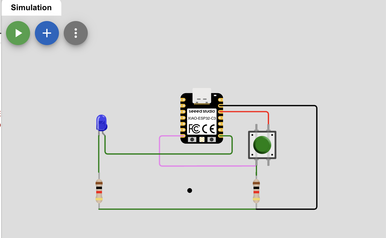
The code for the circuit simulation is as follows:
                    void setup() {
                      Serial.begin(115200);
                      pinMode(D6, INPUT);
                      pinMode(D7, OUTPUT);
                    }

                    void loop() {
                      digitalWrite(D7, LOW);
                      Serial.println(digitalRead(D6));
                      if(digitalRead(D6) == HIGH){
                        digitalWrite(D7, HIGH);
                      }else{
                        digitalWrite(D7, LOW);
                      }
                    }
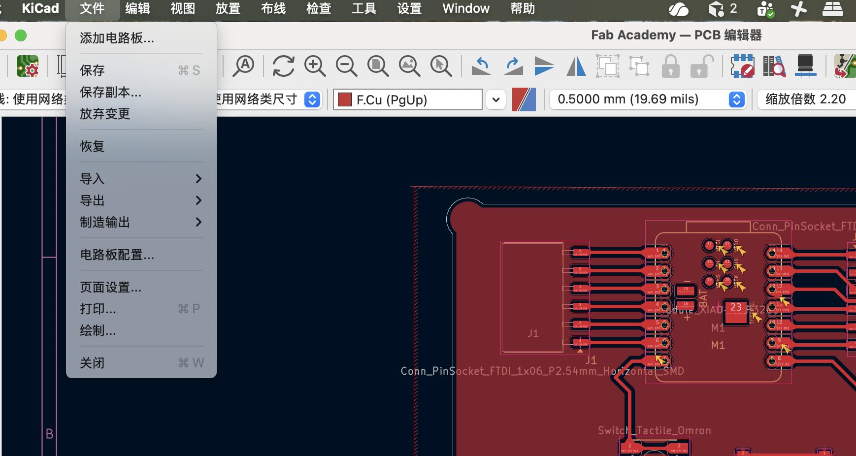
How to use Kidcad to design a PCB
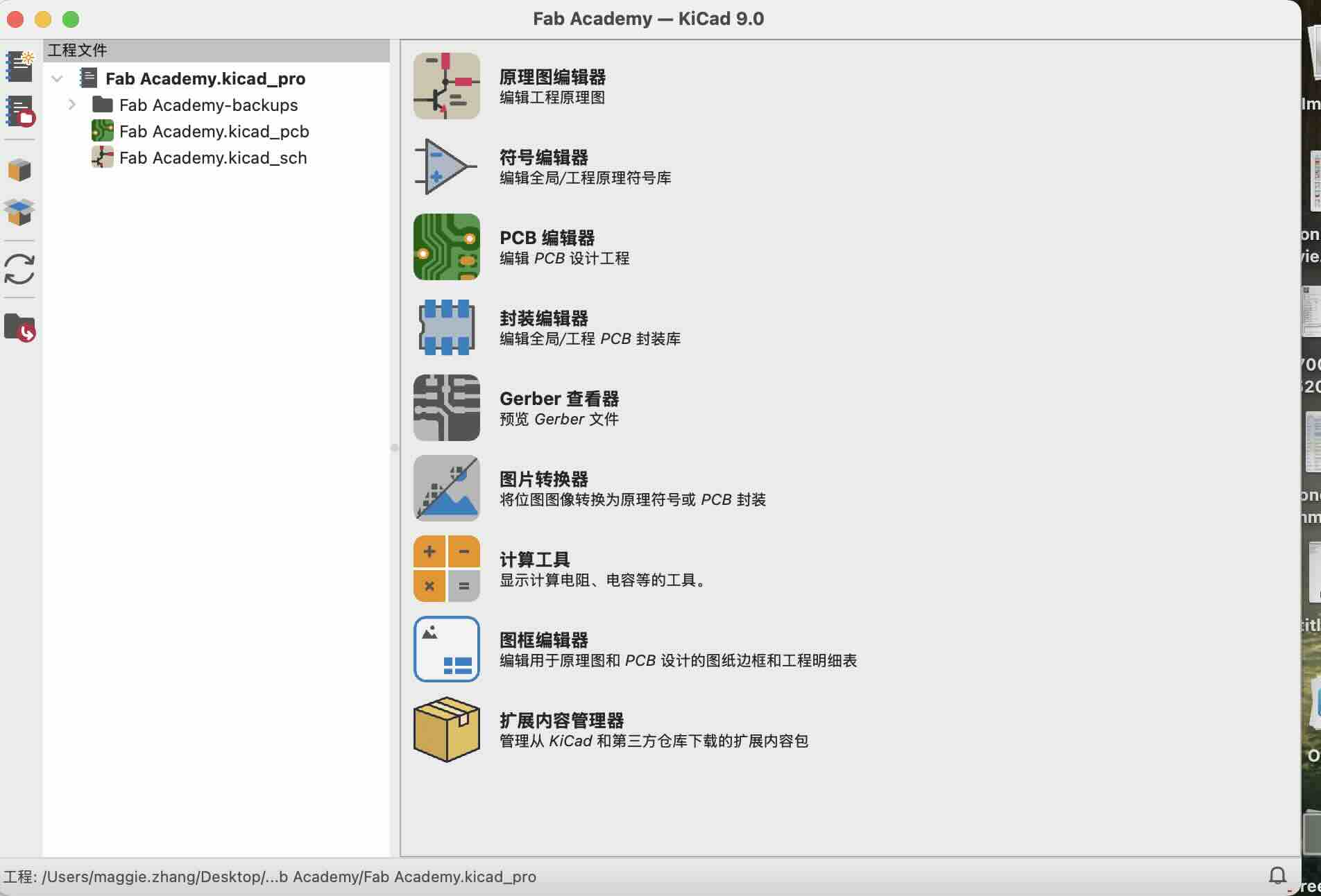
Step1: Creat project and download the library
First, Download the library and unzip it. The library is provided by Fab Academy. Then open the library and click the "New" button to create a new project.
Then, add the components you need to the project. You can search for the components you need in the library.
Finally, click the "Save" button to save the project.
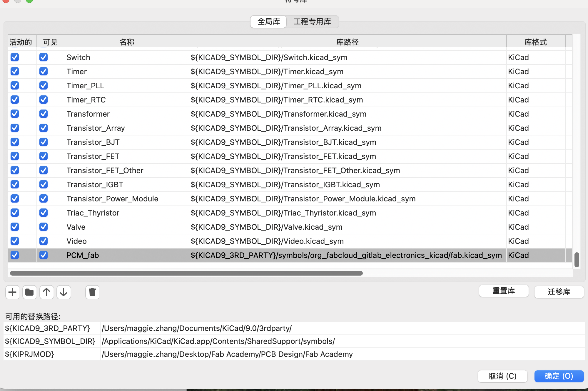
Before adding electronic components to your schematic, the libraries of the components from fabacademy needs to be installed first. Go to the "Manage Symbol Libraries" and add the library we just downloaded.
Step2: Drawing the schematic file
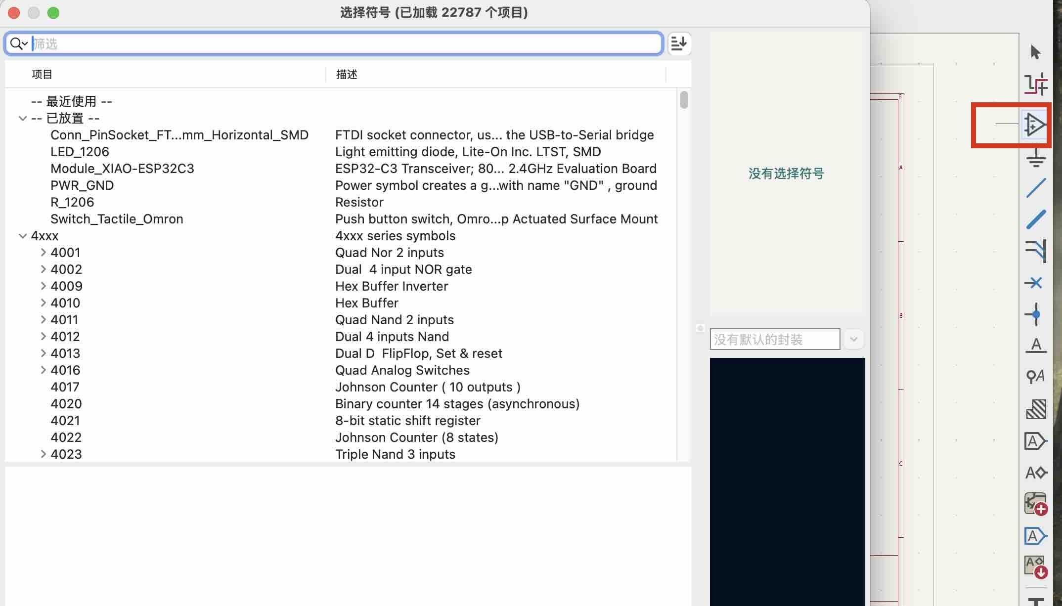
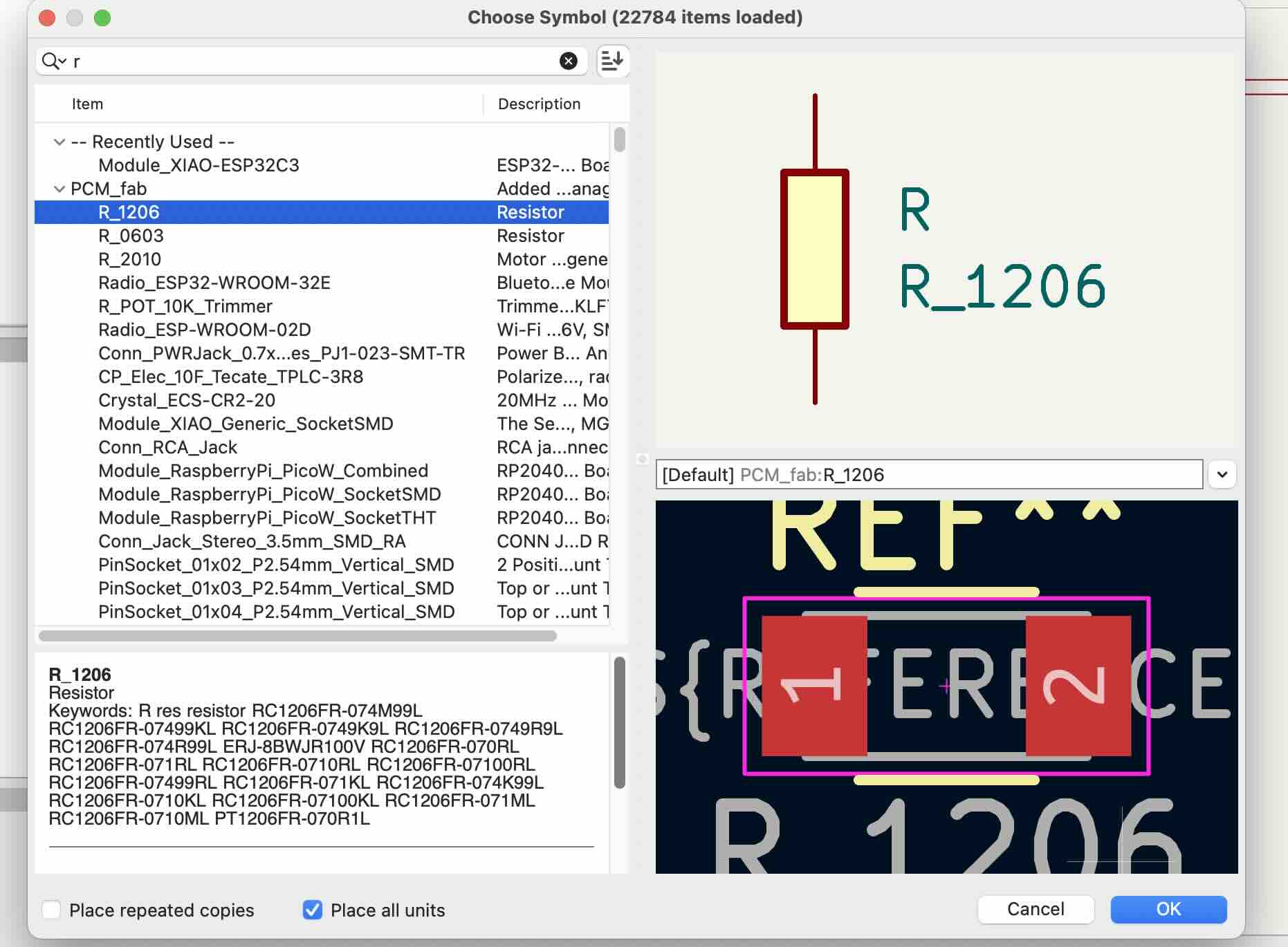
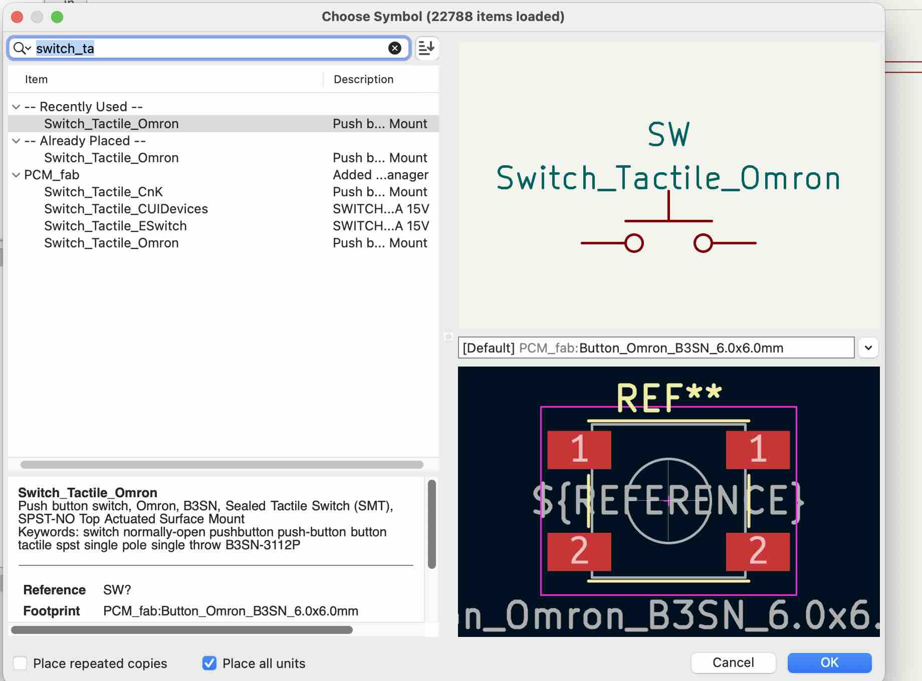
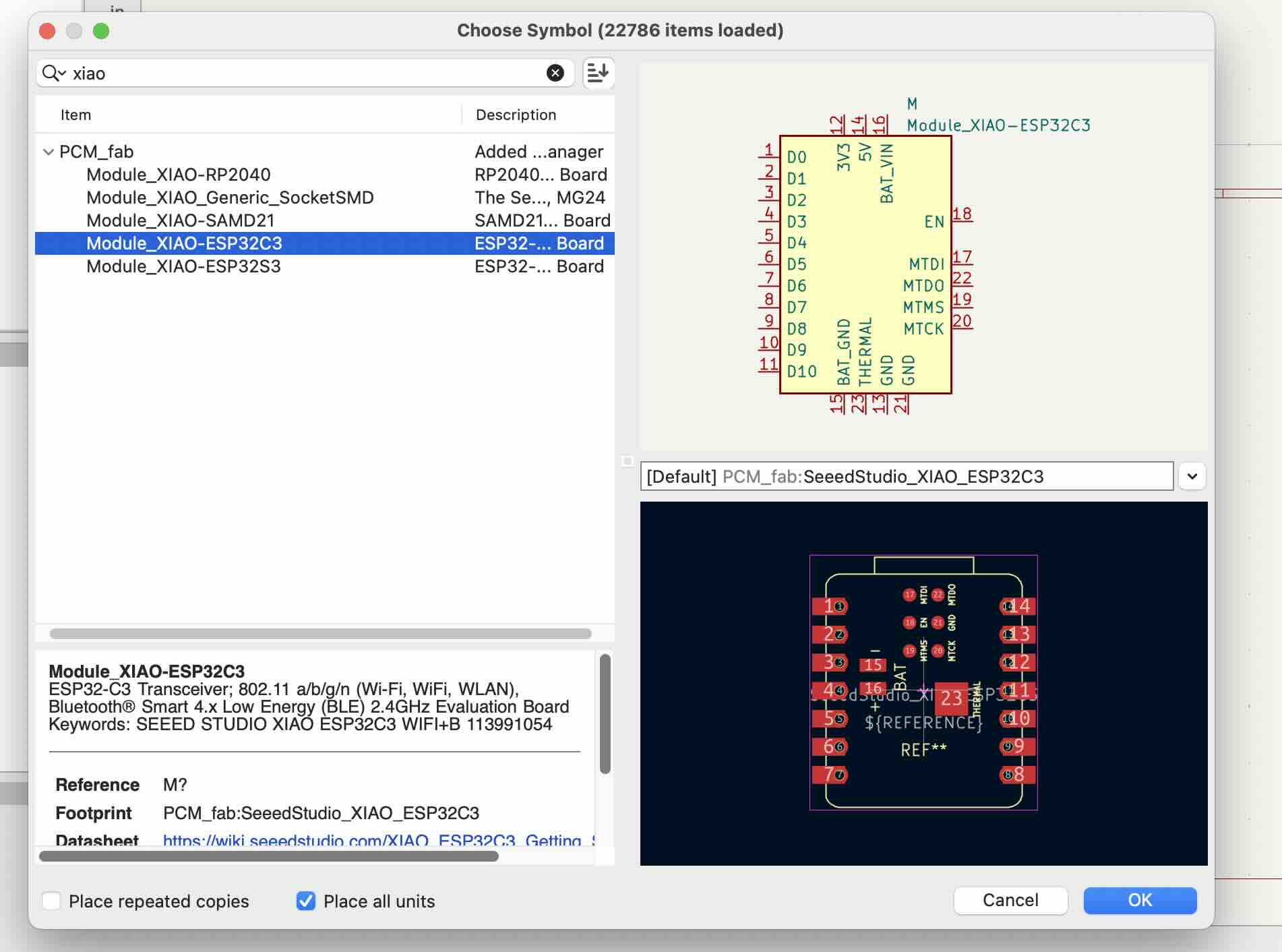
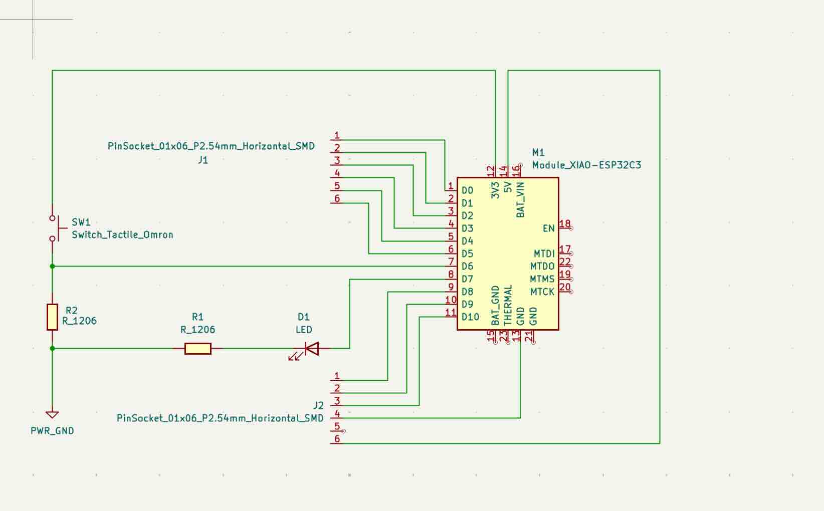
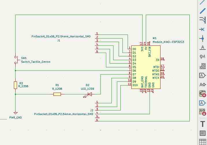
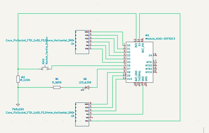
After creating the project, you can start to draw the schematic file by searching from Choose Symbol. The components library is as follows(The Led and pinsocket are the final version that I used):
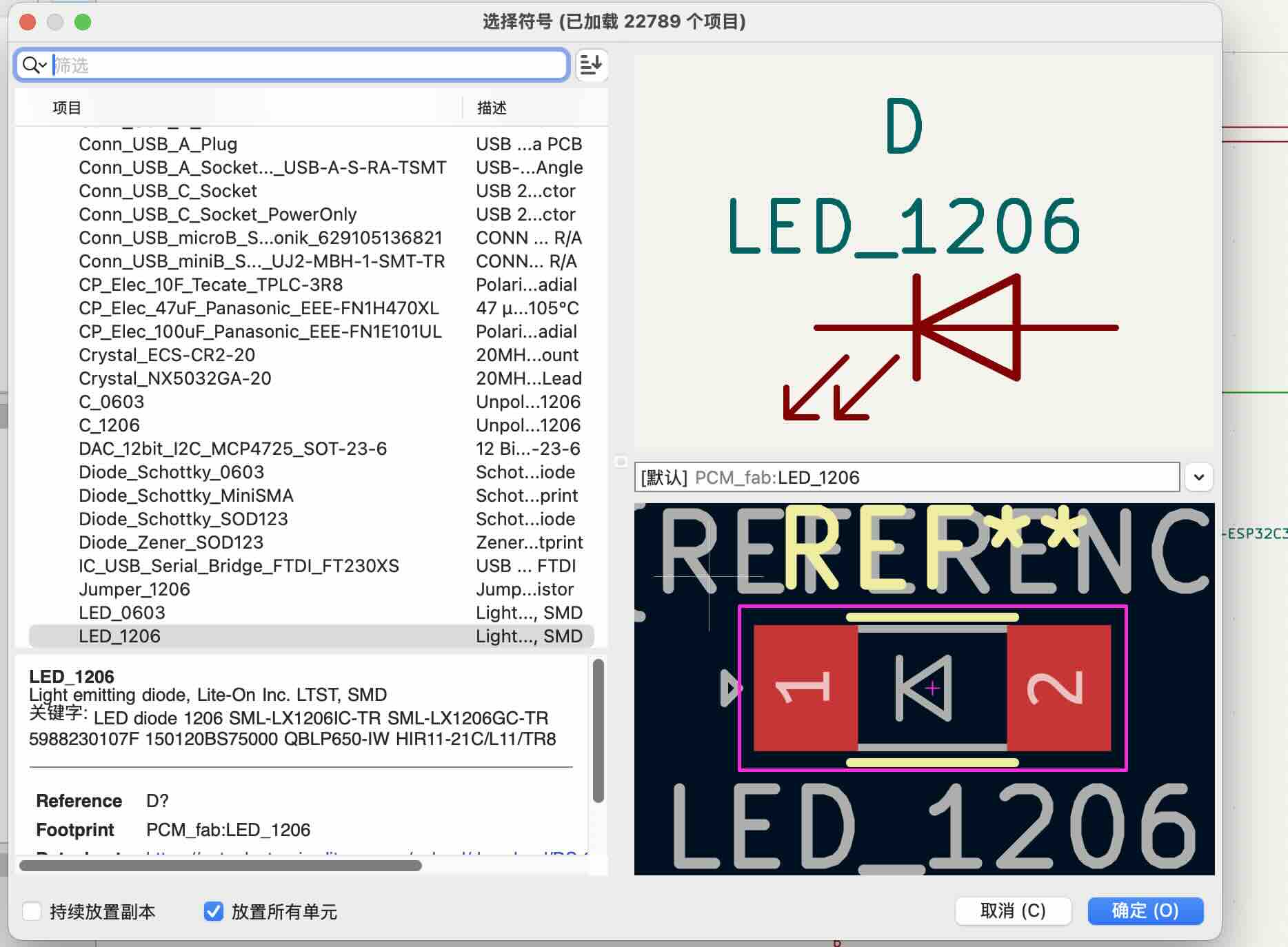
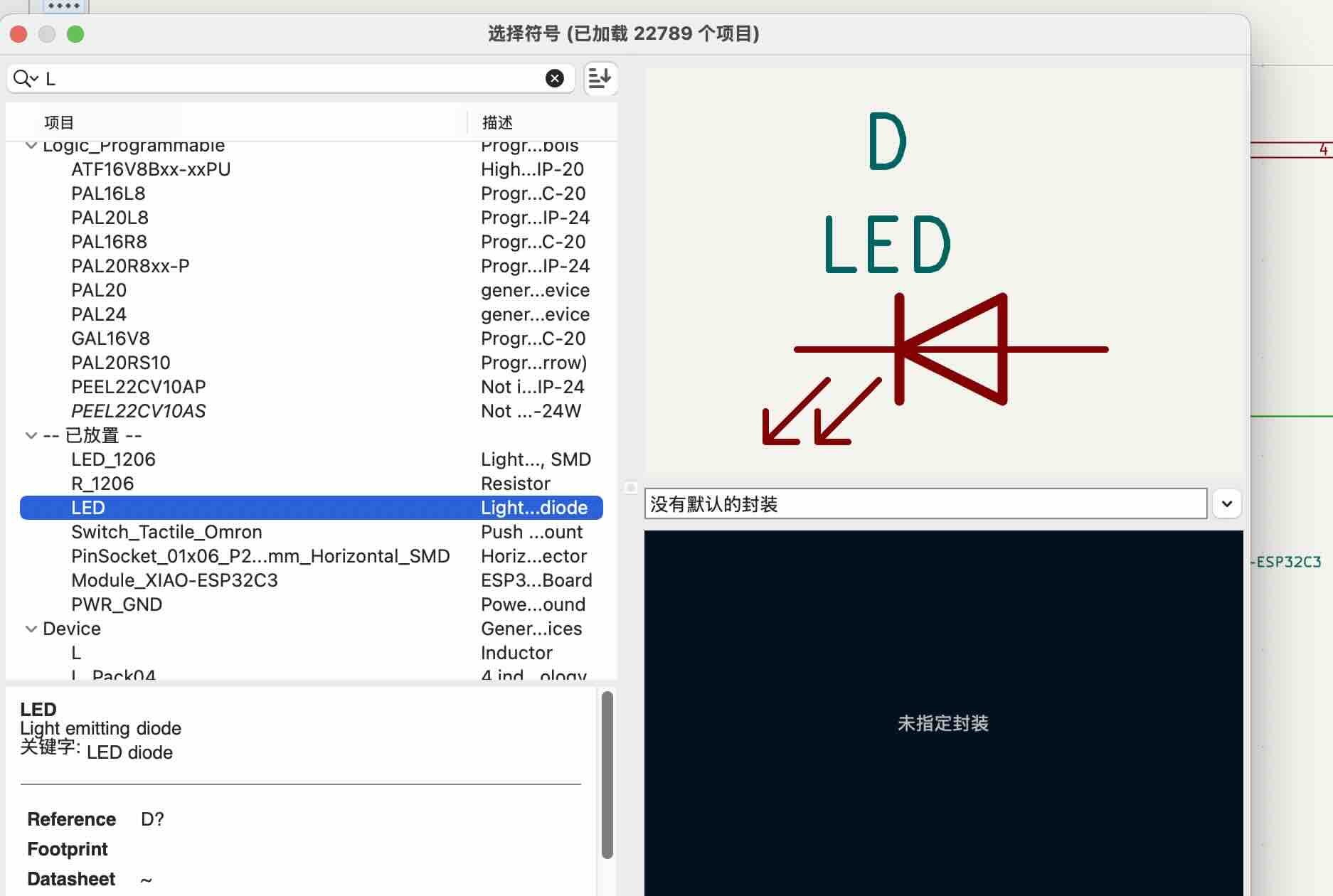
Design a simple circuit with pull-down resistor to switch for prevent from short circuit and burn out the circuit. But I found the circuit is not working after I click the "update Schematic to PCB", I can see the PCB design, but there is one component LED is not shown, and schematic shows"no default footprint", and after update PCB, there is no LED at all,so I need to check the circuit again. I changed the led to LED_1206 that setting shows {default PCB_ fab:LED_1206}.
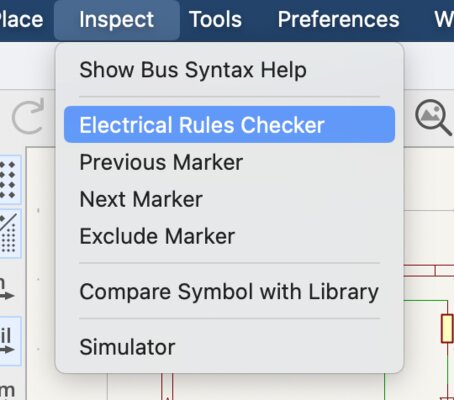
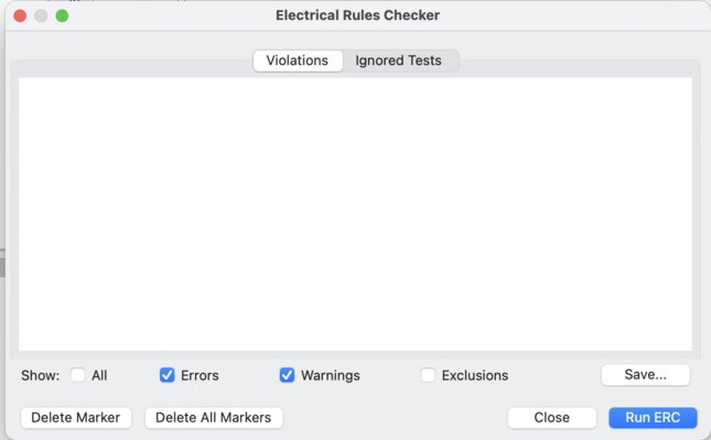
That means after writing the components according to my circuit design, I should run the Electral Rules Checker to ensure there were no logical errors or disconnected pins.
Click Inspect -> Electrical Rules Checker and Click Run ERC.
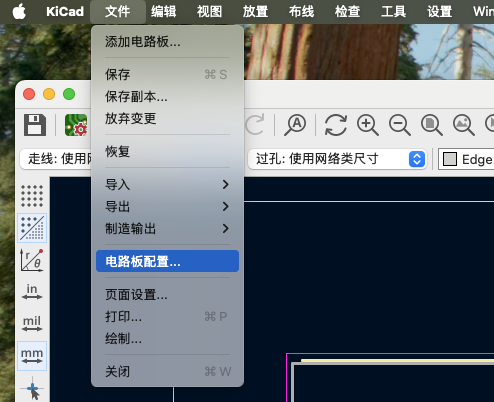
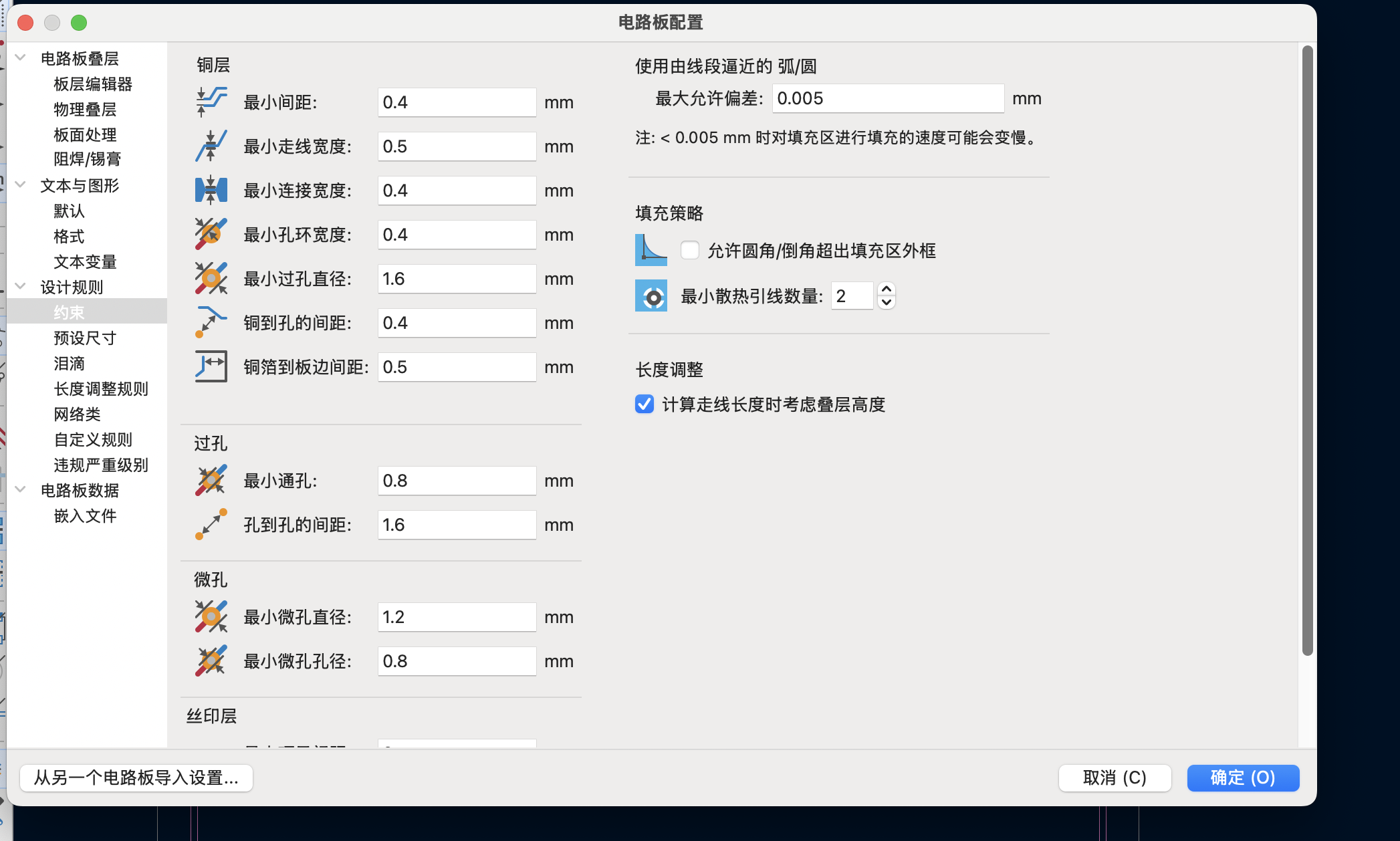
The next step is to adjust the PCB design rules. Click files, under board settings.
Click "Board Settings" to adjust the PCB design rules.
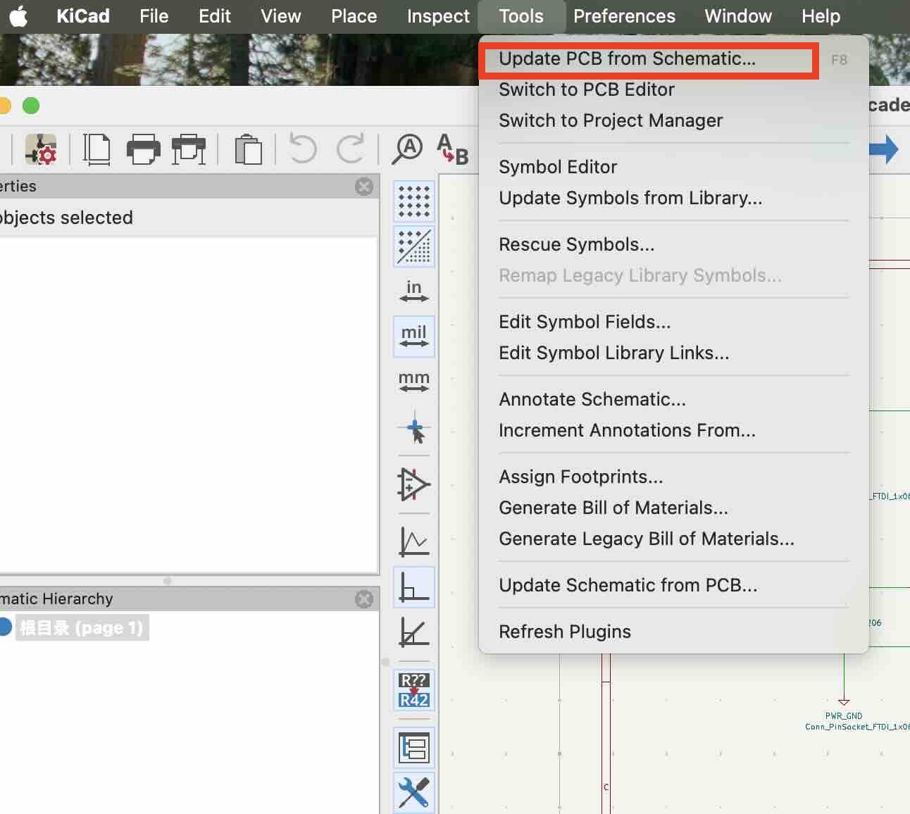
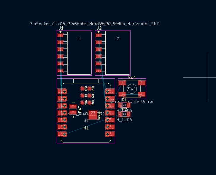
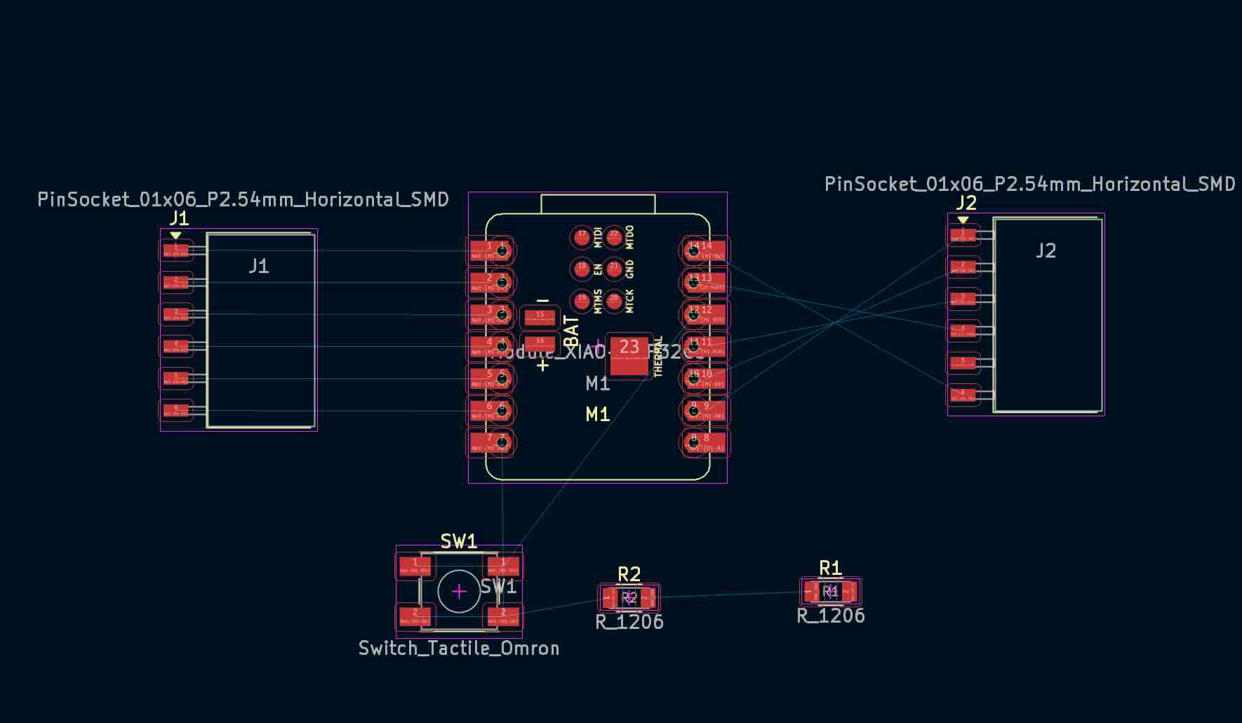
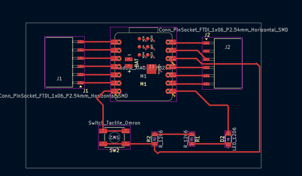
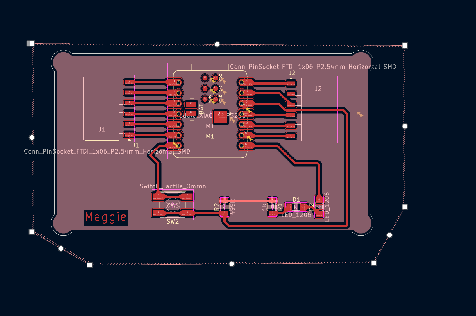
After drawing the schematic file, you can start to draw the PCB layout.
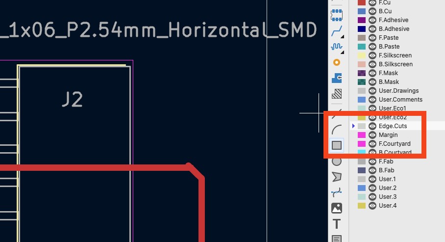
Afer finishing the trace layer, change to cut layer (Choose Cut Edge)and draw the boarder of the circuit board. But I found the circuit routes are so wired, so maybe I need to adjust the PCB design rules.
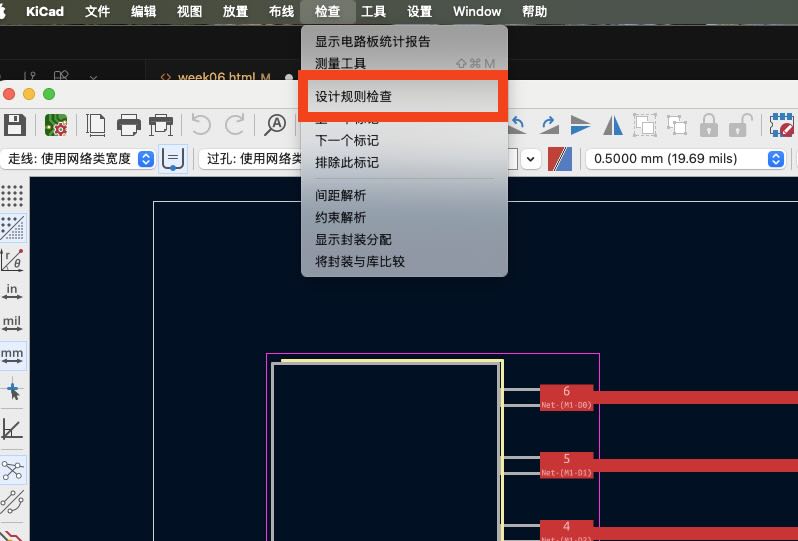
Before export the layout files, you can use the DCR tool to check the design of circuit board is legal or not.
If shows no error, but only warnnings,you can export the layout files.
I also do the simulation fo the circit board,but I realize the pinsocket is not connect in the right way, so I back to the schematic file and adjust the circuit again.
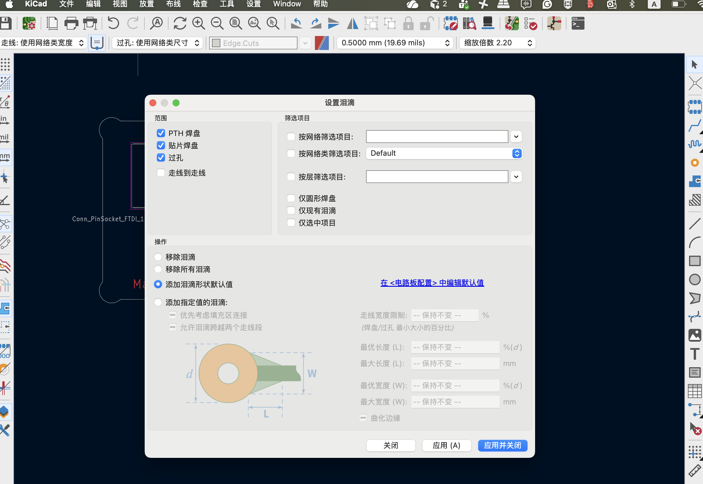
Step3: Adding Teardrops
Select "Edit"->"Add TearDrops" from the top menu.
In the "TearDrop Settings" windows, configure teardrop parameters which is suitable for CNC milling.The parameters are as follows:
Click "Apply" to observe the effect
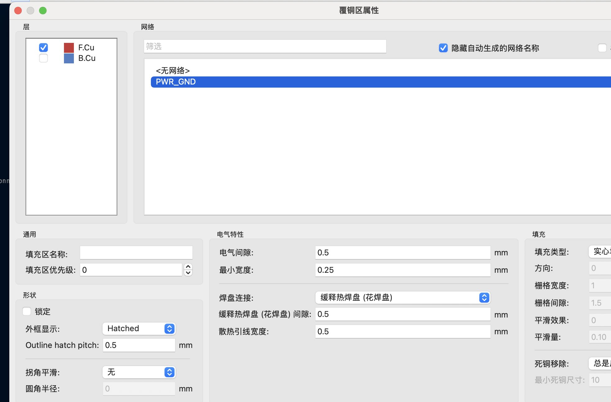
Step4: Adding Copper Fill
Select F.Cu layer on the left side of the tool bar, select the "Draw Fill Zone" on the right and choose the filling area. The properties windows will appear and select GND in the network. Select the copper fill area. In this case, choose the entire PCB board as the filling area. Press shortcut Key 'b' or click menu "Edit"->"Fill All Zones" Ensure the copper fill area maintains sufficient distance from signal lines
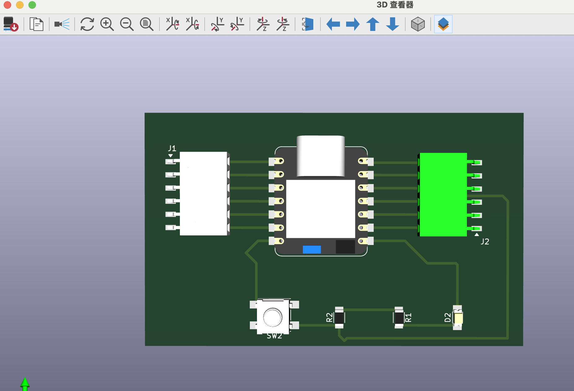
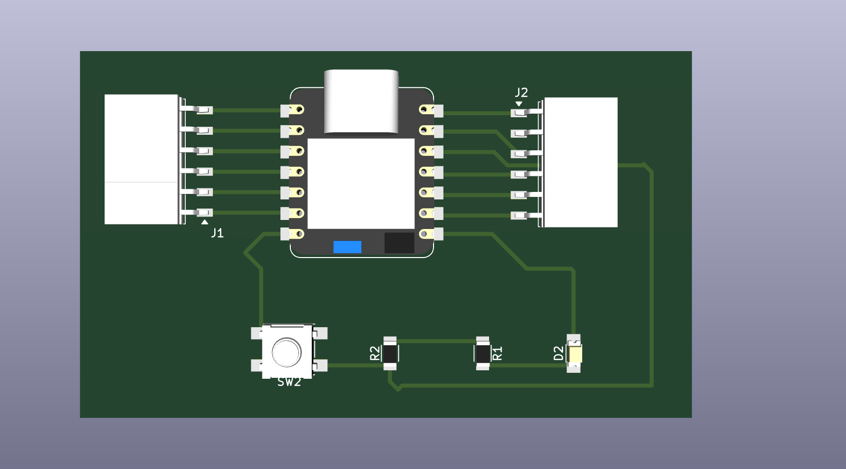
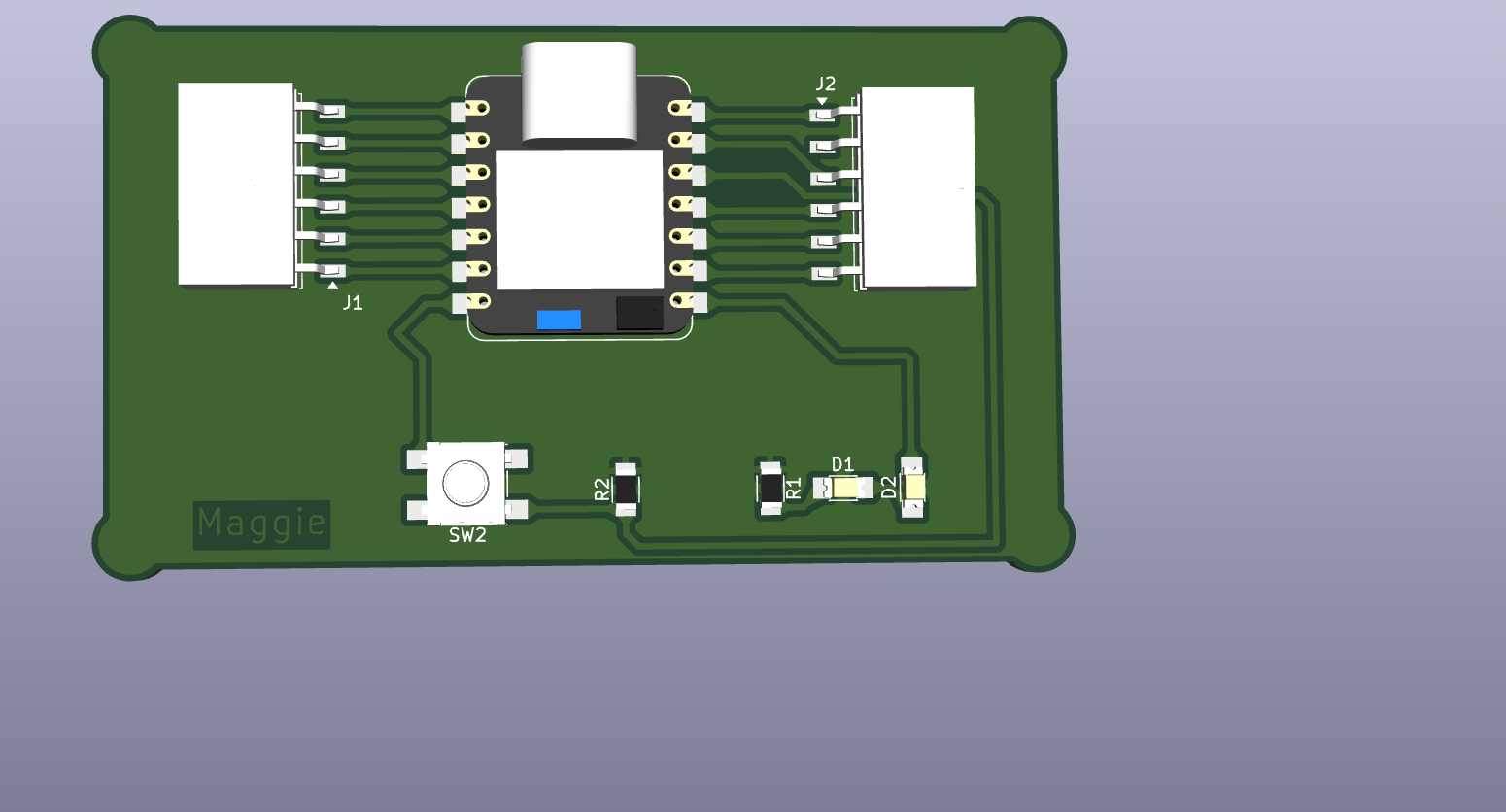
Veiw the 3D model of the PCB board, if everything is ok, At last export the PCB board to Gerber file.
File sharing
Here is the link about this assignment which included:
Fab Academy-Edge_Cuts.gbr — Edge_Cuts layer (Gerber export).
Fab Academy-F_Cu.gbr — F_Cu layer (Gerber export).