individual assignment
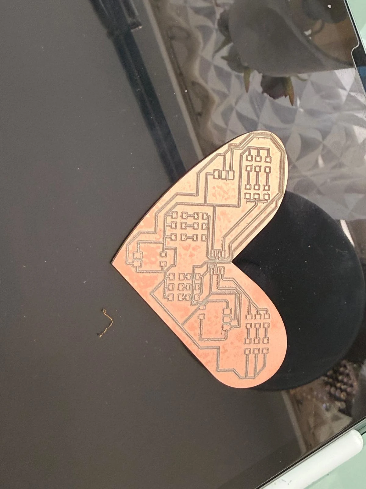
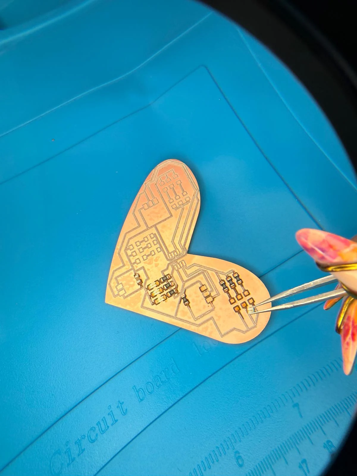
This week I cut 2 boards. One from the design week & a slightly advanced different version for my final project.
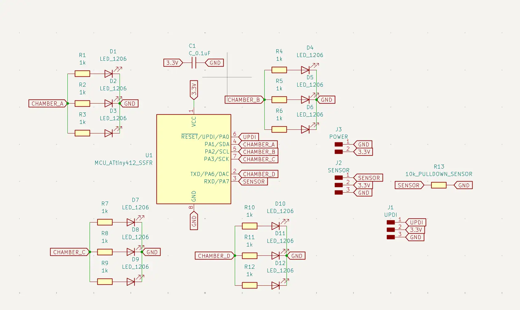
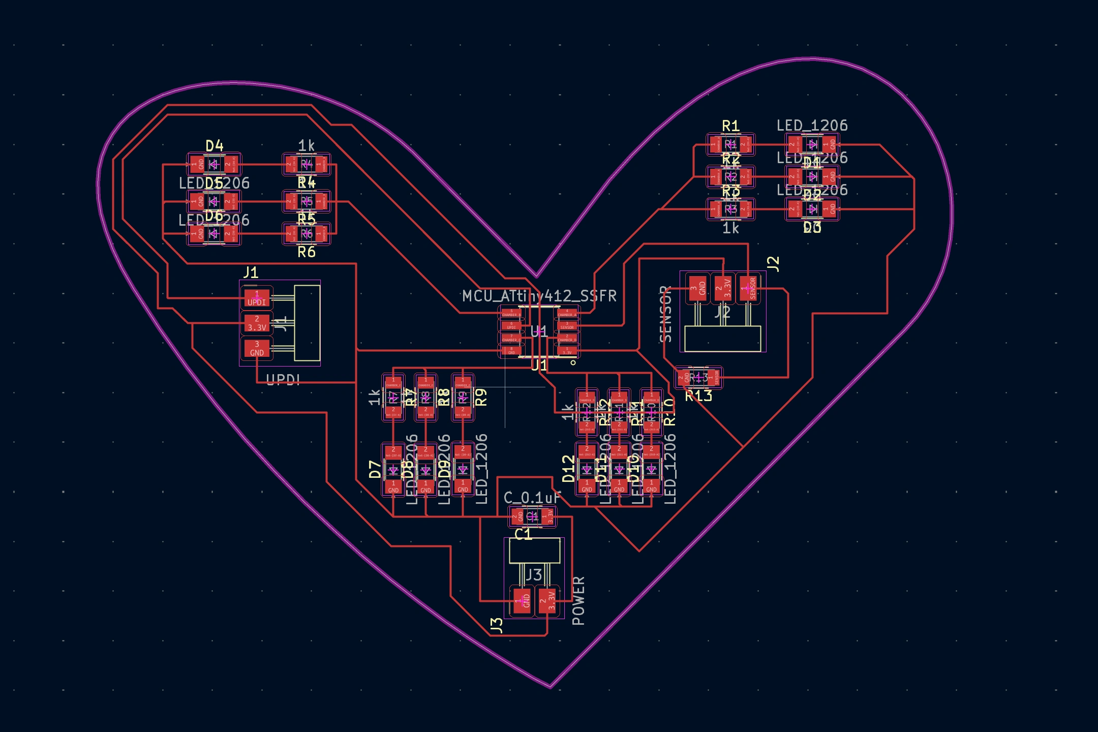
1. basic heart shaped LED board with pulse sensor, LEDs & an ATTiny microcontroller.
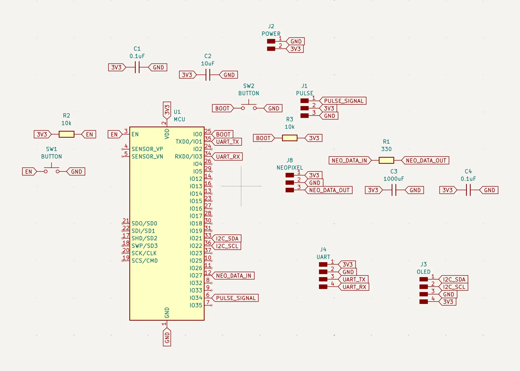
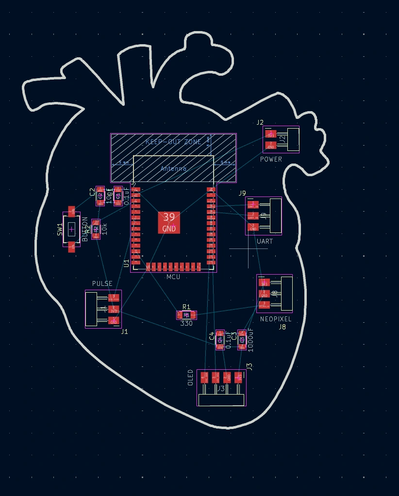
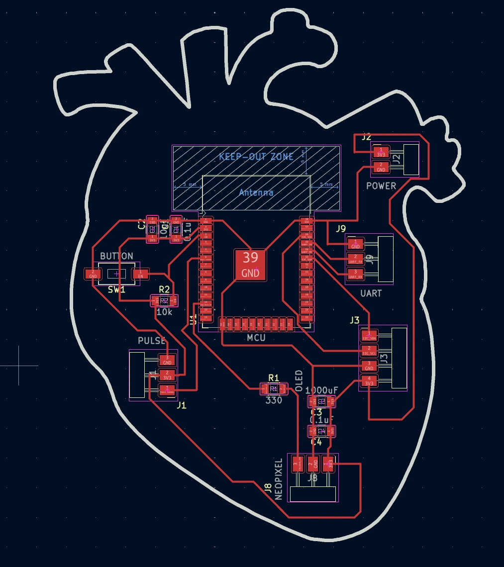
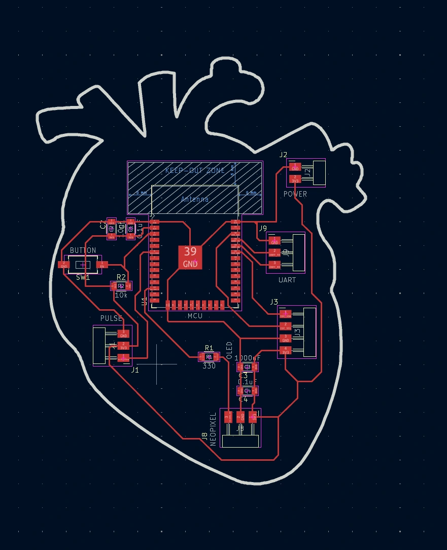
2. Real heart shaped ESP32 board with pulse sensor, neopixel & oled.
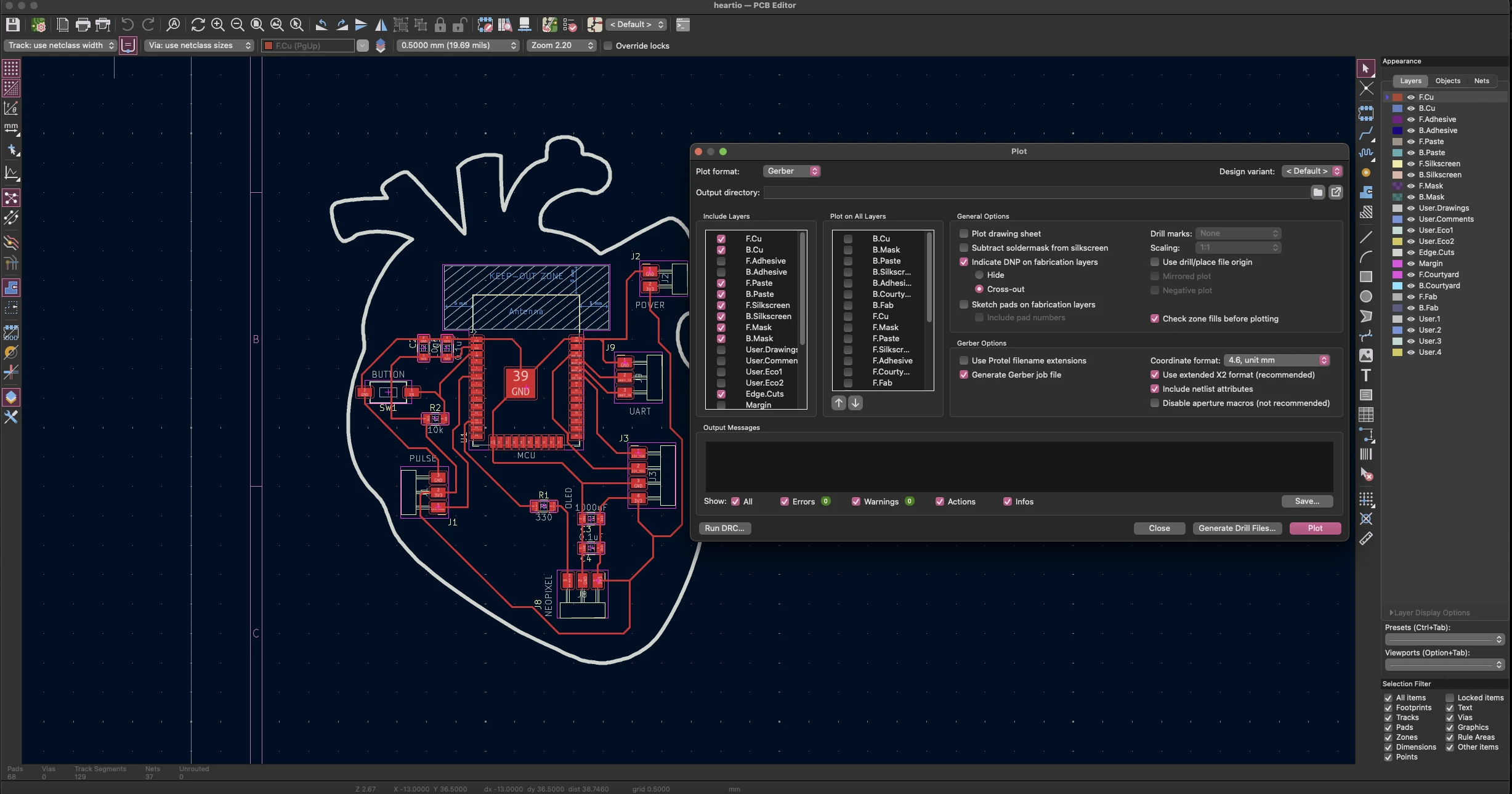
On KiCad, create the wiring connections & export the necessary files. The traces should be in the layer F.Cu and the outline should be in the layer Edge.Cuts. Export the traces (F.Cu) with black background & white traces in the export settings. Export the outline with inverted colours, black line on white bg. Export both as SVG. Upload each SVG in Inkscape & export with 1000 dpi & same pixel dimensions for the traces & outline. Then export as PNG & upload to mods.ce. Here is the tool settings for the traces.
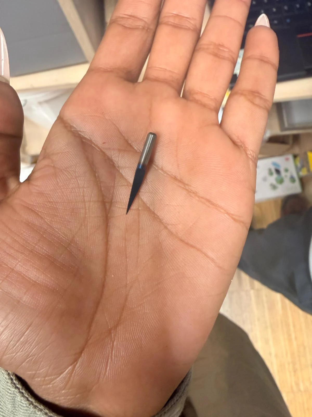
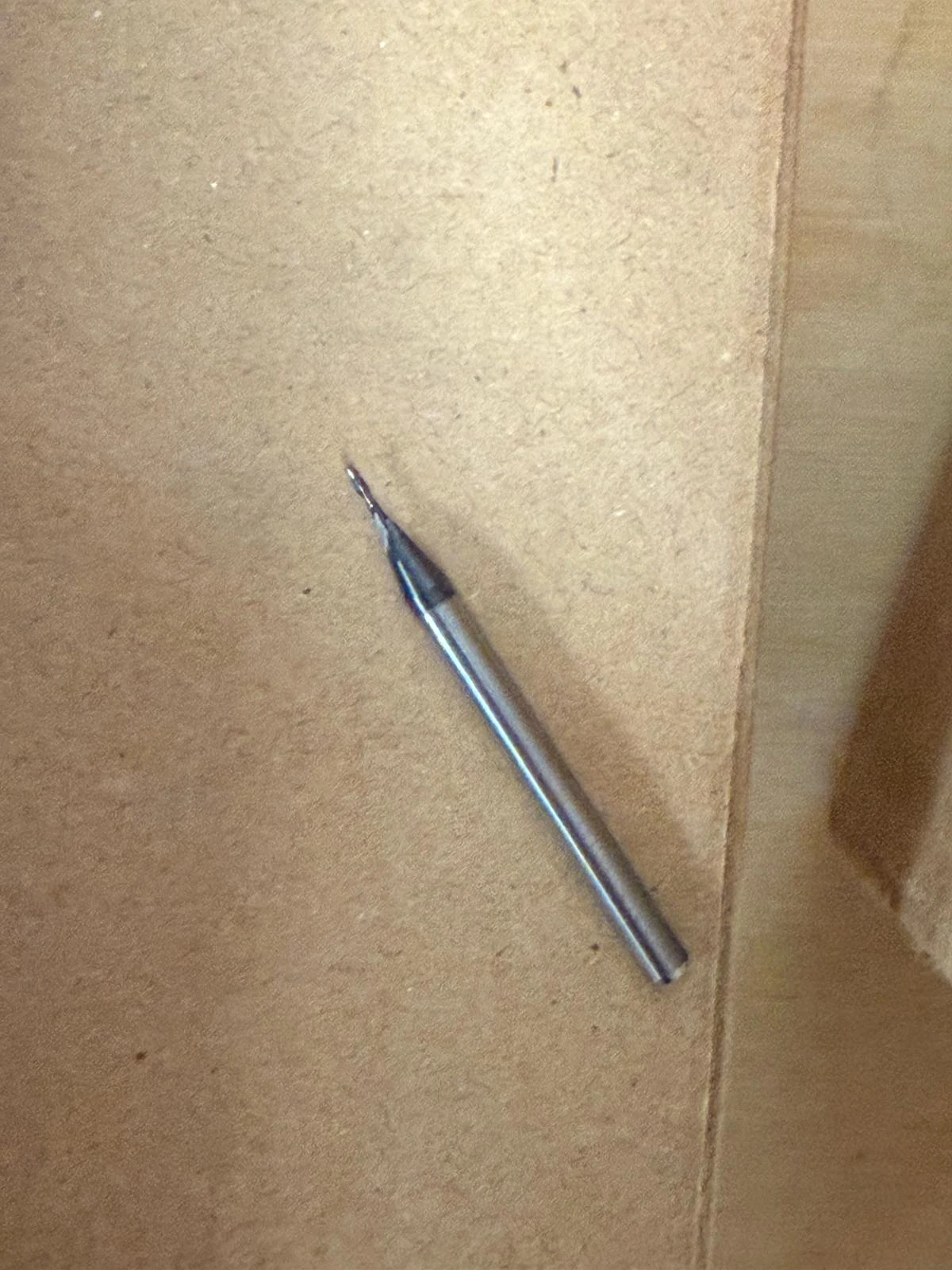
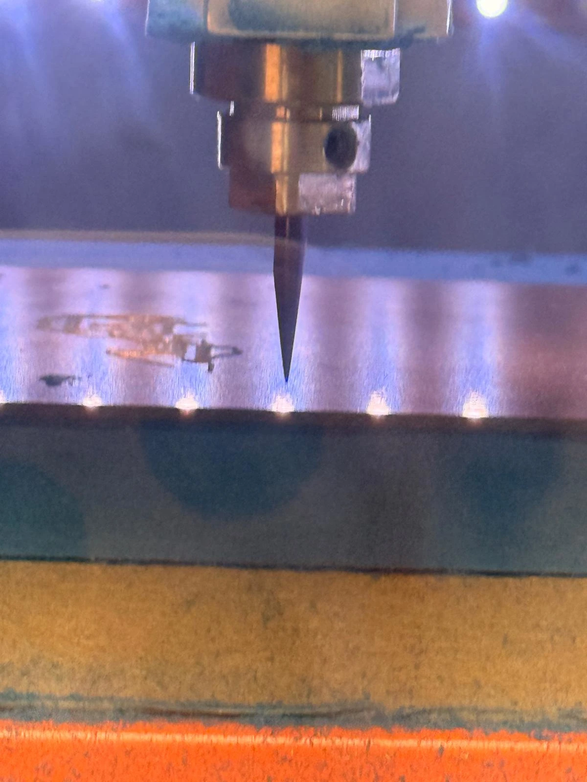
I used a 15° V-bit for the traces & a 1/32 flat bit for cutting the outline.
From mods.ce export the 2 .rml files & transfer to a usb drive & import into laptop connected to the Roland SRM-20 that is used for cutting.
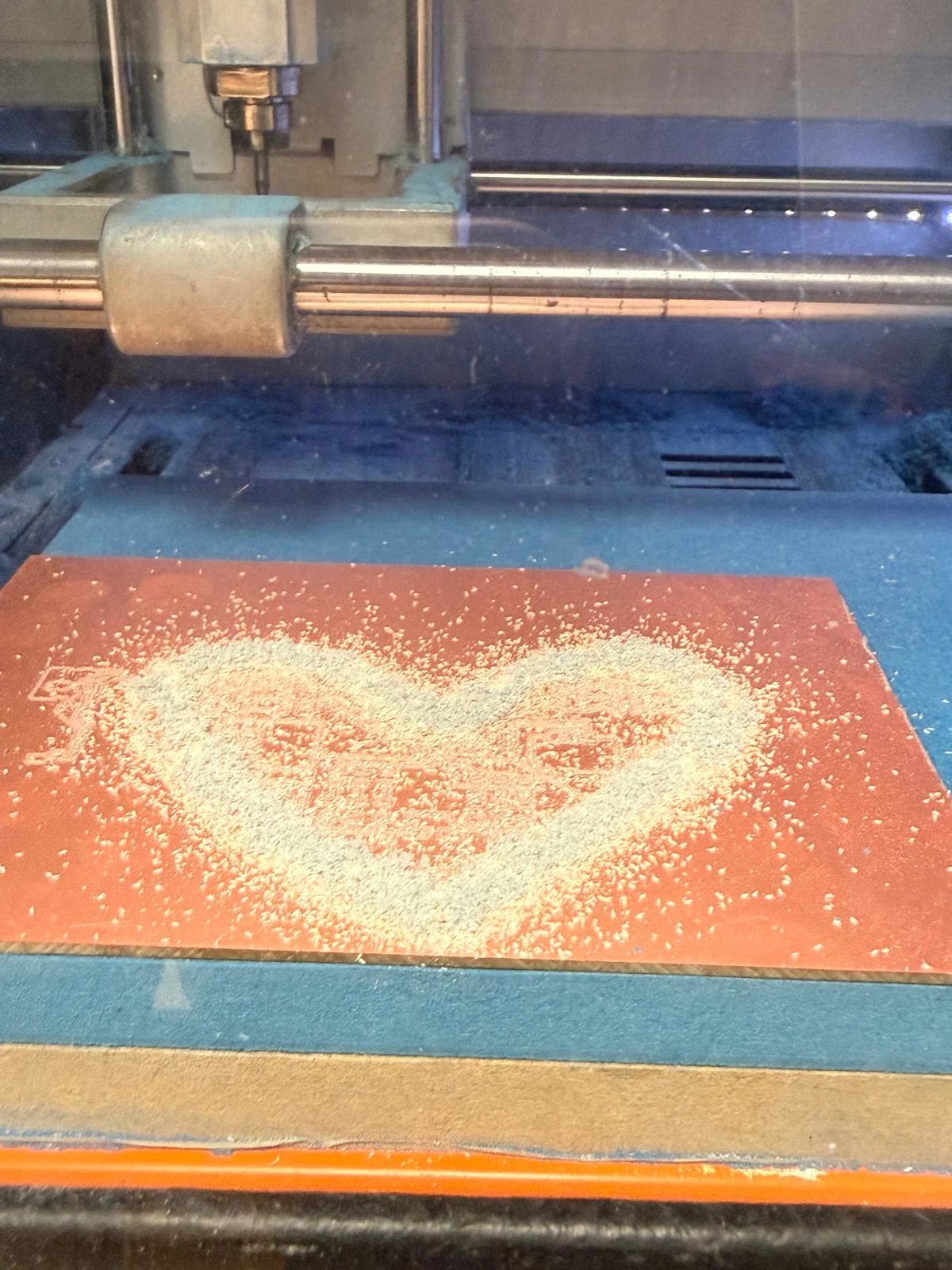
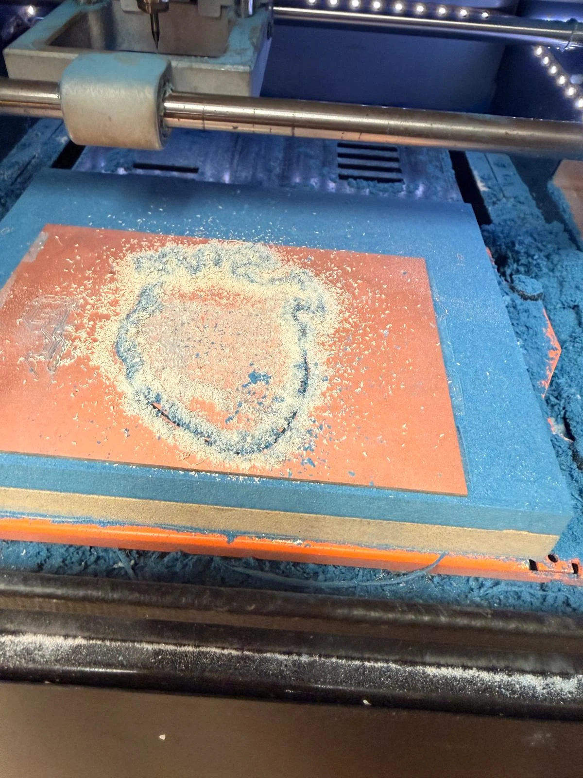
I used a bigger single sided copper + composite sheet that was 100 x 130 mm. Cut the traces first, then the outline so that the piece doesn’t move while milling. During the first try, the mill bit only reached the surface on one side & it was moving in the air and not touching the board, so we made a flat cut on the sacrificial layer and put the material on it again.
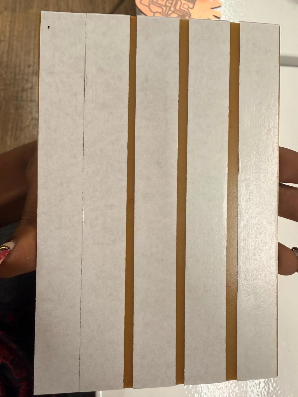
To start the physical production, have the RML files ready in the laptop of the machine. Prepare the copper sheet by applying even strips of thin double sided tape without any folds. It helps to fold the strips of tape extended over the sides & pull the tape flat to ensure there are no folds even later when removing the double sided layer of plastic. Clean with acetone to remove the residual glue first.
Lay the material flat on the sacrificial bed. Install the V-bit into the holder, use the allen key to open the holder and use it again to tighten. Ensure that the bit is held securely and can move down slightly to set the Z-origin. Press the material flat down to make sure it is fully flat. Move the base with x & y movers on the V panel software to set the XY origin at the corner. Do not change this until the end. Then set z by moving down 1mm at a time & when it is close to the copper, lower the bit & let it fall to the surface (only very little, not a big fall). When the bit is touching the surface, tighten the toolbit & set the z-origin.
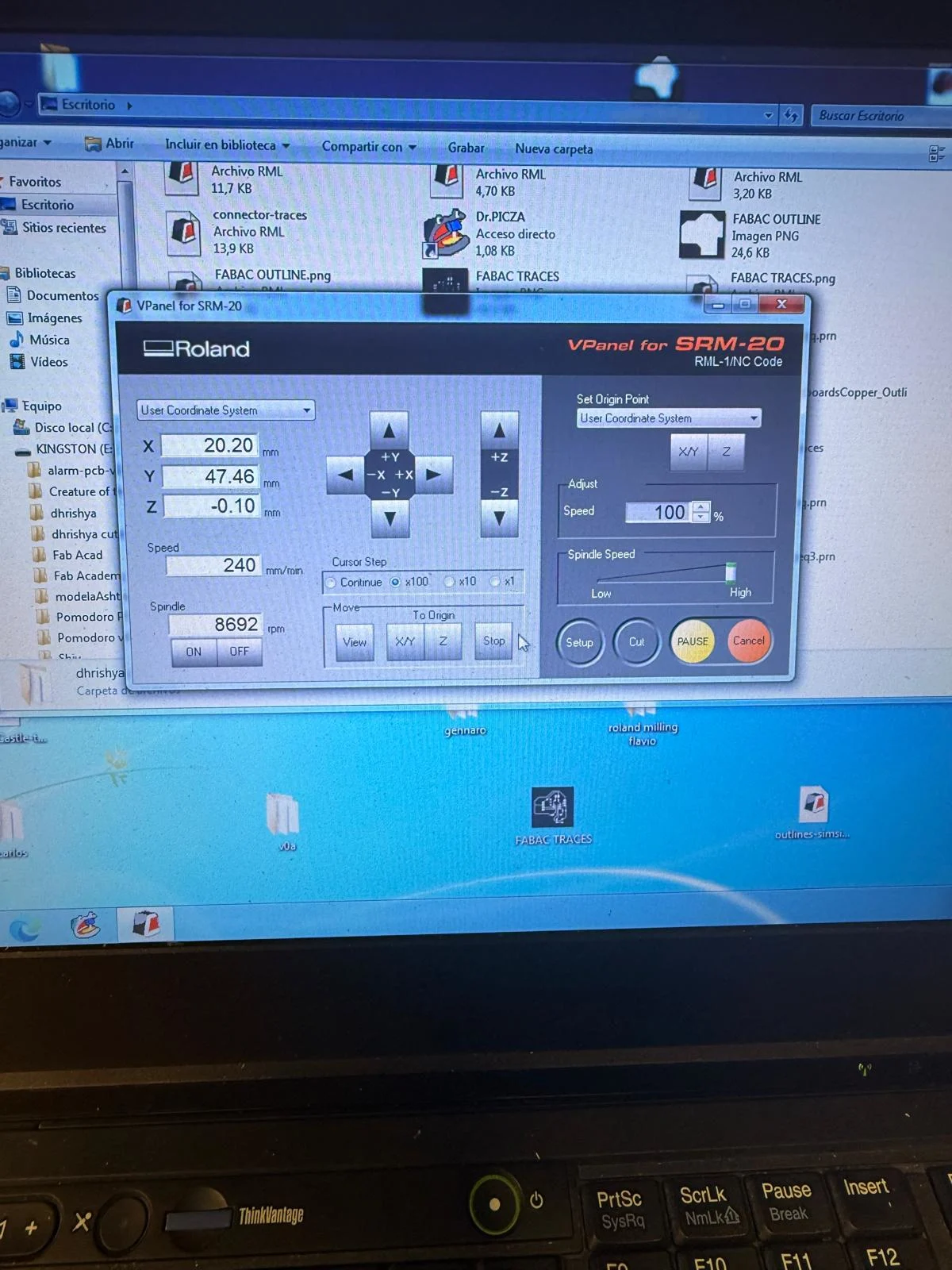
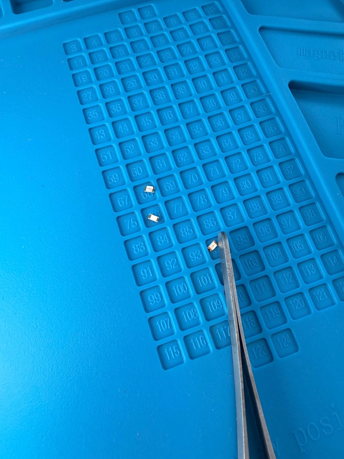
Make sure to keep the allen keys & other bits stuck to the magnets inside the enclosure. Add the traces .rml file & start the cut. Once the traces are done, dust off the excess material removed with a brush & change the bit to the 1/32 flat. I made the tool up to change the bit to the 1/32 flat. Change the z-origin setting process (Do NOT change x & y only z).
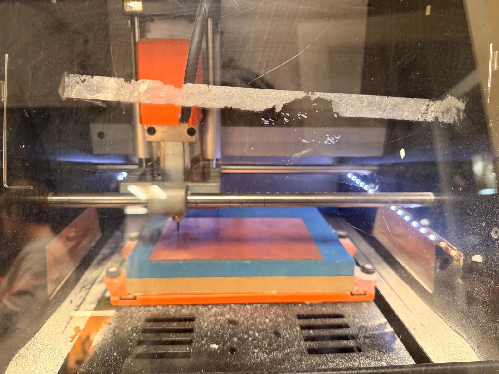
Then I delete the traces file & add the outline .rml & start the cut again.
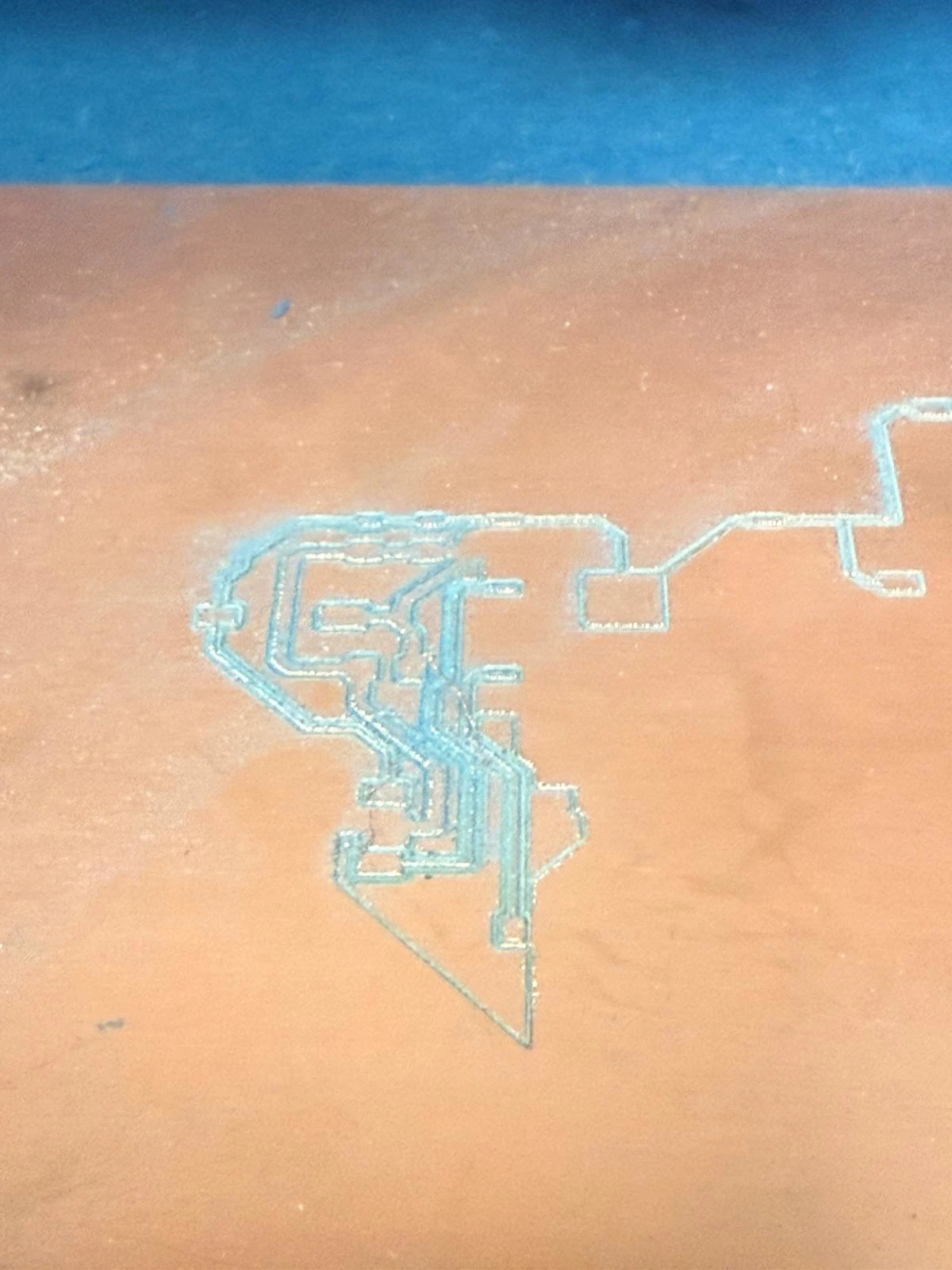
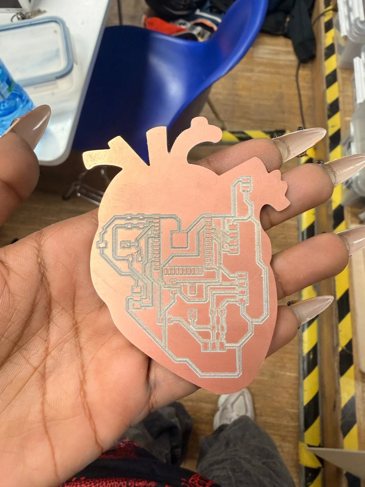
Here is the final boards after tracing & cutting out.
I clean it with alcohol, scrub the excess material from the surface as softly as I can & start collecting the components I need for soldering.
Here is the list :
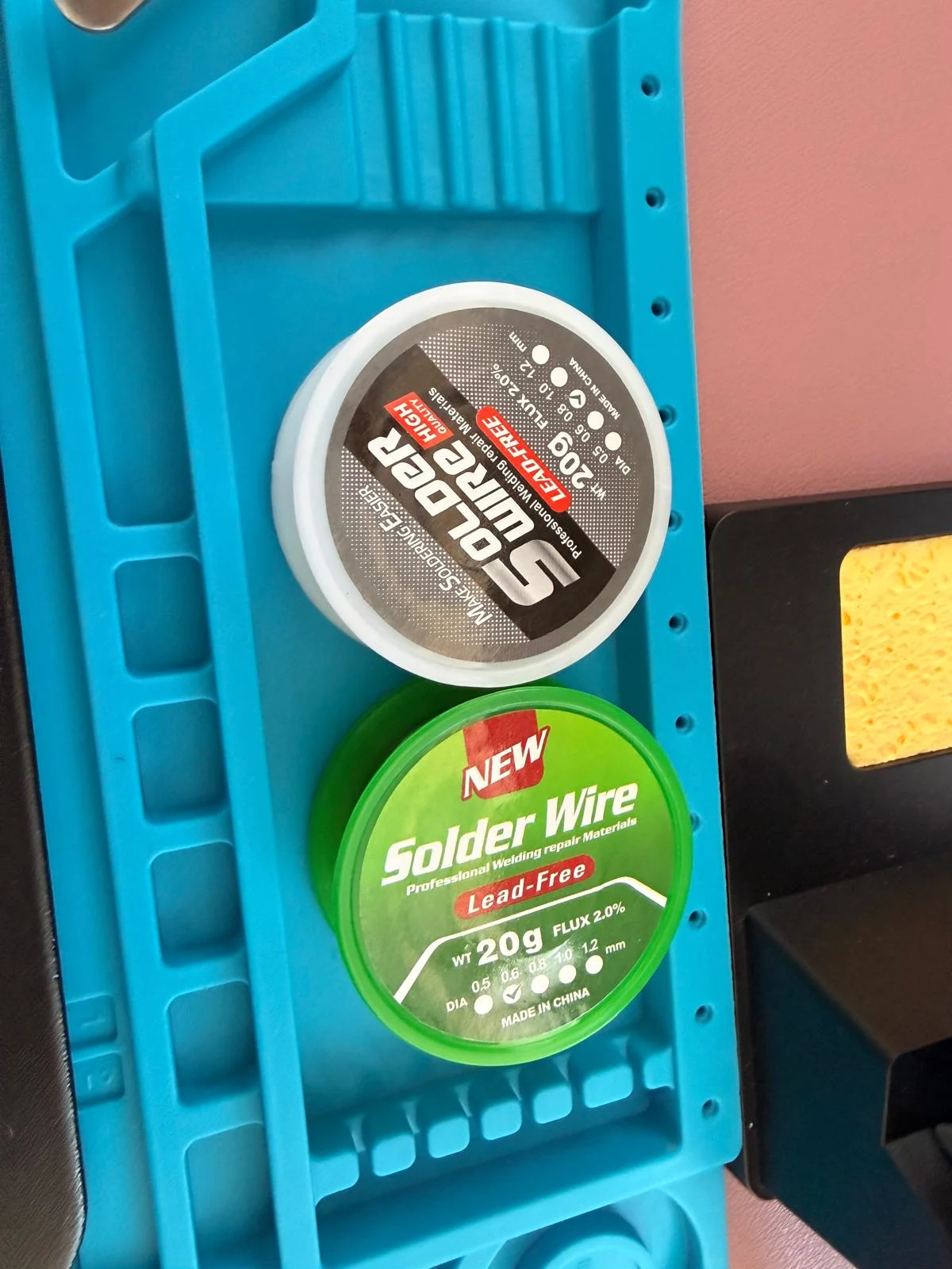
List of materials
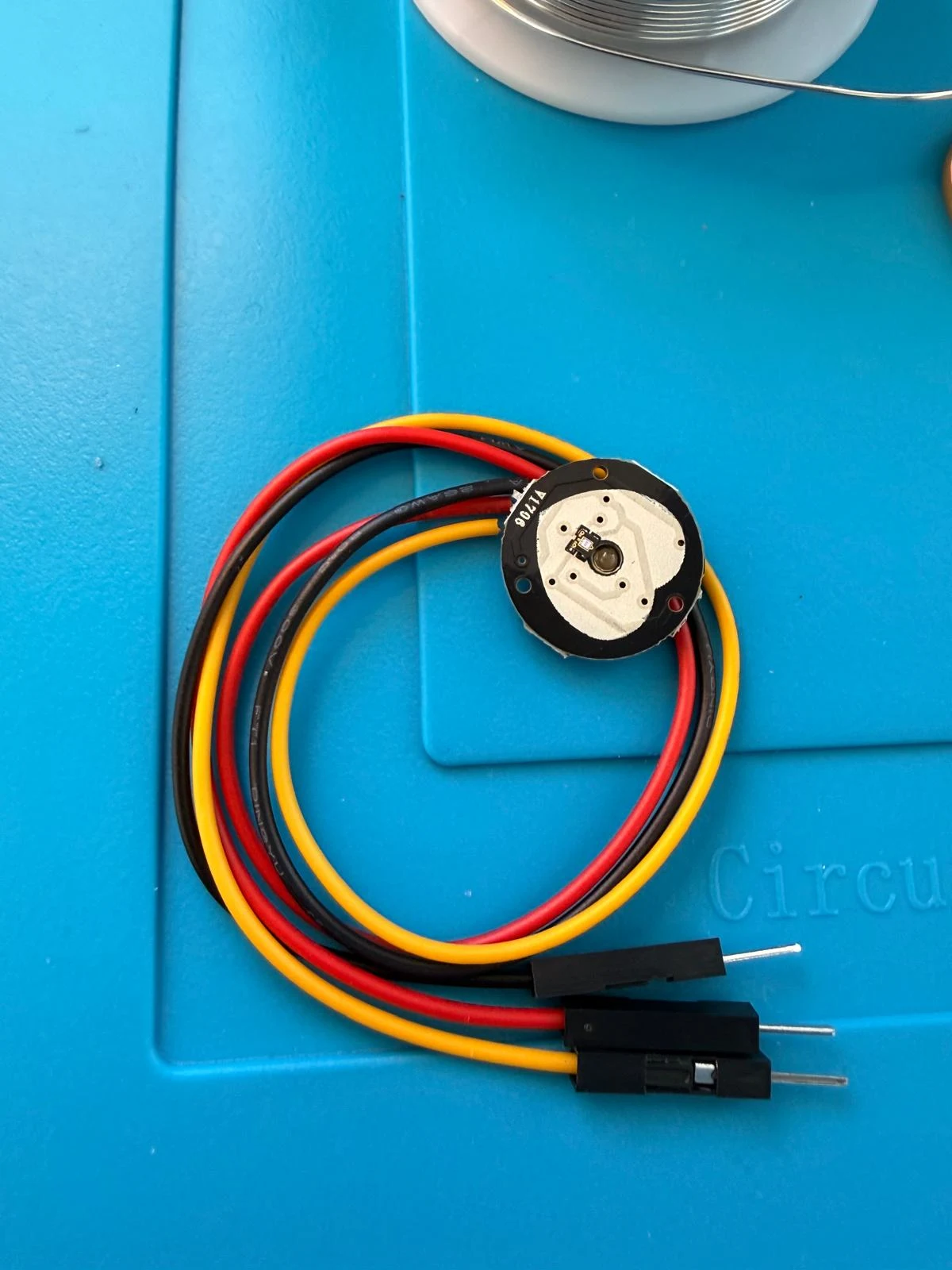
1. Board 1 ♡
Component
I tried to connect Board one with the following steps:
LED RED ×6
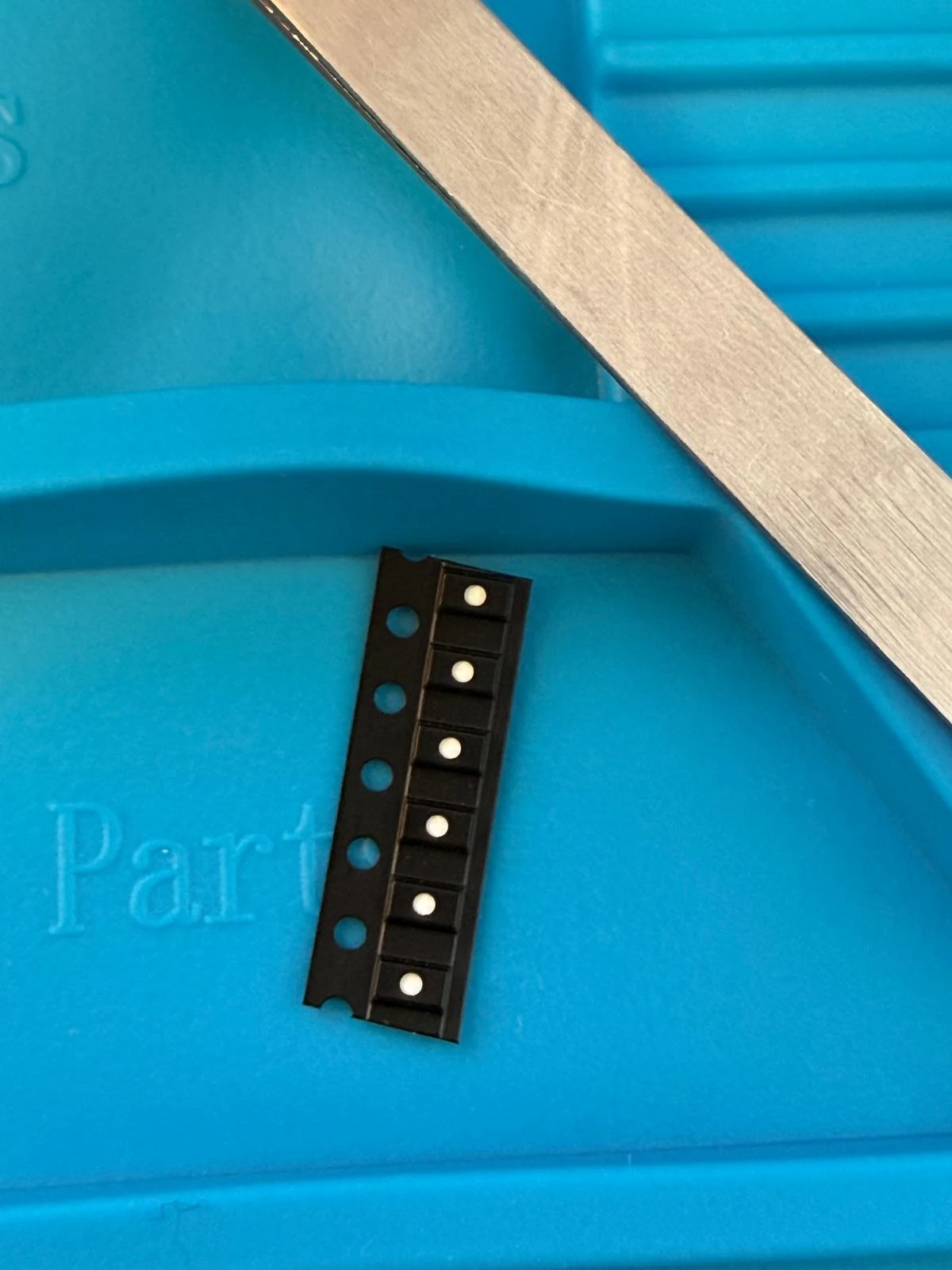
LED BLUE ×6
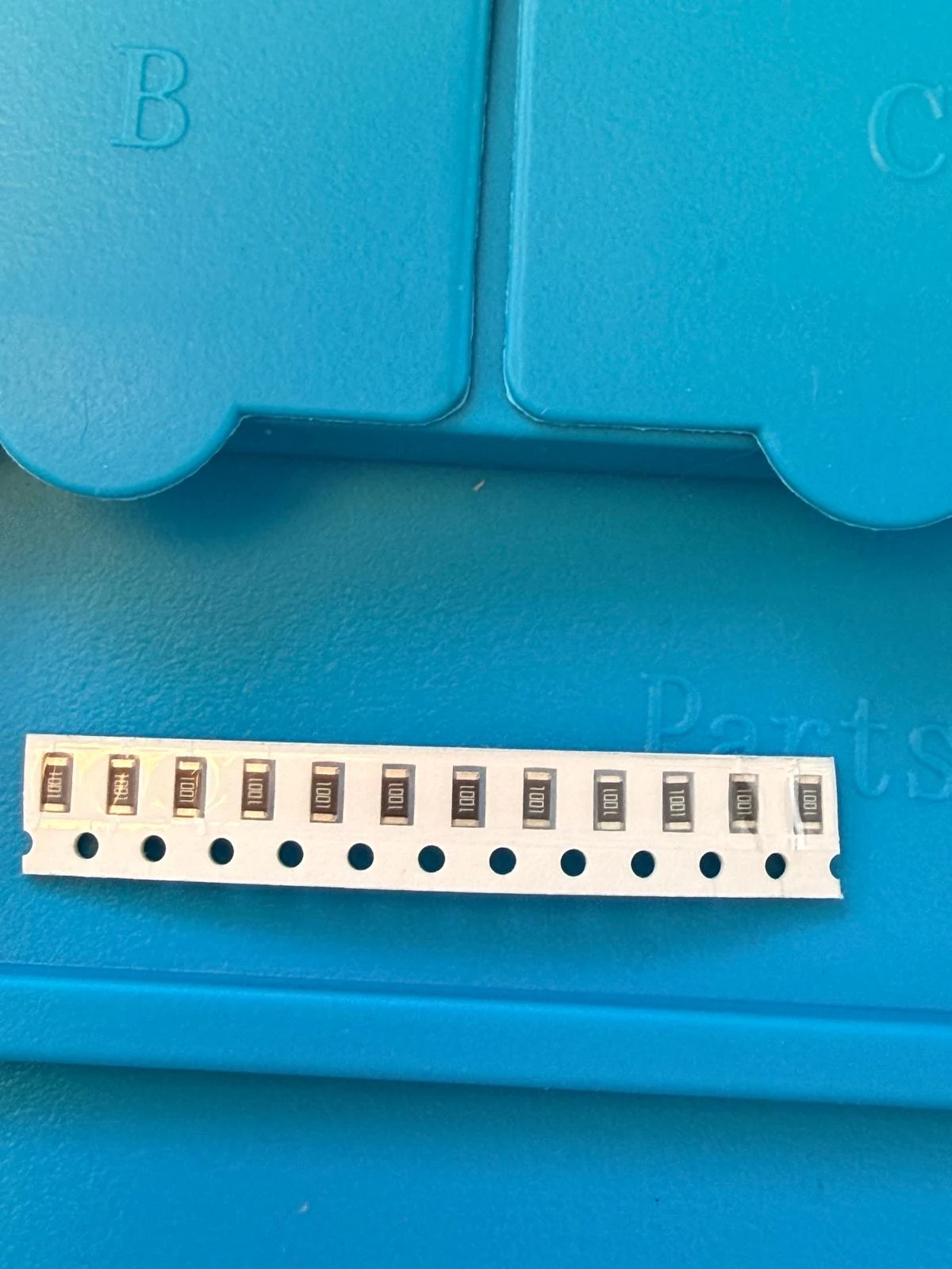
Resistor 1K ×12
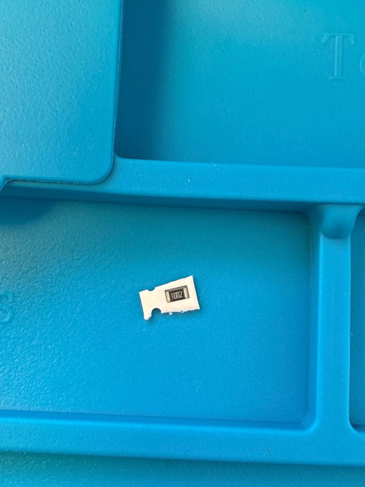
10K ×1
capacitor 0.1uF
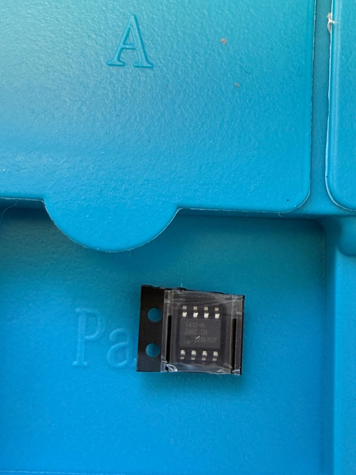
ATtiny 412
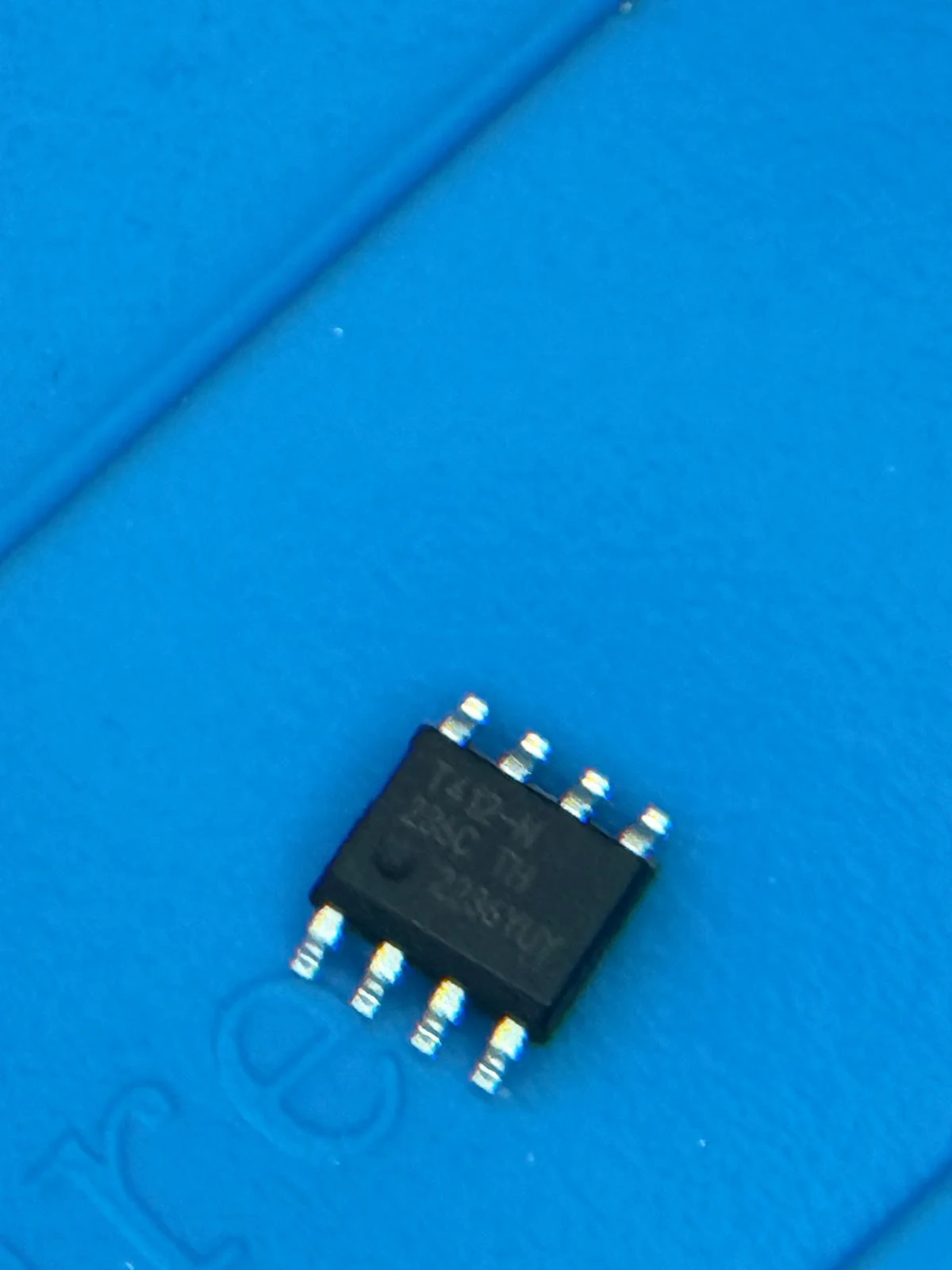
* updi
2. Board 2 ♡
Resistors ×3
10k ×2
330 ×1
Capacitors
0.1uF ×2
10uF ×1
1000uF ×1
Button ×2
2 pin
esp32 wroom
+ neopixel
+ oled
+ pulse sensor
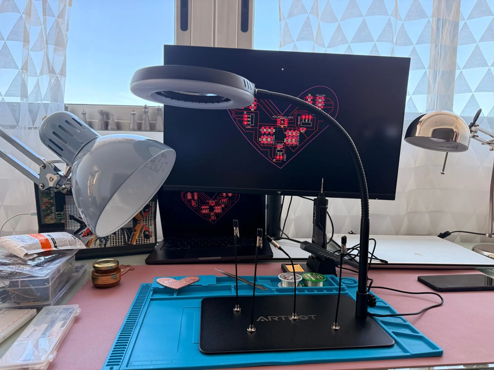
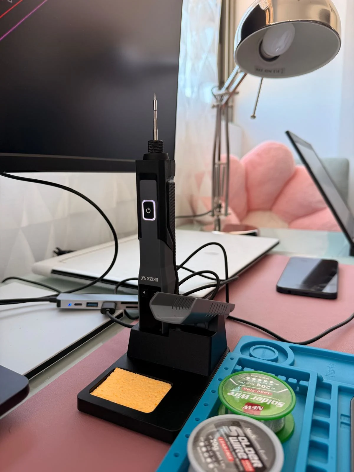
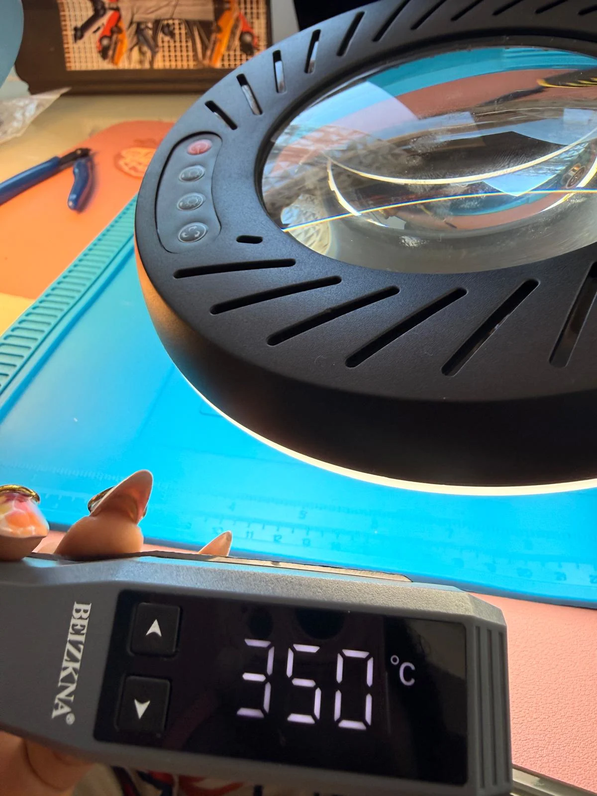
I then set up my soldering station & use the following components & a handheld battery powered soldering gun at 370° to attach the components.
Soldering notes:
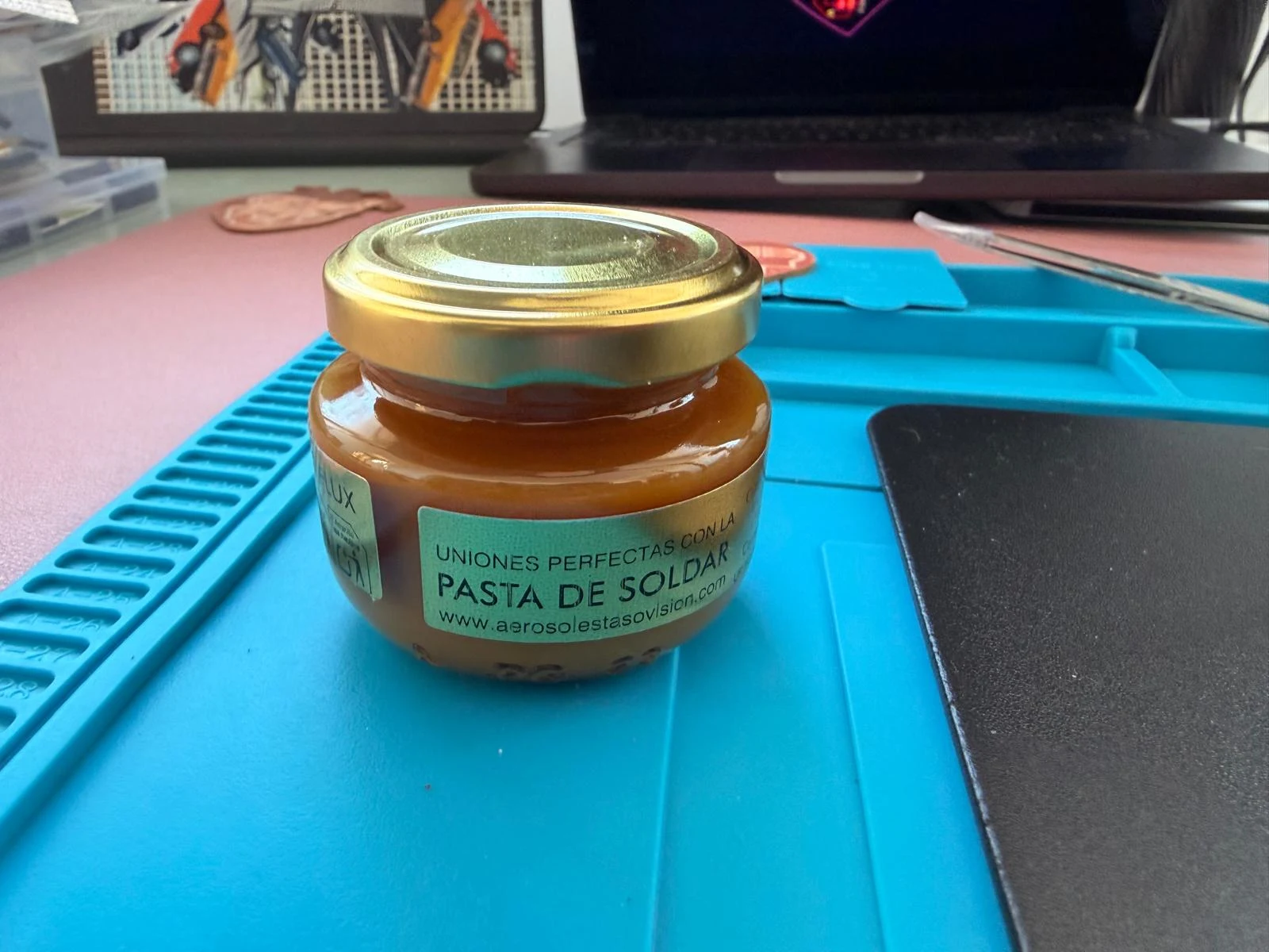
* coat the components in flux & a bit of solder metal.
* have the connection diagram open on a screen & go over it and take special note of polarised components.
* peel the plastic tape & remove the component from the casing.
* heat the pad and then add some solder material to the pad.
* use tweezers to hold the component in place & add heat to let the flux flow through the pad & component and melt the solder.
* then add some solder to the other side (pre coated) to fix it to the board.
* add extra solder to create a bed & secure the component.
* the resistors & capacitors are non-polarised but the ATTiny & ESP32 had a specific direction indicated by a dot in the corner of the component and the PCB diagram of traces.
* Be careful not to hold the solder gun on the pad for too long as it can lift the traces.
Arduino
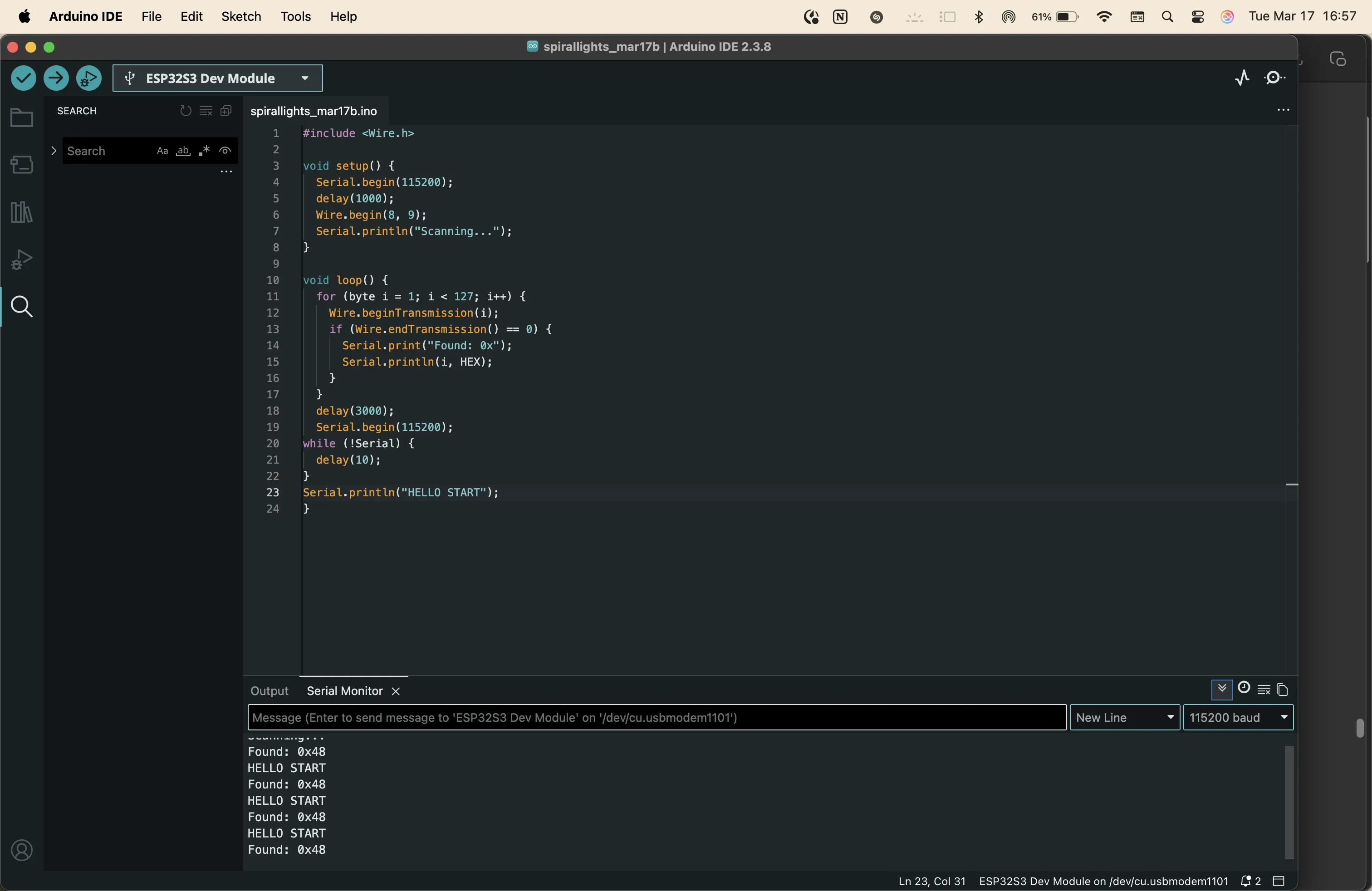
Challenges
* Only 2 of the LEDs lit up on board 1.
* The ATtiny board was not reading on the computer.
* the remains from milling made the board uneven & difficult to hold the components when soldering.
* the fragments caused the 3V3 & GND to cross & made a tiny explosion in the ATtiny & caused a small electrical smell. I want to redo this board by rearranging the traces further apart & using a 1/64 bit for tracing so I can have cleaner results.
* when connecting the esp32 to the other boards, I lifted the traces and made the board unusable.
I need to make a breakout board for the esp32 and be better at soldering. I saw some reference videos & practiced again with the non-working board so I don’t repeat the mistakes I made this time in the next version.
updates on boards coming soon after retrial.
Personal Reflection.
I explored differently shaped PCBs & had a great time organising the layout on KiCad to not cross any traces during the first try. The bit only worked on one side of the board so I created a flat layer on the sacrificial layer and tried again. It worked great the second time & I achieved 2 types of boards. The boards don’t work yet because my soldering skills needed a lot of practice & I messed up when connecting the MCU :( I will cut again & update the documentation.
video
original files
group assignment
here is the link to the group assignment page Group Assignment week 8
Reflection
This week I reflect on how precise PCB milling can be. We used the Roland SRM-20 to cut using single sided copper boards. Milling is a multistep preparation process.
→ design circuit
→ choose components
→ schematic design
→ PCB design
→ inverted traces export
→ clean & align DPI on inkscape
→ getting the .rml file for vPanel software
→ add tool
→ set origin
→ cut 1 by 1
My contribution to this assignment focused on helping with the machine preparation process & helped to select the mill-bits, setting the origin & changing the tool as appropriate. It’s important to keep the mill bits safe as they are expensive. Keep the Allen key for changing bits and the other bits needed for the process in the machine on the magnet on the side. It is important that the bed is flat & there are no folds on the tape holding the material to the bed. The surface should be as flat as possible. Move the z axis only 1mm at a time so that the bit doesn’t smash into the bed.
Z-calibration is very important especially when using V-mill bits. The bed is called the sacrificial layer since we can run the flat mill throughout the surface to make it fully flat after every few uses. The V-bits offer more resolution but leaves a lot of residue that needs to be cleaned off later carefully without lifting the traces.
This process needs a lot of trial & error but once finished gives a complete finished clean output that can be used for system integration.
notes
Put your notes here.