Individual assignment:
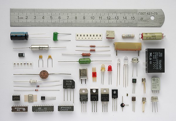
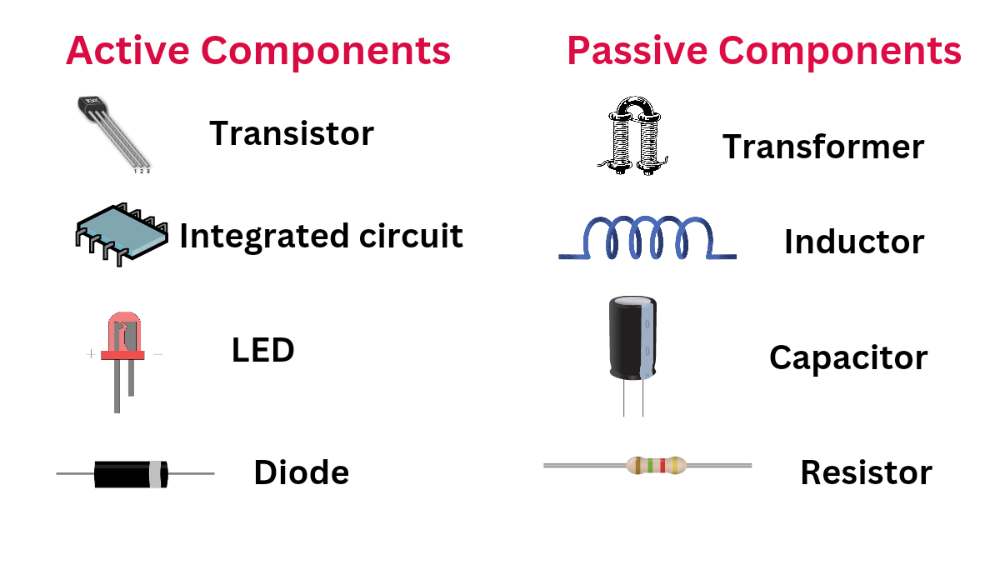
Electronic design is the process of selecting and combining various electronic components—such as resistors, capacitors, ICs, and transistors—to create a working circuit or device.
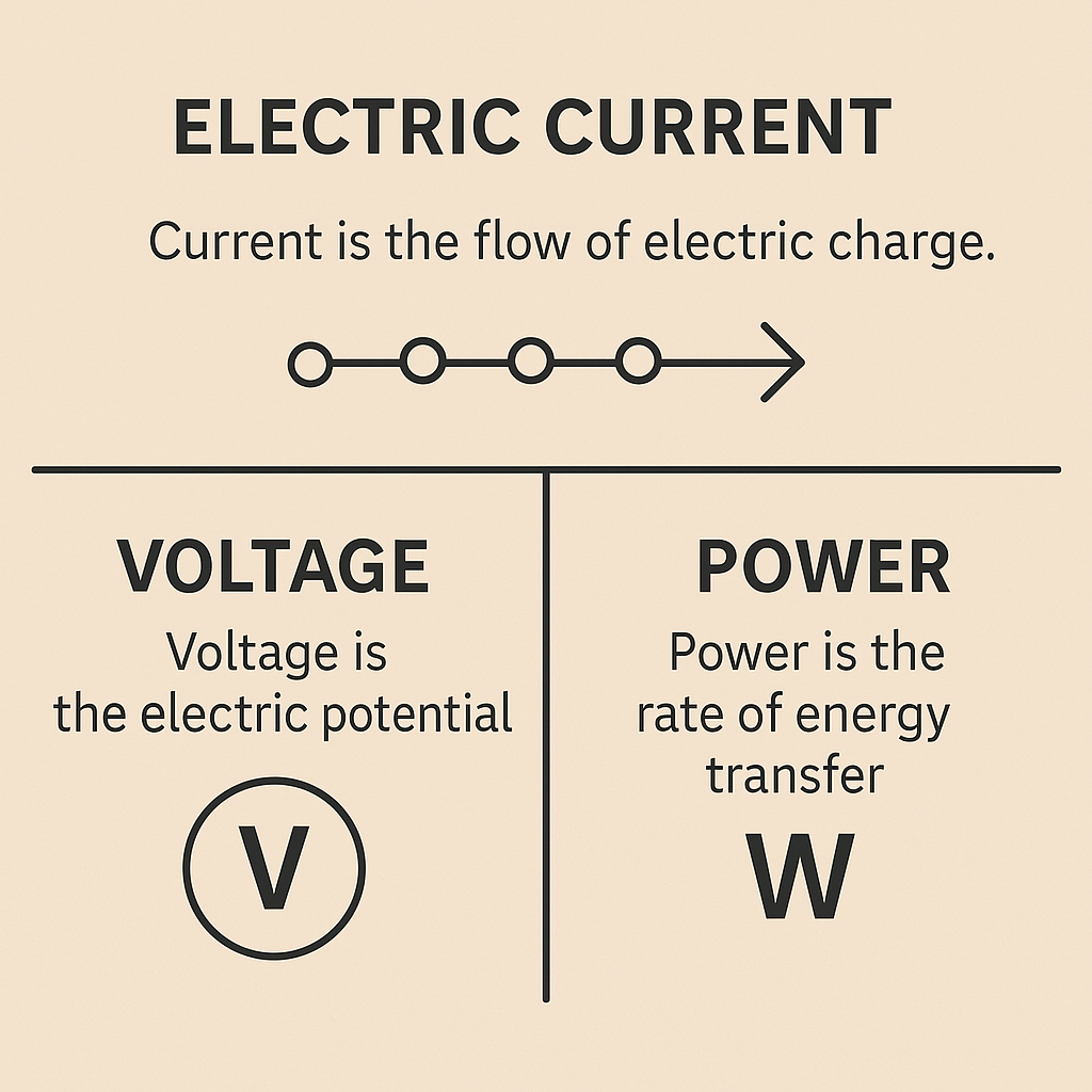
Voltage - the electric potential between one place and another. How much the electricity wants to move from one point to another. Measured in volts.
Current - the current flow from one point to another, literally based on how many electrons are moving per second. Measured in amps
Power - work that is being done per second. In circuits, this usually means the amount of heat given off by a circuit. Measured in watts, or joules per second.
Energy - total amount of work done. There is no time component for this, which is the differentiator between power and energy. Measured in joules. These are clarified more later in this tutorial.
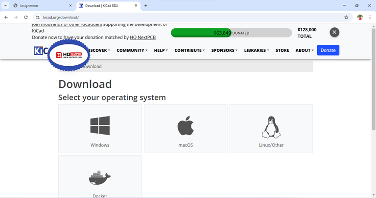
 More info click the link
KiCad is an open source software suite for Electronic Design Automation (EDA). The programs handle Schematic Capture, and PCB Layout with Gerber and IPC-2581 output. The suite runs on Windows, Linux and macOS and is licensed under GNU GPL v3.

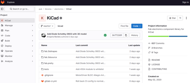
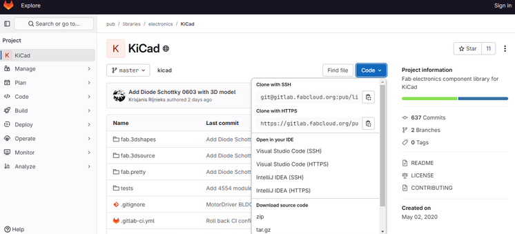
In our Fab Academy course, we were introduced to the Fab Library, a crucial resource that contains all the components required to design a printed circuit board (PCB). By installing this library, we ensure that all the necessary components are available in the design software, making the design process more efficient. The library is specific to the components you need for your project, which is why I downloaded the Fab Library for my assignment.

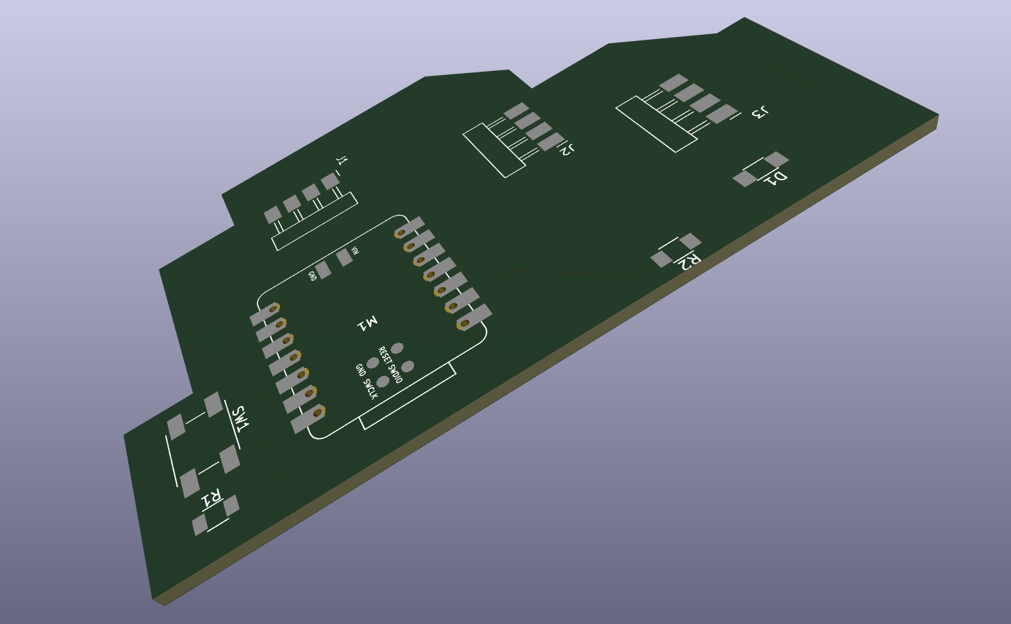
I began my journey in PCB design by utilizing the RP2040 microcontroller. In this project, I incorporated a variety of components, including three 4-pin connectors, an LED, and a switch.
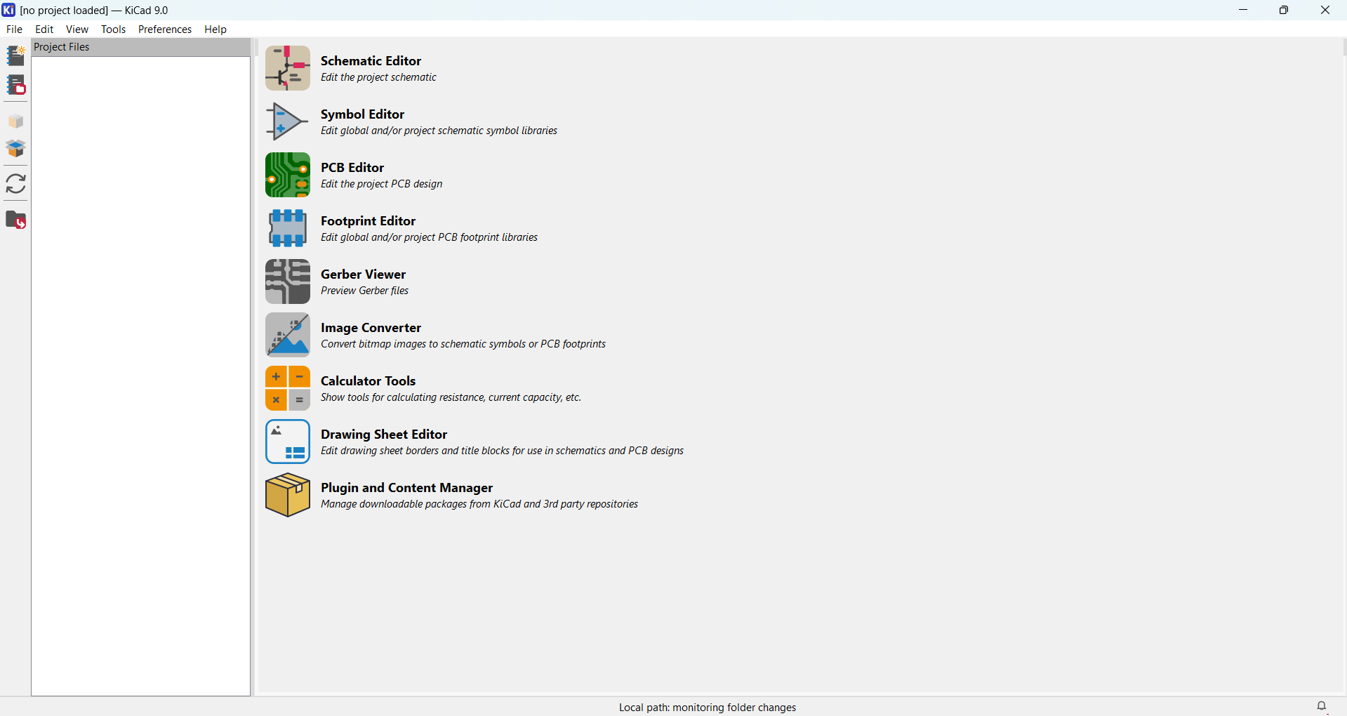
I launched the KiCad software to kickstart the design process.
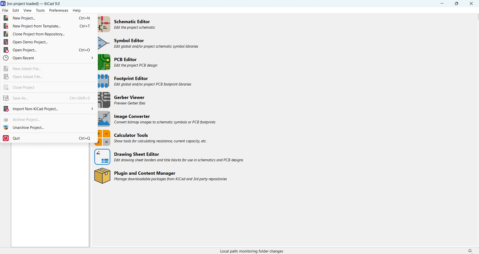
A new project was created to initiate the schematic design phase.
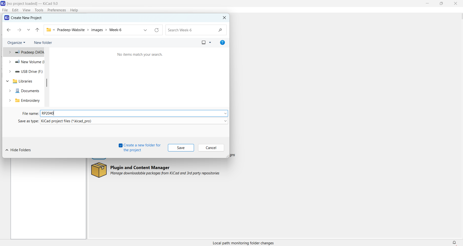
I specified the project file name and saved it to ensure proper documentation.
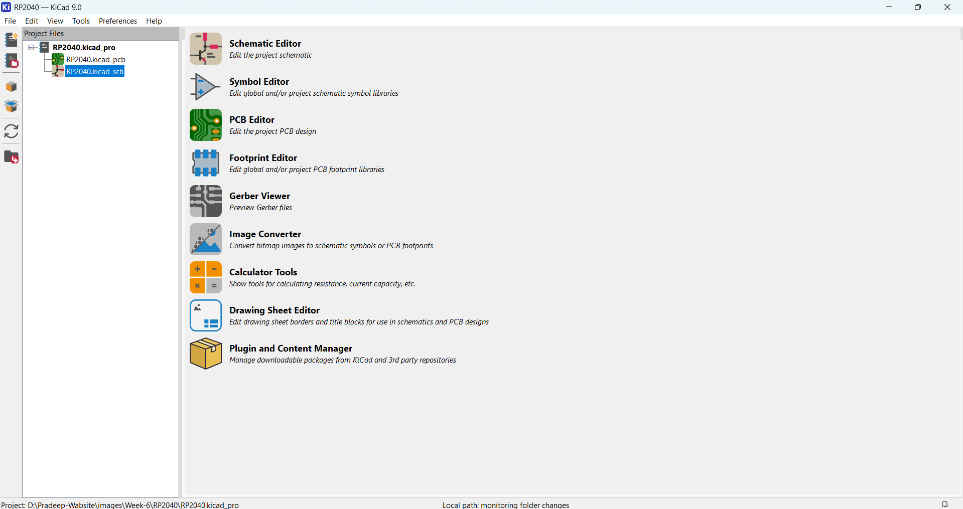
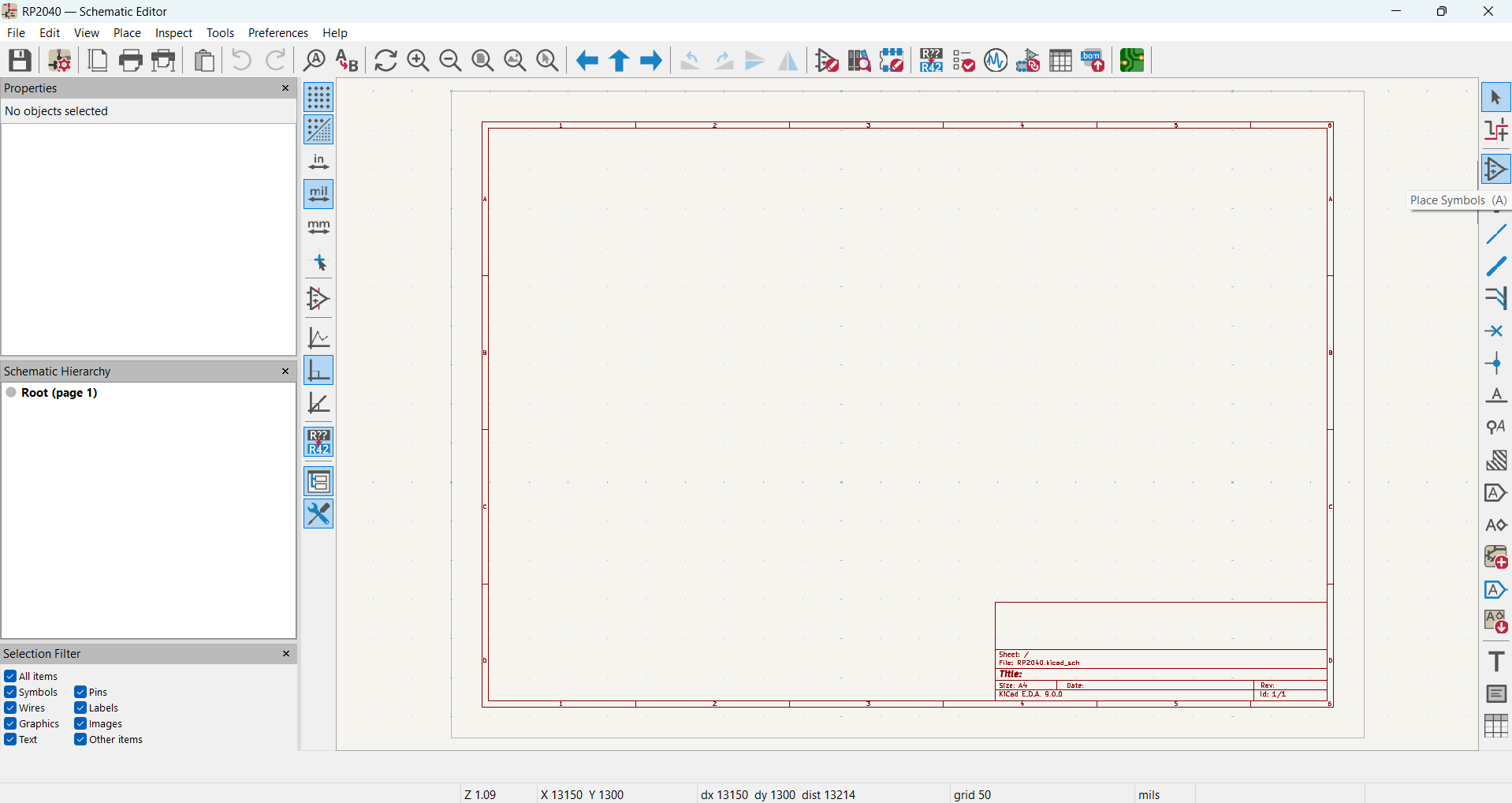
The schematic editor was opened directly from the KiCad main window to begin placing components.
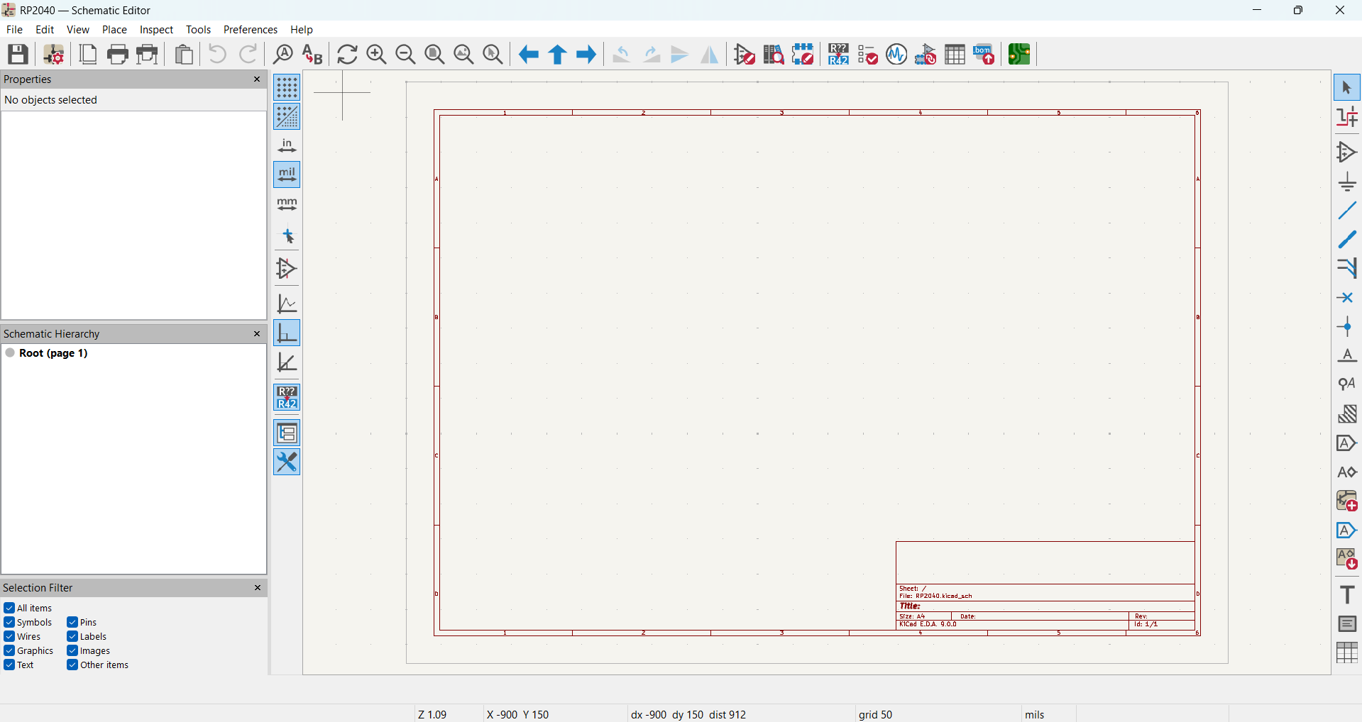
The schematic page was successfully launched, and I started placing the components as needed.
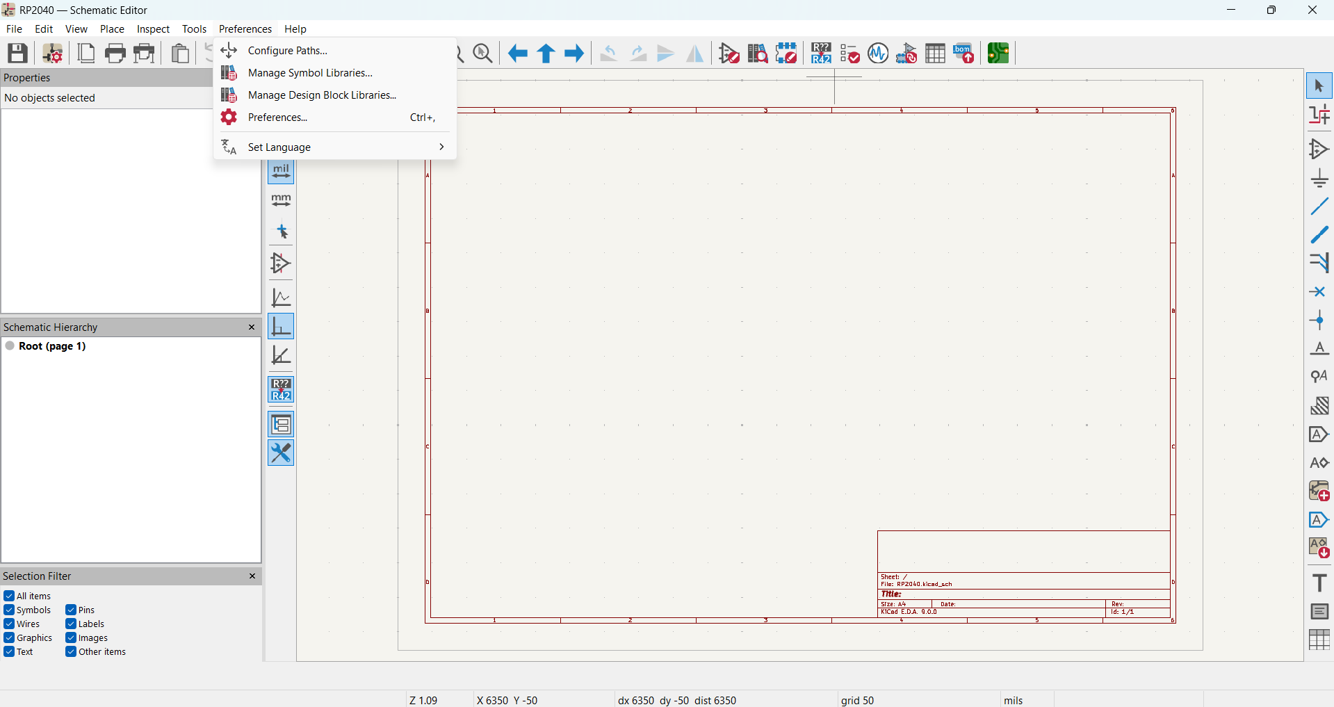
To enhance the schematic, I navigated to the Preferences menu and selected 'Manage Symbol Libraries.'
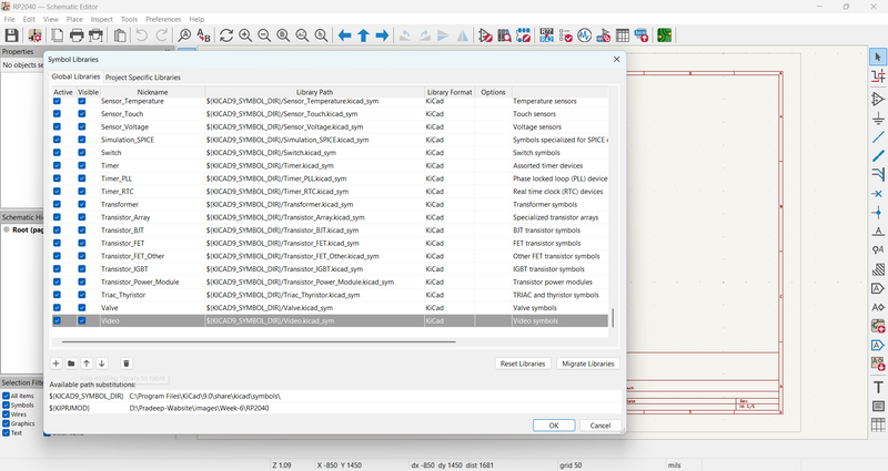
I accessed and browsed the external symbol library file for additional components.
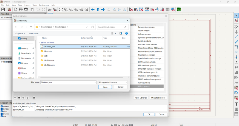
I successfully loaded the `Fab.kicad_sym` file from the Fab Library to incorporate the necessary symbols.
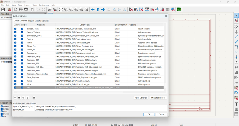
The Fab Library was successfully loaded, and I confirmed the process by clicking 'OK.'
After loading the symbol library, I selected the symbol icon to begin placing the components on the schematic.
Once the symbol library was loaded, all required components became available for placement.
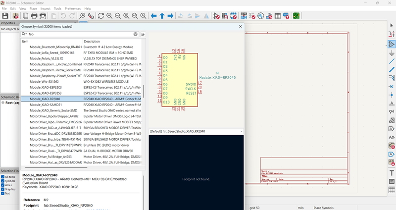
I selected the necessary components, including the RP2040 microcontroller, connectors, LED, and switch.
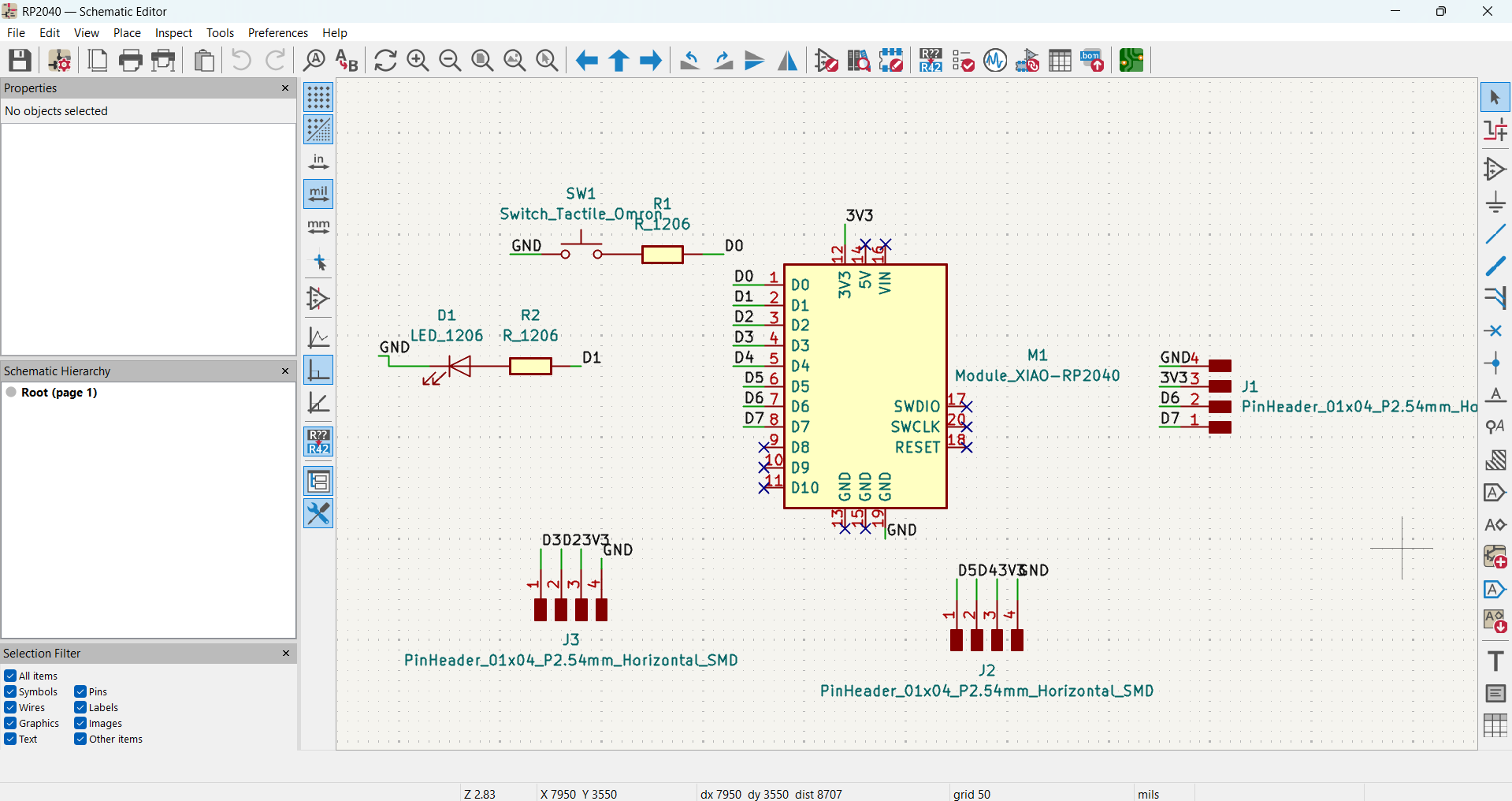
The schematic diagram was completed by placing and connecting all the selected components.
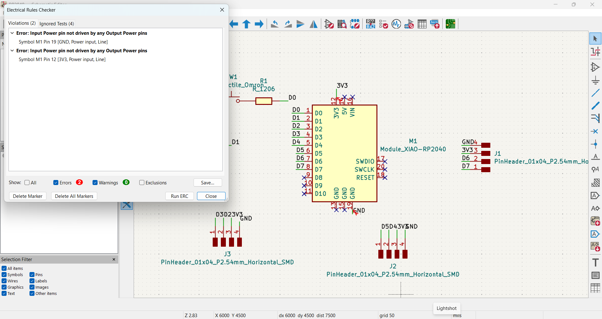
I conducted an Electrical Rule Check (ERC) to identify and resolve any potential schematic errors.
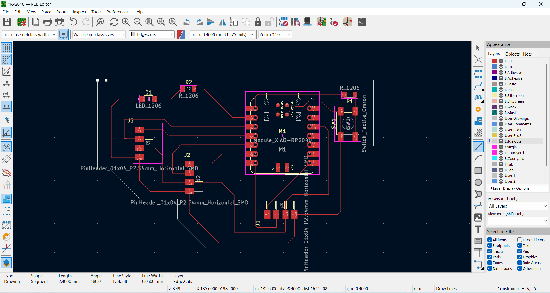
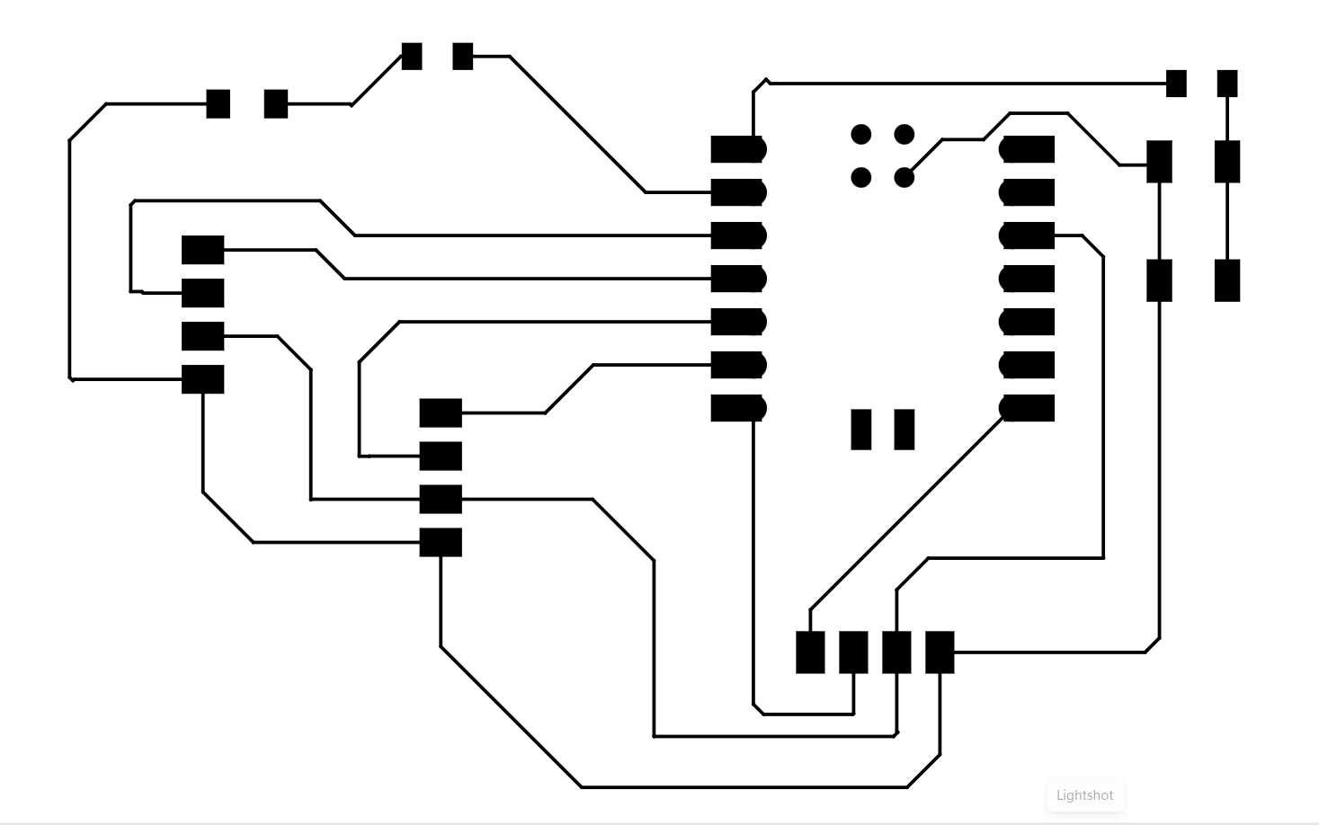
Once the schematic was complete, I opened the PCB Editor to begin the board layout design.
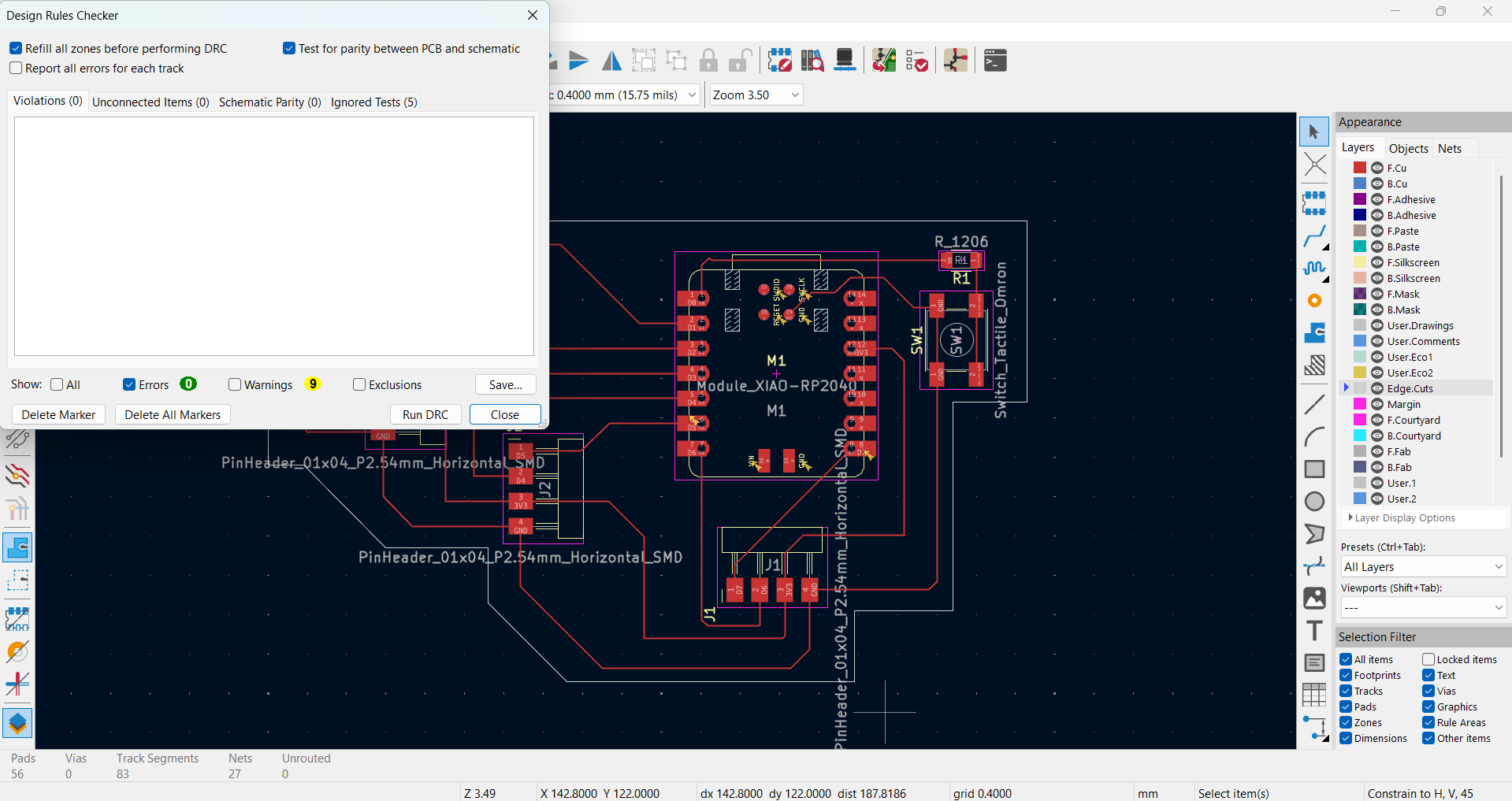
I ran the Design Rule Check (DRC) to ensure that the design met the necessary spacing and layout standards.
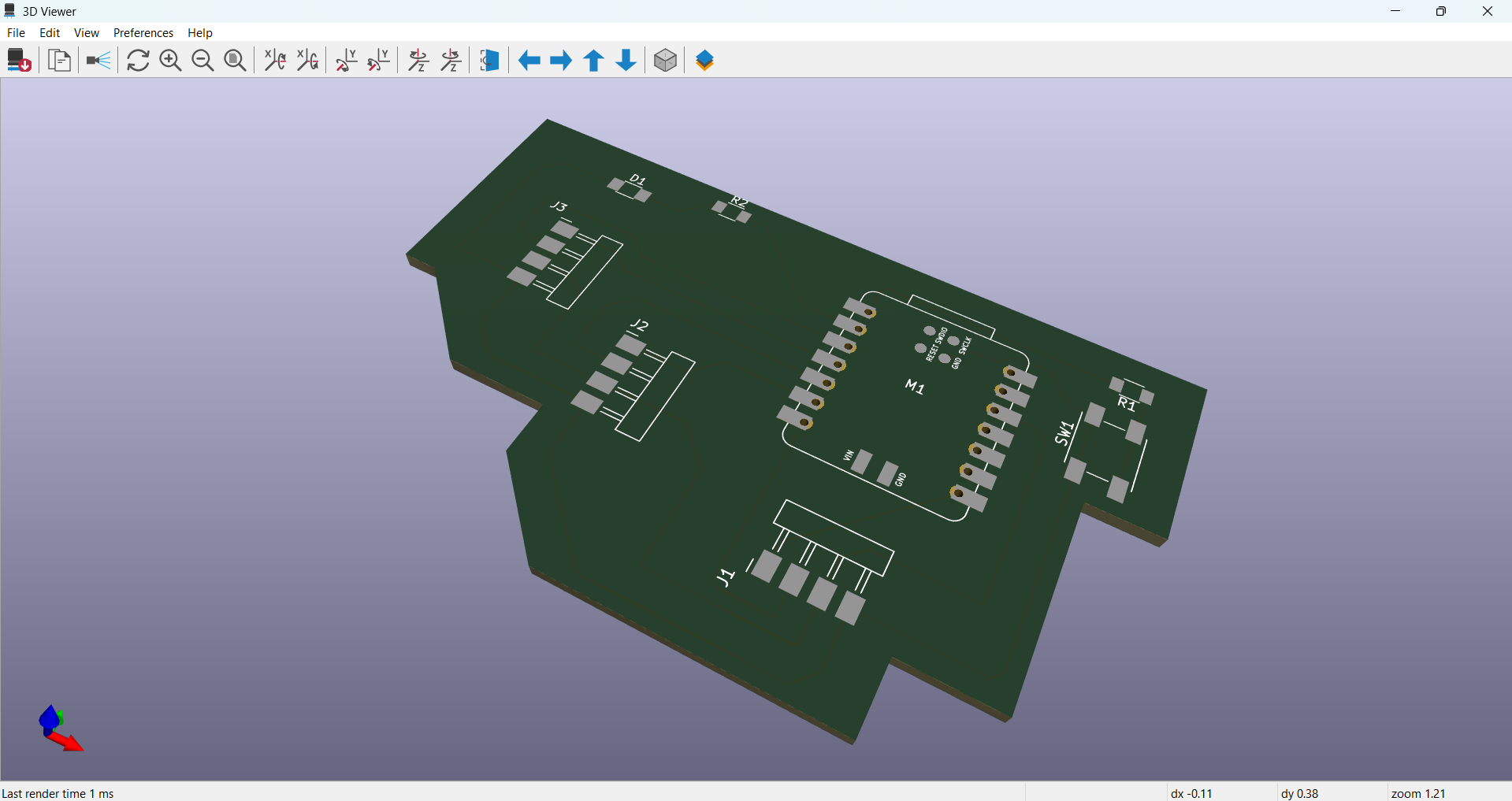
The PCB layout was inspected in 3D mode to verify its accuracy and check for potential issues.
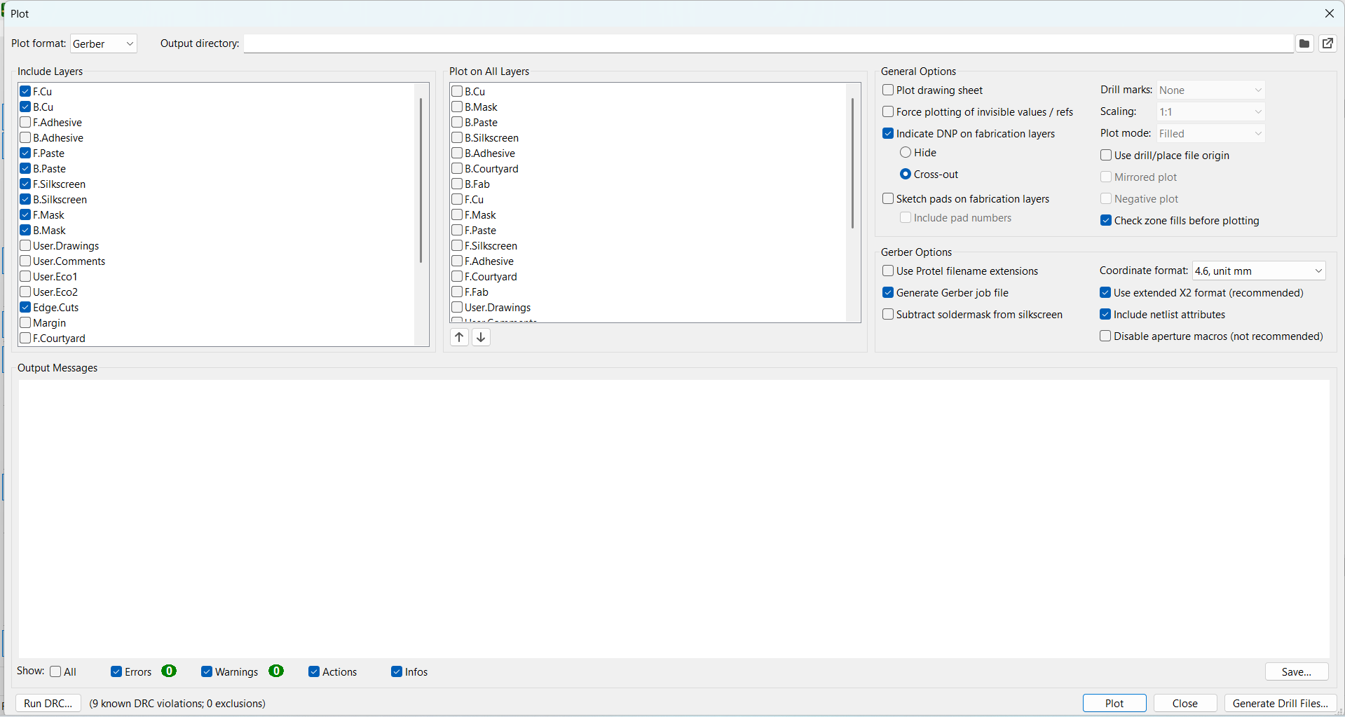
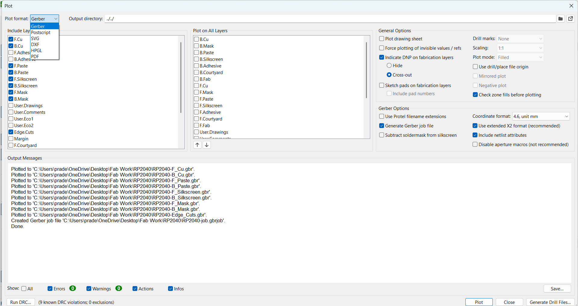
I used the 'Plot' function to generate the output files required for manufacturing the PCB.
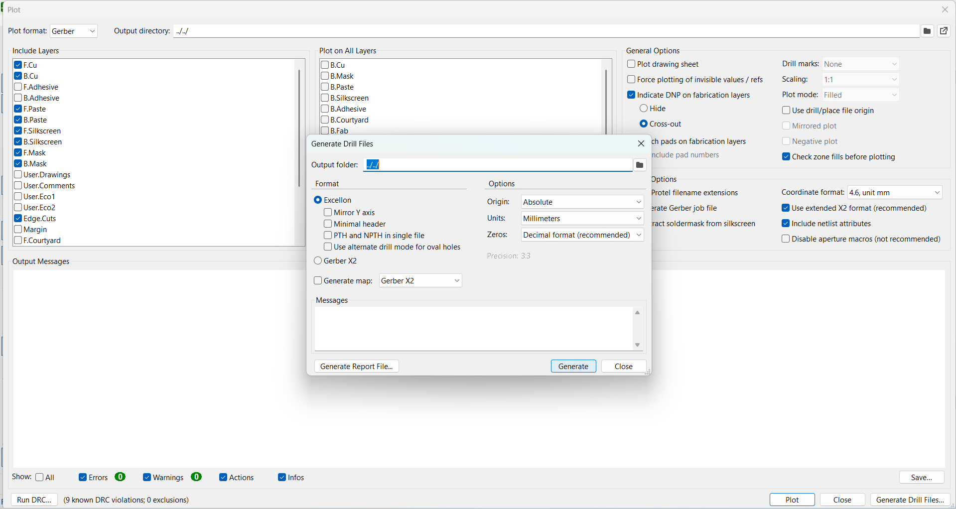
Gerber files necessary for PCB fabrication were generated successfully.
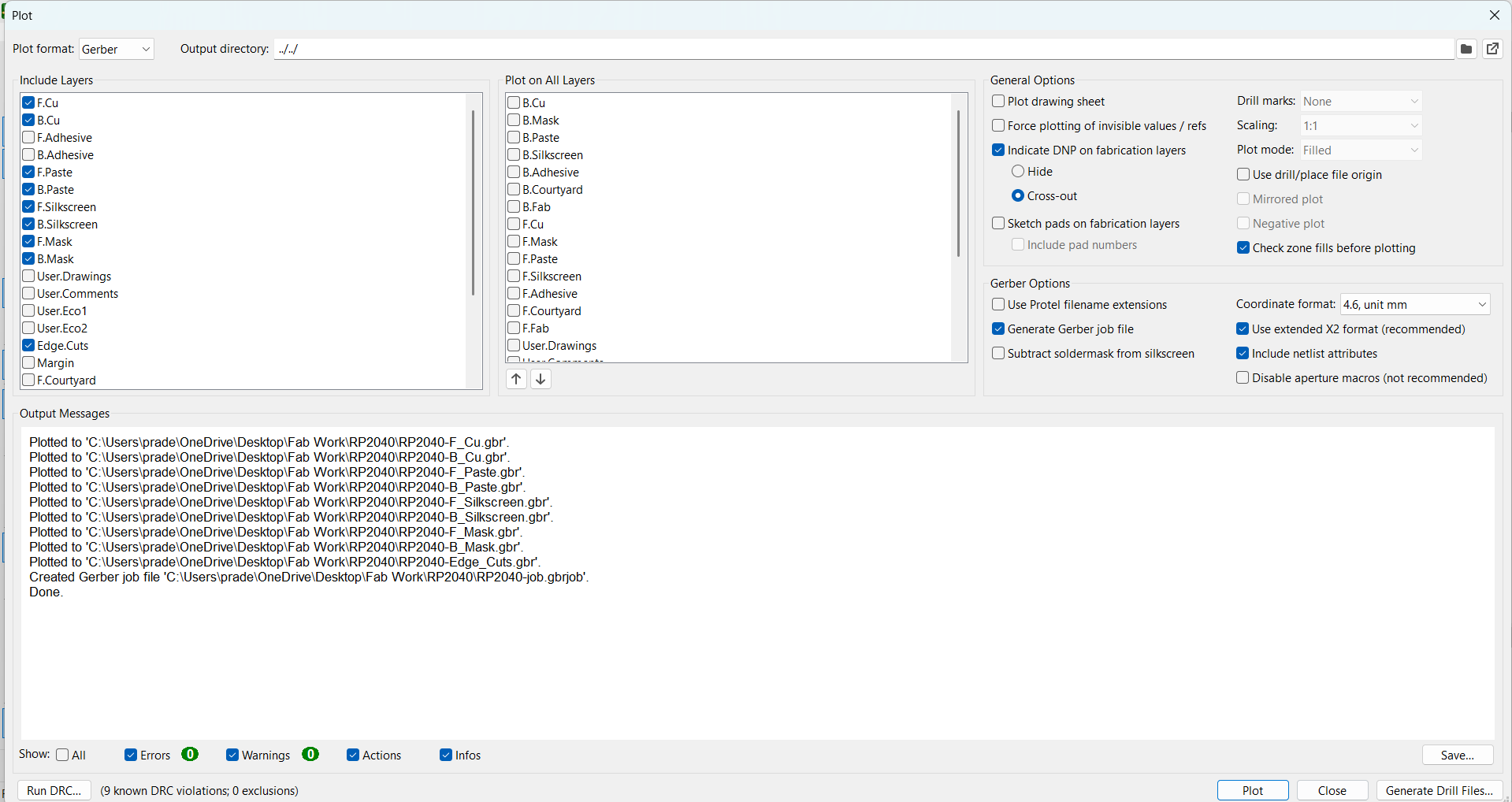
All layers were thoroughly verified in the 'Plot' window before exporting the design files.
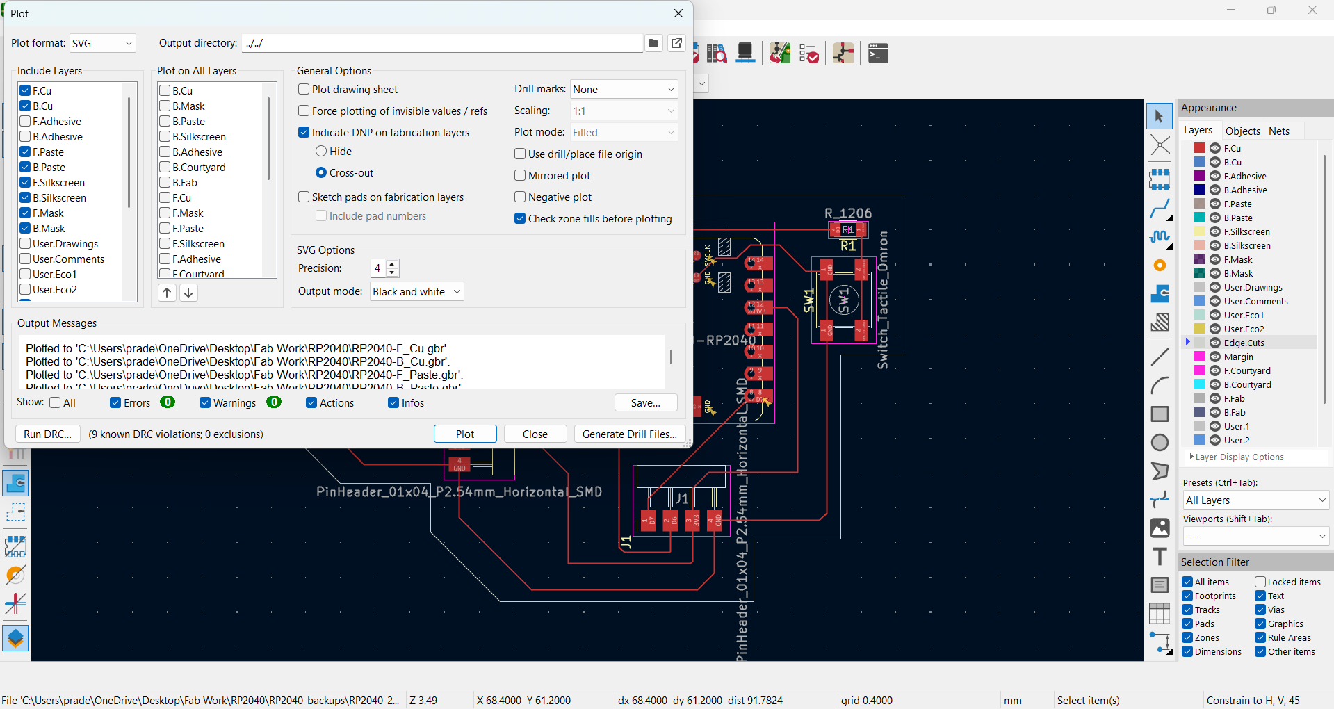
I exported the SVG files for further use in the fabrication process.
After confirming that all necessary layers were plotted, I saved the output files for future use.
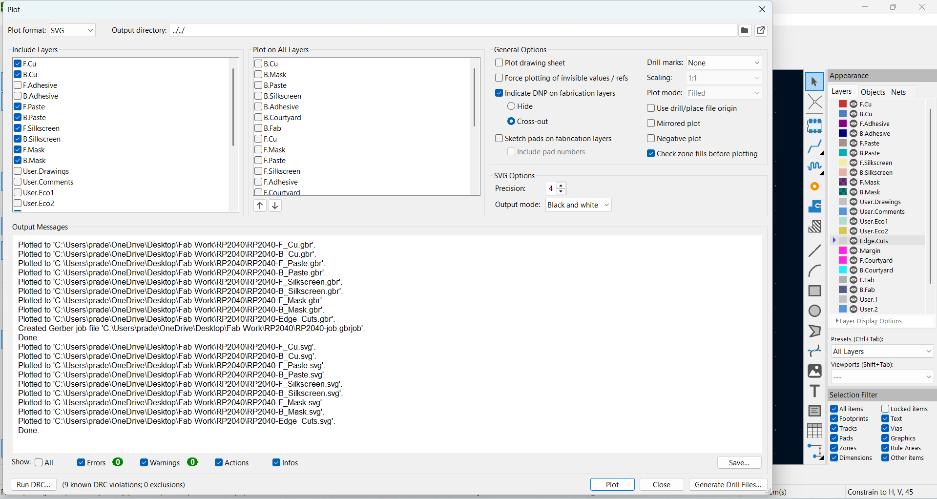
All output files were saved in the project folder for future reference and fabrication needs.
SVG format of the PCB design was successfully generated.

The Edge Cut SVG format was also prepared for final output.
| Pin | Connected To | Description |
|---|---|---|
| D0 | Switch SW1 | Input |
| D1 | LED D1 | Output |
| D6 | Header J1 Pin 2 | Debug/External IO |
| D7 | Header J1 Pin 1 | Debug/External IO |
| D2, D3 | Header J3 | Extra GPIO / Debug |
| D4, D5 | Header J2 | Extra GPIO / Debug |
| 3V3 | All Headers | Power Output |
| GND | All Headers | Common Ground |