Learning Experience
Throughout this assignment, I gained extensive hands-on experience in system integration, PCB design, embedded programming, 3D design, and product testing, including both hardware and code. I deepened my understanding of phototransistor sensors and successfully worked with the ATtiny1614 microcontroller. Additionally, I learned how to power and control devices using solar energy, which enhanced my knowledge of sustainable energy applications. I also explored multiple digital fabrication techniques, including 3D printing, which further enriched my practical skills in prototyping and product development.
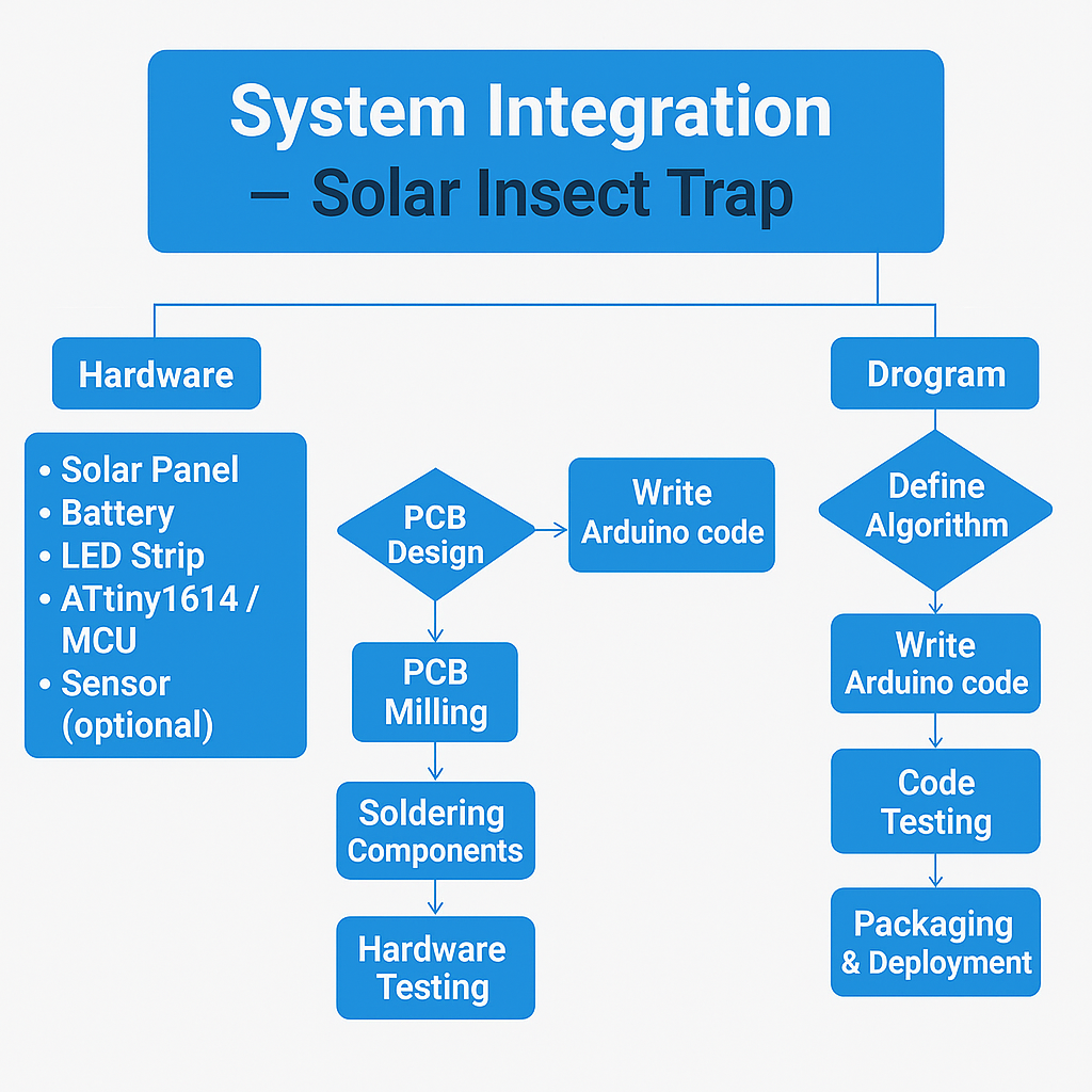
Task: System Integration
Individual project:
Design and document the system integration for your final project
System Integration refers to the sophisticated process of combining multiple independent sub-systems or components into a single, cohesive, and fully functional system. The primary goal of this process is to ensure that all individual elements, whether hardware or software, operate together harmoniously to deliver optimal performance and efficiency. In the realm of information technology, system integration typically involves the seamless unification of computing hardware, software applications, networking infrastructure, and data storage solutions. This integration enables disparate systems—often developed by different vendors—to communicate, exchange information, and function as a unified environment. By eliminating data silos and reducing redundancy, system integration streamlines operations, enhances workflow efficiency, and significantly improves data accessibility across the organization. Moreover, it plays a vital role in enabling real-time data sharing, process automation, and informed decision-making. In today’s rapidly evolving digital landscape, effective system integration is essential for achieving operational agility, supporting enterprise-wide innovation, and driving successful digital transformation initiatives.
About the Solar Insect Trap
An environmentally friendly and solar-powered device, the solar insect trap is designed to attract and capture flying insects using light. This innovative solution specifically targets harmful agricultural pests such as thrips, mites, whiteflies, and red spiders, which are known to cause significant damage to crops. By reducing the dependence on chemical pesticides, these traps offer a sustainable and eco-conscious alternative for pest control, helping to preserve soil health and protect biodiversity.
Detailed Component List for the Solar Insect Trap
This section provides a comprehensive and well-organized list of all the materials and electronic components used in the development of the Solar Insect Trap project. Each item included plays a vital role in ensuring the effective functioning and sustainability of the device.
| Sr. No. |
Item |
Specification & Description |
Quantity |
| 1 |
Solar Panel |
6V, 1–3W; used to charge the battery from sunlight. |
1 |
| 2 |
Rechargeable Battery |
Li-ion, 3.7V – 2000mAh; powers the LED and other components during the night. |
1 |
| 3 |
LED Strip (White Light) |
4V white light strip to attract insects at night. |
1 |
| 4 |
Charge Controller Module |
Manages solar charging and protects the battery from overcharging or discharging. |
1 |
| 5 |
Phototransistor Sensor |
Detects light levels and automatically turns the LED on or off. |
1 |
| 6 |
Trap Container / Jar |
Transparent or semi-transparent box where insects are collected. |
1 |
| 7 |
3D Printed / Plastic Casing |
Outer body or enclosure for mounting all components securely. |
1 |
| 8 |
Connecting Wires |
Used for internal wiring between all electronic components. |
As required |
| 9 |
PCB (Printed Circuit Board) |
Board for assembling the sensor, microcontroller, and LED circuitry in an organized way. |
1 |
| 10 |
Microcontroller (Optional) |
ATtiny1614 – used to process sensor data and control the system intelligently. |
1 |
Testing the Electronics – Sensor and Code Validation
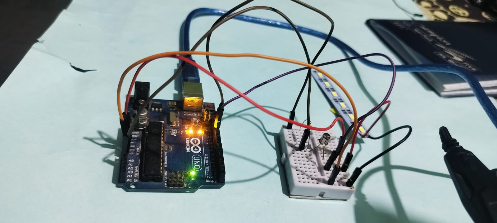
To ensure the proper functioning of my sensor and to identify the required components for final implementation, I conducted a basic electronics test. This helped me in understanding the behavior of the phototransistor and LED control, which will support me in designing an effective PCB circuit.
Components Used for Testing:
- Arduino – Used as the microcontroller for testing input/output logic.
- Phototransistor Sensor – To detect ambient light and simulate day/night conditions.
- LED – Used as output to verify if the light detection works correctly.
- Jumper Wires – For temporary circuit connections.
- 10kΩ Resistor – Used as a pull-up resistor with the phototransistor for voltage division.
Purpose of the Test:
- To check whether the phototransistor correctly responds to light changes.
- To test if the LED turns ON/OFF based on sensor readings.
- To confirm threshold levels and logic for programming.
- To get clarity on component placement and values for PCB design.
- To ensure compatibility with Arduino/ATtiny programming logic.
🔗 Connection Diagram – For Testing Purpose
The following connections were made to test the functionality of the phototransistor sensor and LED using an Arduino:
- A0 (Analog Pin) → Connected to the sensor data pin
- 10kΩ Resistor → Connected between sensor data pin and GND (acts as a pull-down resistor)
- 5V → Connected to the VCC pin of the sensor
- Digital Pin 12 → Connected to the LED positive leg (anode)
- LED negative leg (cathode) → Connected to GND via a resistor
This setup allows the Arduino to read light levels from the phototransistor and turn the LED ON or OFF based on ambient light conditions.
Arduino Code for Phototransistor LED Test
int sensor = A1;
int ledPin = 12;

void setup() {
  Serial.begin(9600);
  Serial.println("Phototransistor test");
  pinMode(ledPin, OUTPUT);
}

void loop() {
  int war = analogRead(sensor);
  Serial.print(war);

  if (war > 200) { // If value is above 200, turn on LED
    Serial.print(" LED lit");
    digitalWrite(ledPin, HIGH); // Turn on LED
  } else {
    digitalWrite(ledPin, LOW); // Otherwise, turn off LED
  }

  Serial.println("");
  delay(200); // Wait for 200 milliseconds
}
My final product code functioned smoothly, and the Arduino Uno board operated without any issues. At this stage, all that remained was to test the code and verify the performance of the connected sensors.
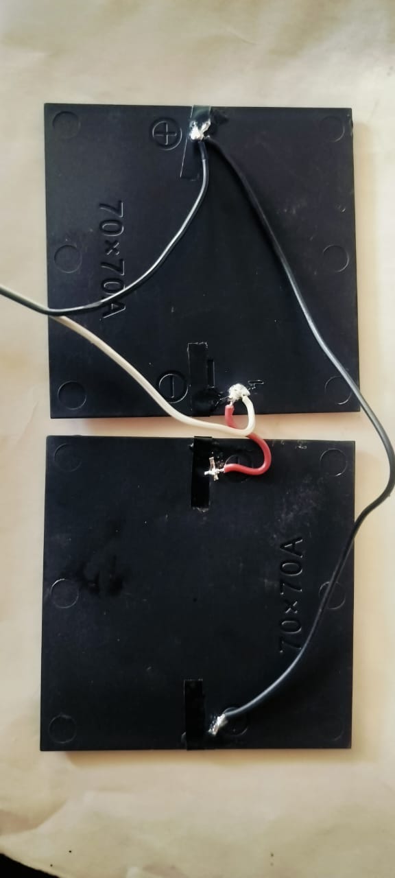
>After successfully testing the code, I selected two solar panels, each rated at 6 volts and 0.5 amps. I then soldered both panels together in parallel by connecting the positive terminals to each other and the negative terminals likewise. As a result of this parallel connection, the combined output of my solar panel system remained at 6 volts, while the current increased to 1 amp.
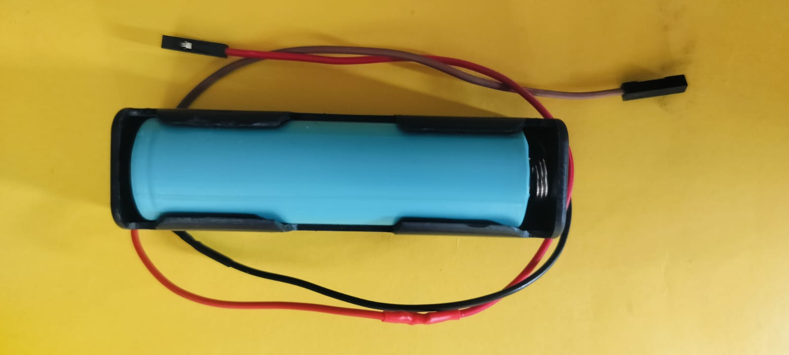
I used a 3.7V 2200mAh rechargeable battery and securely placed it inside the casing holder. The battery wires were carefully soldered to ensure a strong and reliable electrical connection
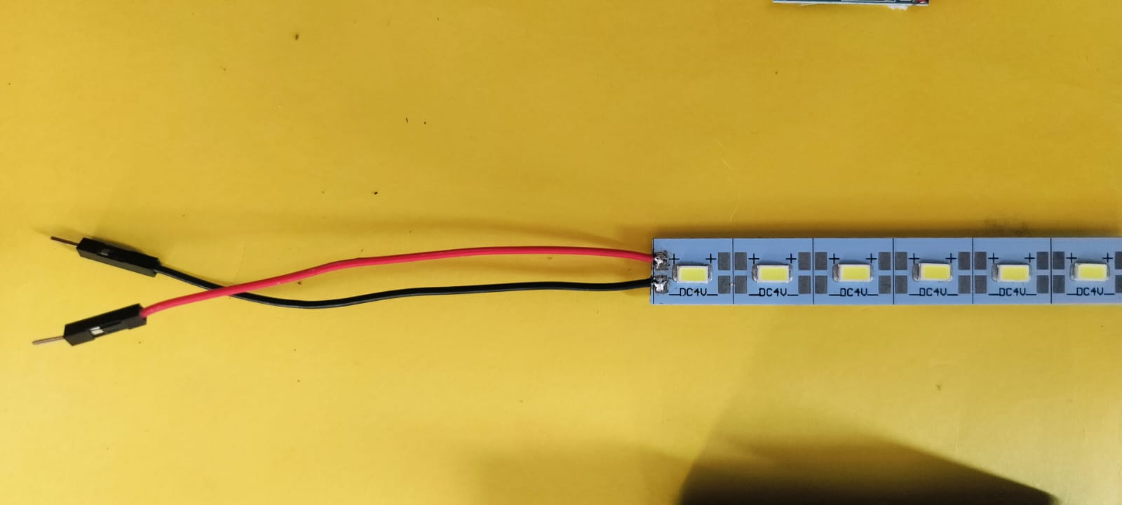
I selected an LED strip, and carefully soldered jumper wires to the positive and negative terminals of the LEDs to ensure a secure electrical connection.
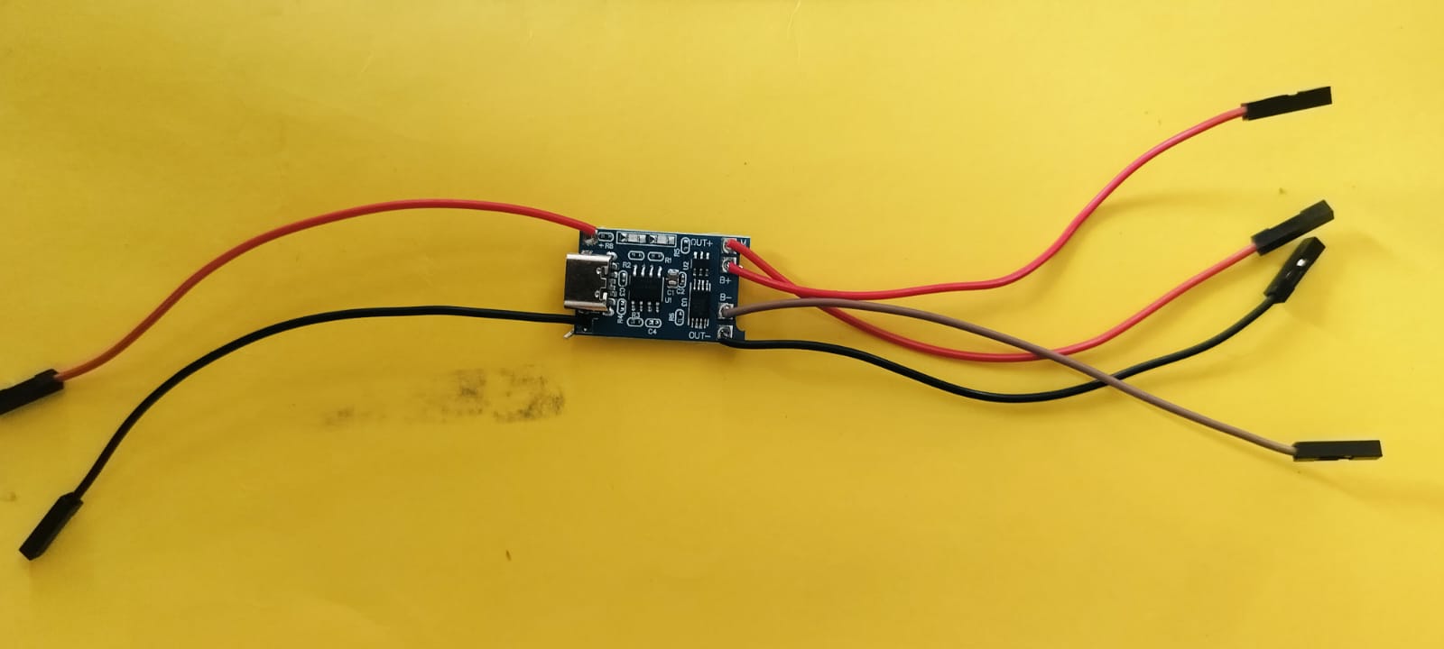
Finally, I used the TP4056 charging module. First, I carefully soldered the wires coming from the solar charging panel to the input terminals of the module. After that, I soldered the battery input wires to ensure proper connection for charging. Lastly, I connected and soldered the two output wires that will supply power to the connected load or device.
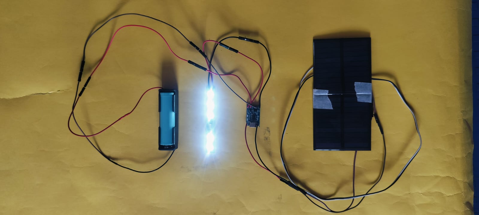
I connected all the components together, including the battery, solar panel, and charge controller. I carefully joined all the wires and ensured proper connections between each part. After completing the setup, I conducted a thorough test to confirm that all the soldered components were functioning correctly.
This video demonstrates the testing of all components integrated into the project, showcasing their functionality and performance.
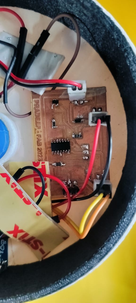
PCB Design Process Using ATtiny1614
To design my PCB, I used the ATtiny1614 microcontroller, which is compact, efficient, and suitable for low-power embedded systems. Below is a step-by-step overview of my PCB fabrication process
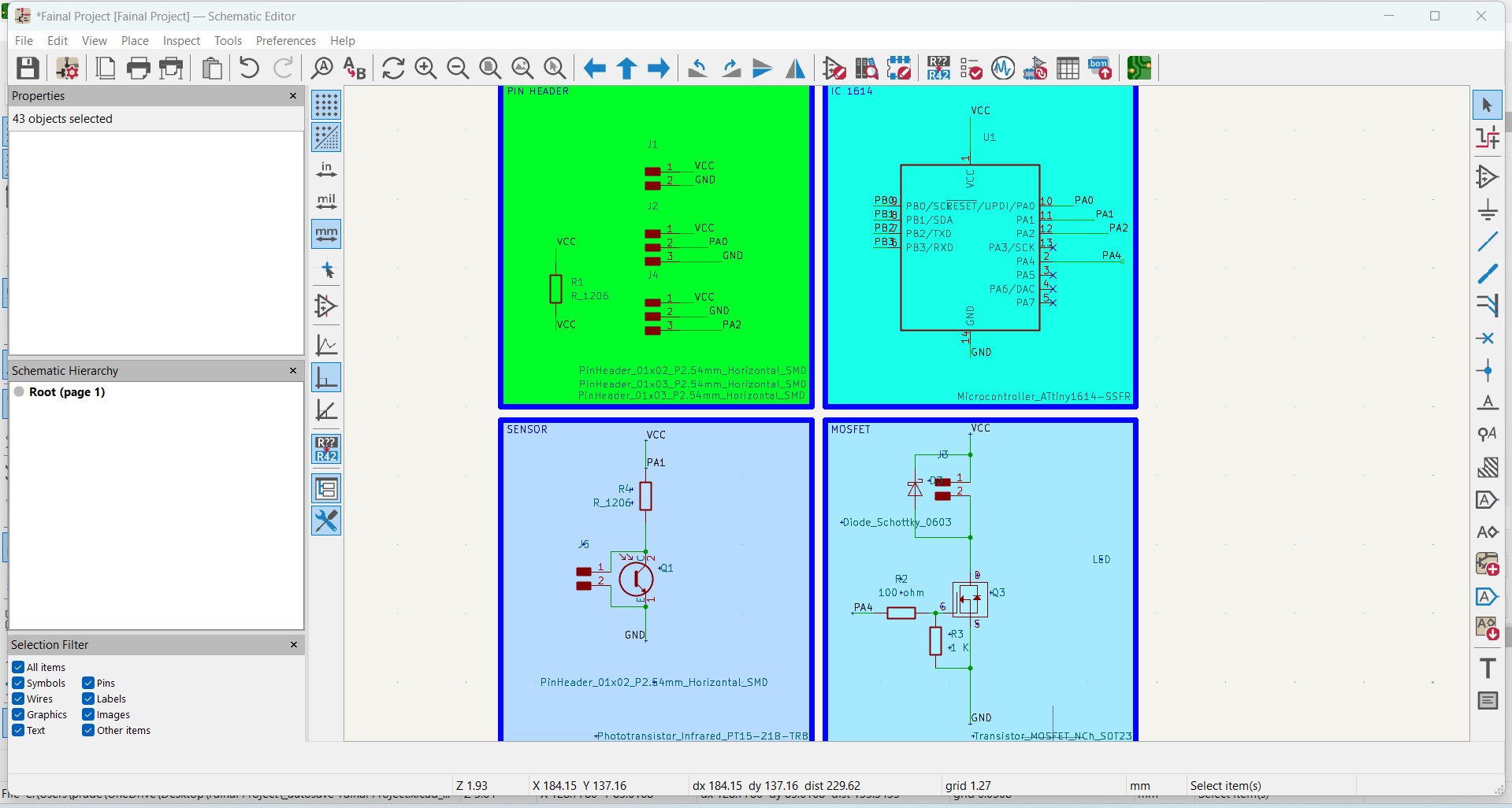
1. Created the Schematic Diagram:
I began by designing the complete schematic diagram of my circuit using KiCad. This step helped define all the electronic connections and components required.
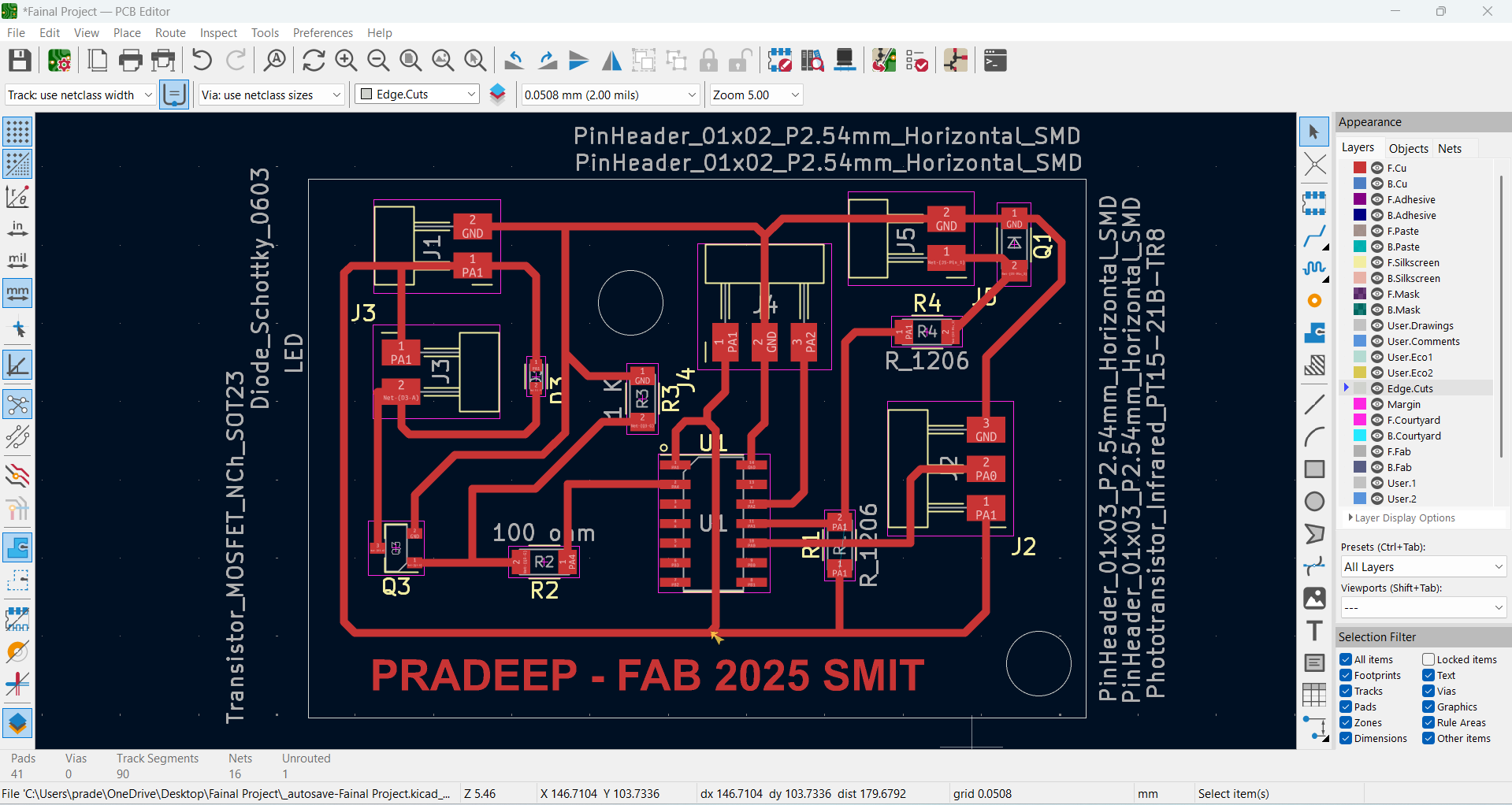
2. Performed PCB Routing in PCB Editor:
After finalizing the schematic, I moved to the PCB Editor to perform routing. I carefully routed all signal paths to avoid overlaps and ensured clean and efficient layout connections.
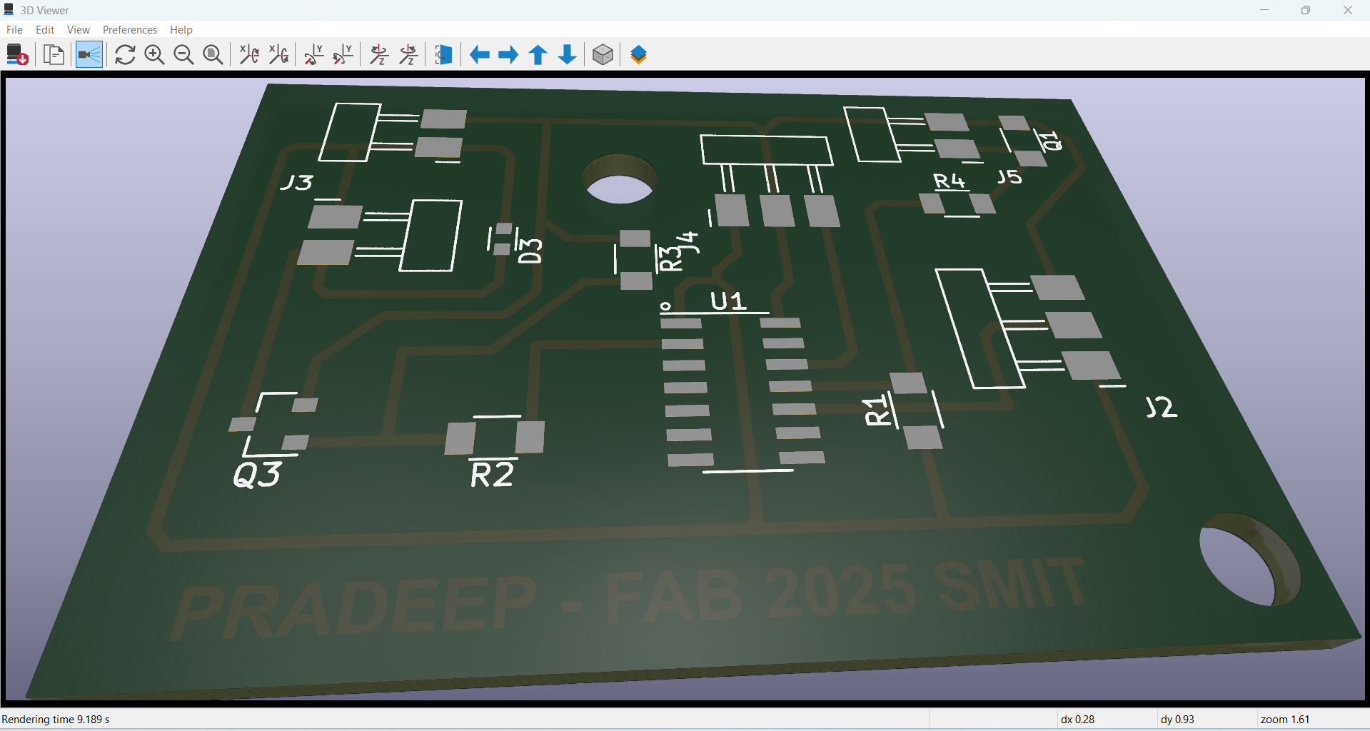
3. Viewed the 3D PCB Model:
Once the routing was complete, I generated a 3D view of the PCB. This allowed me to visually inspect component placements and ensure there were no conflicts or alignment issues.
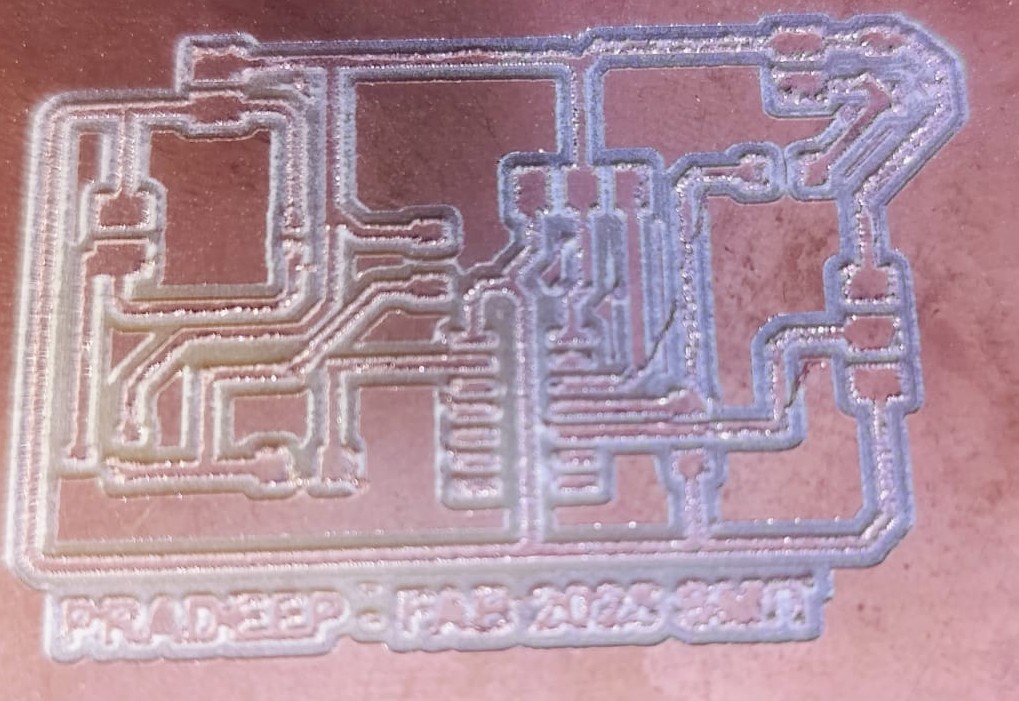
4. Performed Tracing with SRM-20 CNC Machine:
I used the SRM-20 CNC milling machine to trace the PCB layout onto the copper-clad board. The tracing process precisely carved out the paths required for the circuit.
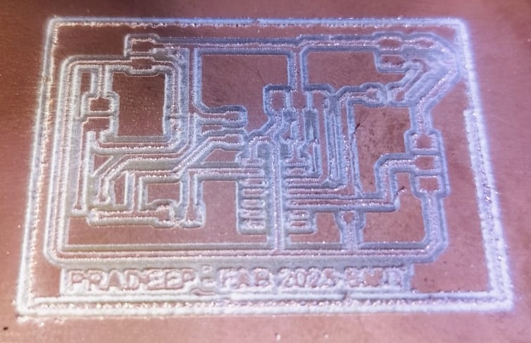
5. Applied Edge Cutting for Board Shaping:
To give the PCB its final shape and size, I used the edge-cutting feature. This step ensured the board was trimmed neatly and fit perfectly into its enclosure.
6. Applied Soldering Paste and Soldered the IC:
I applied soldering paste onto the PCB pads and then carefully placed and soldered the ATtiny1614 IC using a soldering iron.
7. Soldered All Components to Complete the PCB:
Finally, I soldered all the remaining components onto the board. After checking all connections, my PCB was successfully completed and ready for testing.
Component list
ATtiny1614 IC
2× LED Pin Header
Phototransistor Sensor Pin Header
3-Pin Header for UPID
3-Pin Header for Extra Sensor
Resistor (10KΩ, 100Ω)
Diode
MOSFET
Final Product Design Thought Process
In the final stage of my project, I focused on designing the product with a clear vision. I carefully considered the manufacturing process and decided that most of the components should be 3D printed to ensure precision and ease of assembly. Some parts, however, were better suited for laser cutting due to their flat profiles, while others required the durability and strength provided by wood routing. Based on these considerations, I began designing the product accordingly.
My goal was to create a compact and cost-effective solution that could be mounted on a light pole or any standard vertical support structure. I aimed for a design that would be lightweight and aesthetically minimal, making it easy to install in polyhouses, farms, or any outdoor environment without requiring complex infrastructure.
I designed all these components using SolidWorks, ensuring each part was accurately modeled according to the functional and manufacturing requirements of the final product.
Cable Routing and PCB Installation
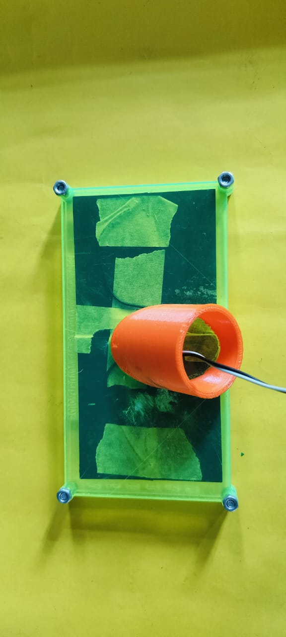
1. Solar Panel Wiring
I designed a round pipe at the back of the solar panel through which the wire is routed to the charge controller. This setup ensures the wiring is safely enclosed and protected.
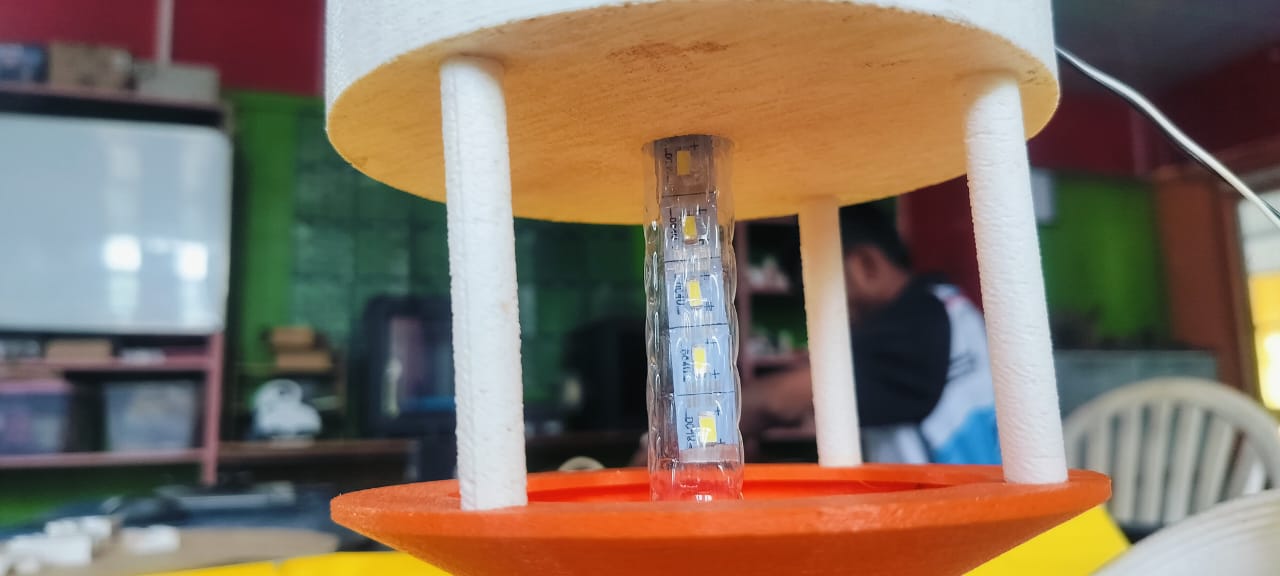
2. LED Wire Management
I provided an 18 mm hole in the enclosure box, which perfectly fits the LED diffuser. The same hole is used to neatly route the LED wire inside.
3. Wiring of Other Components
The wiring of all other components is organized inside the enclosure box. I used jumper wires and secured them in place using double-sided tape and hot glue (Fevistic) to keep the wiring clean and stable.
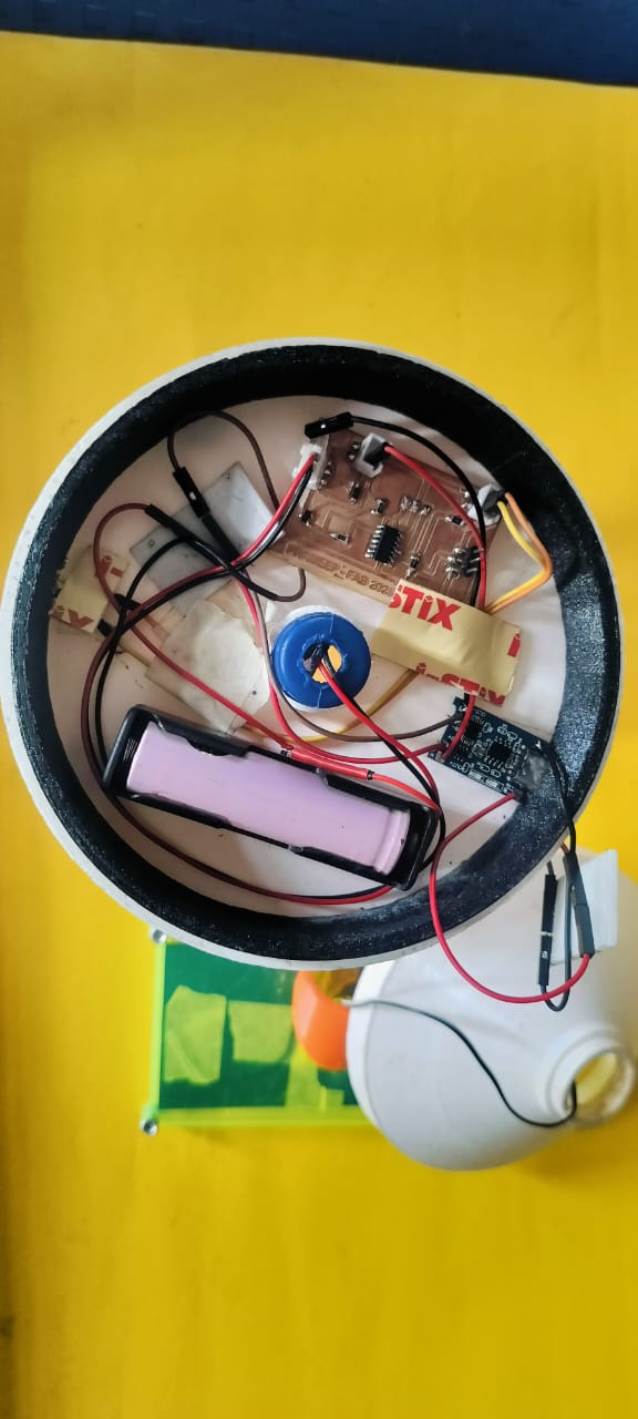
4. PCB Installation
The PCB is also fixed inside the enclosure box using double-sided tape and hot glue, ensuring it stays firmly in place without any movement.