
Assignments
Group Assignment
- Characterize the design rules for your in-house PCB production process
- Submit a PCB design to a board house
Individual Assignment
- Make and test a microcontroller development board that you designed
- Extra credit: make it with another process
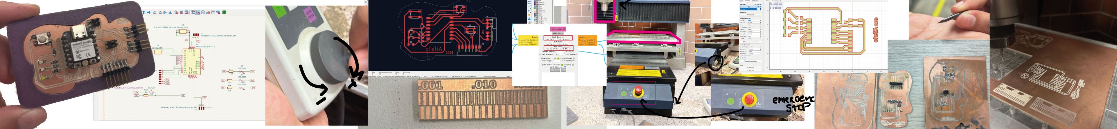
GROUP ASSIGNMENT
More specific detailed from the worked done with Ernesto Castro in Fab Lab Universidad de Lima here
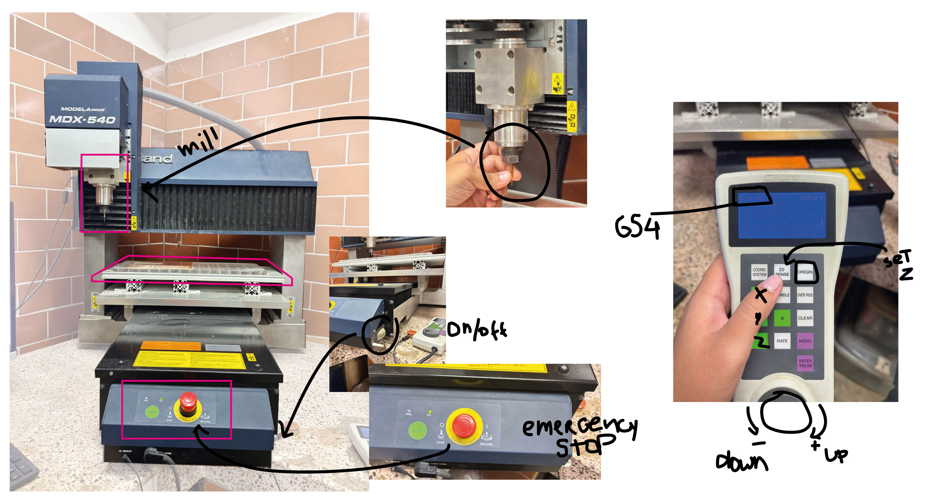
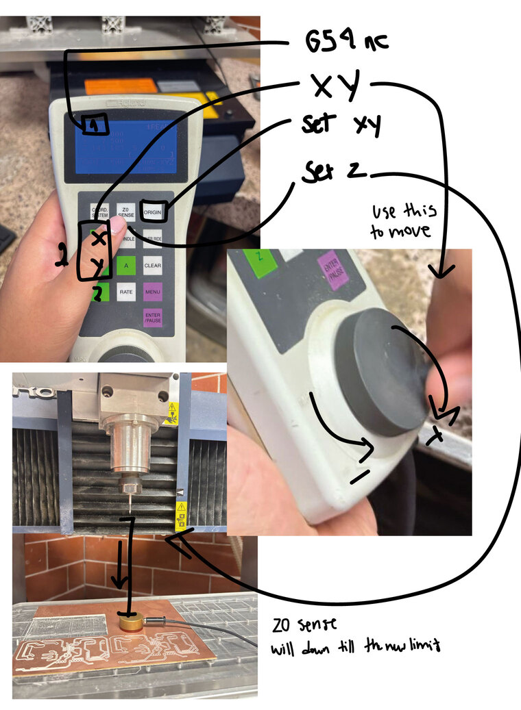
R O L A N D modela pro M D X - 5 4 0
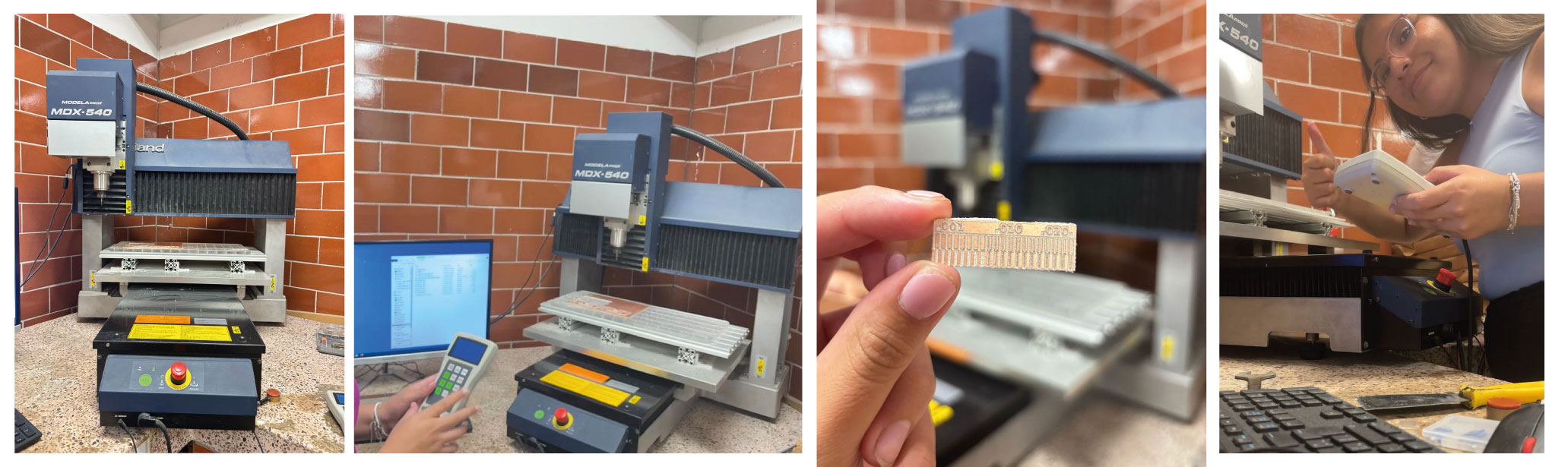
Setting the Modela pro MDX-540
The machine we have in the fablab Ulima is the Roland Modela pro MDX-540 First we have to calibrate the workspace and material. Keeping in mind that the cut will start in the first quadrant and cut from bottom to top and to the right.
SETTINGS
So, to start using the machine, first we have to change the mill, set the origin for the mill and calibrate the Z axis before running the software to start.
SETTINGS
g r o u p T E S T S
First to generate the gcode, we import the PNG file to MODS. And set the option for raster andthen for cut mill.
SETTINGS for MODS
INDIVIDUAL ASSIGNMENT
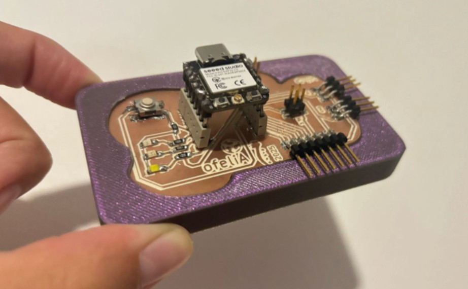
solding PCB final test with a 3d printed case.
d e sign the B O A R D
I redesign the board I made in week 6 in KiCad because I forgot to leave some free pins to connect and try more components in the future. I kept the button and the leds. But change for 3 leds from white to orange to red as I want my final project to have a color palette. I left 5 extra pins with all the connections a RGB led needs and also some free GND, 5V, 3.3V and analog pins.
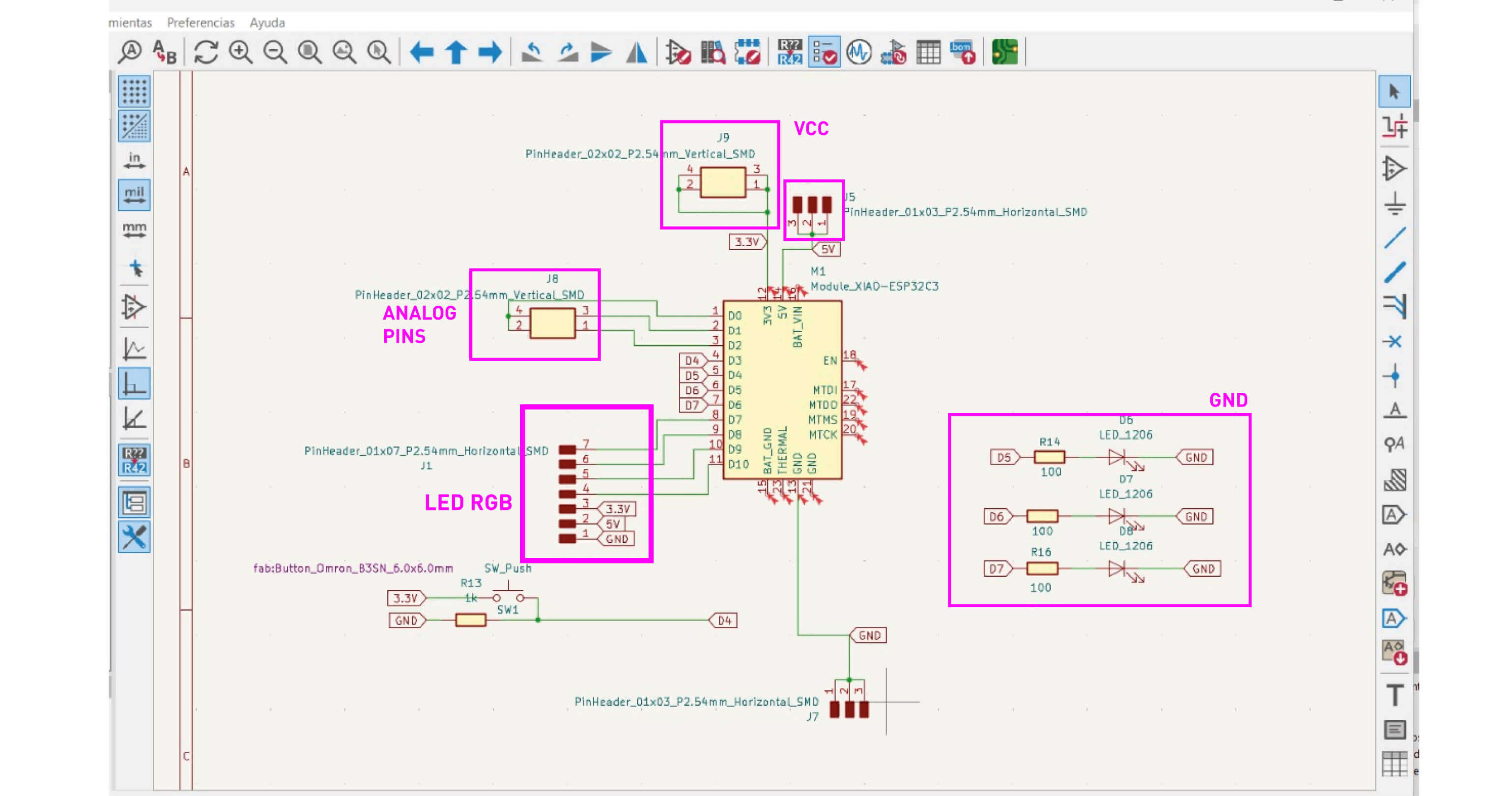
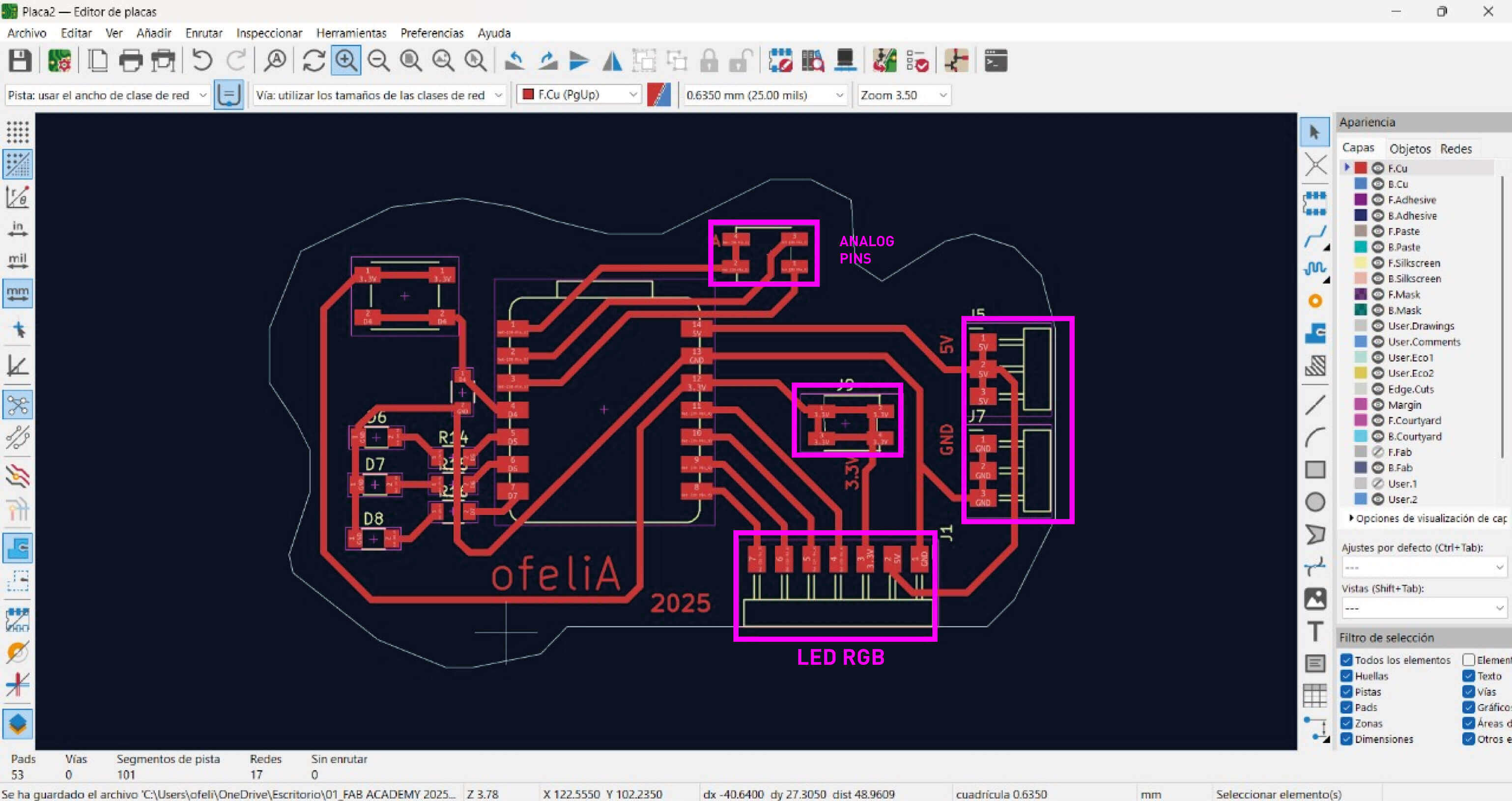
KiCad redesign
I had to update the footprint of some components exactly for the ones I had. Because I wanted to try new components appart from pin headers.
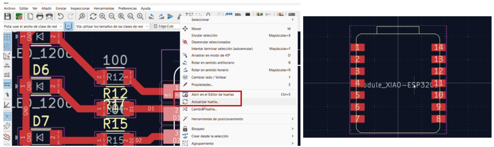
Update a footprint
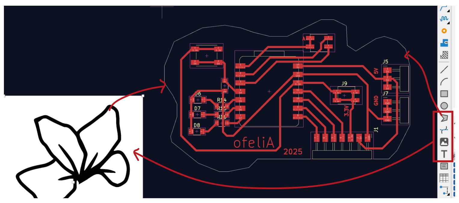
For the contour I wanted to make and organic shape following my drawings of nature. However the best I could make was to upload a reference picture and make the contour as a polygon with the bezier tool.
width roads
F L A T C A M
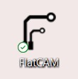
For the individual assignment I also tried FLATCAM. I download from here. I exported the .gerbr file from Kicad and generated the G code from setting the mill options. First It will generate the routing and then the CNC object so after this settings finally generate de cnc code for the machine.
First move the gerber lines to the center axis. Then Isolate routing.
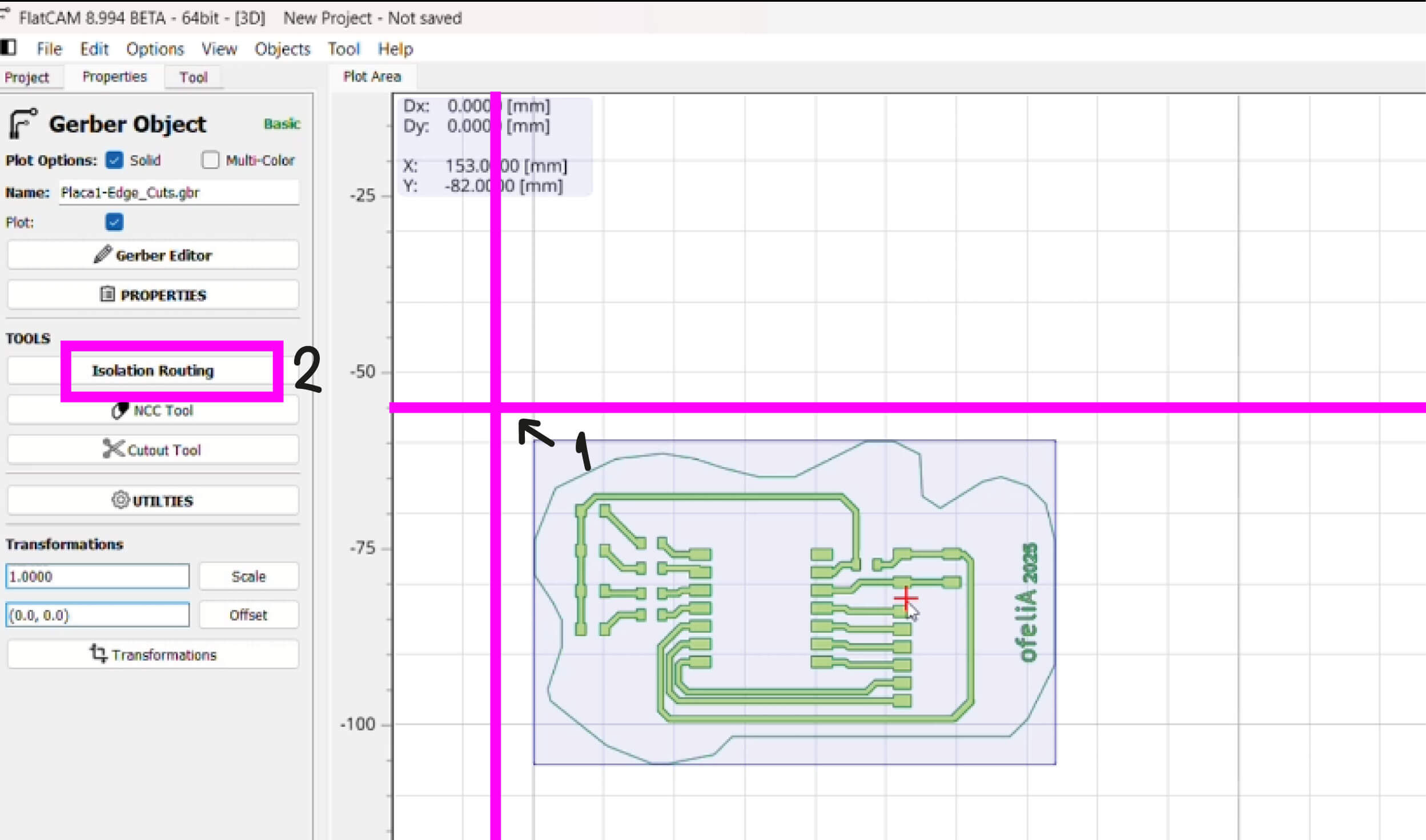
Then set the diameter tip from the tool, the angle and make sure to change the spindle speed. Then generate the CNC object.
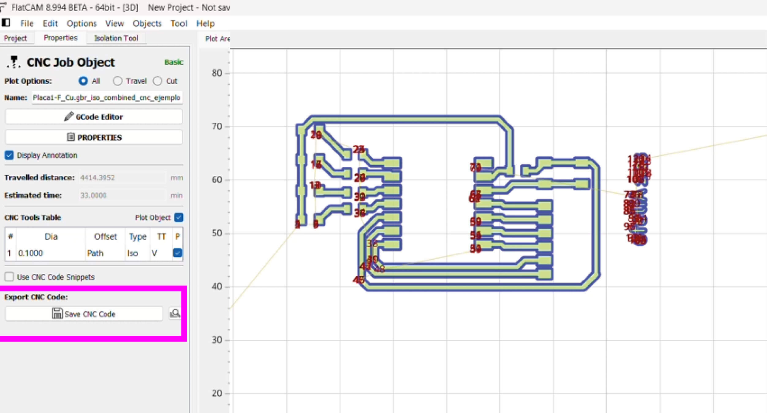
Finally save the CNC CODE.
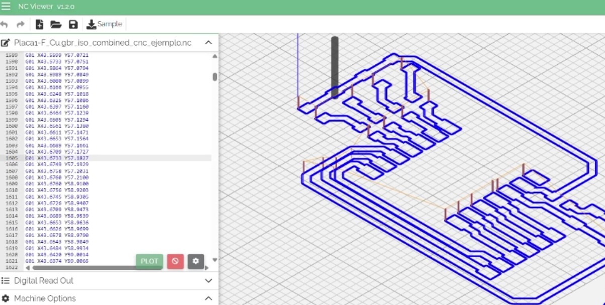
Before sending the code to the machine, I simulate the g code in https://ncviewer.com/ where I could see the layers of cut and if there is no extra dots from the board to delete.
Left png from kicad and right some drawings in Illustrator to have an organic edge.
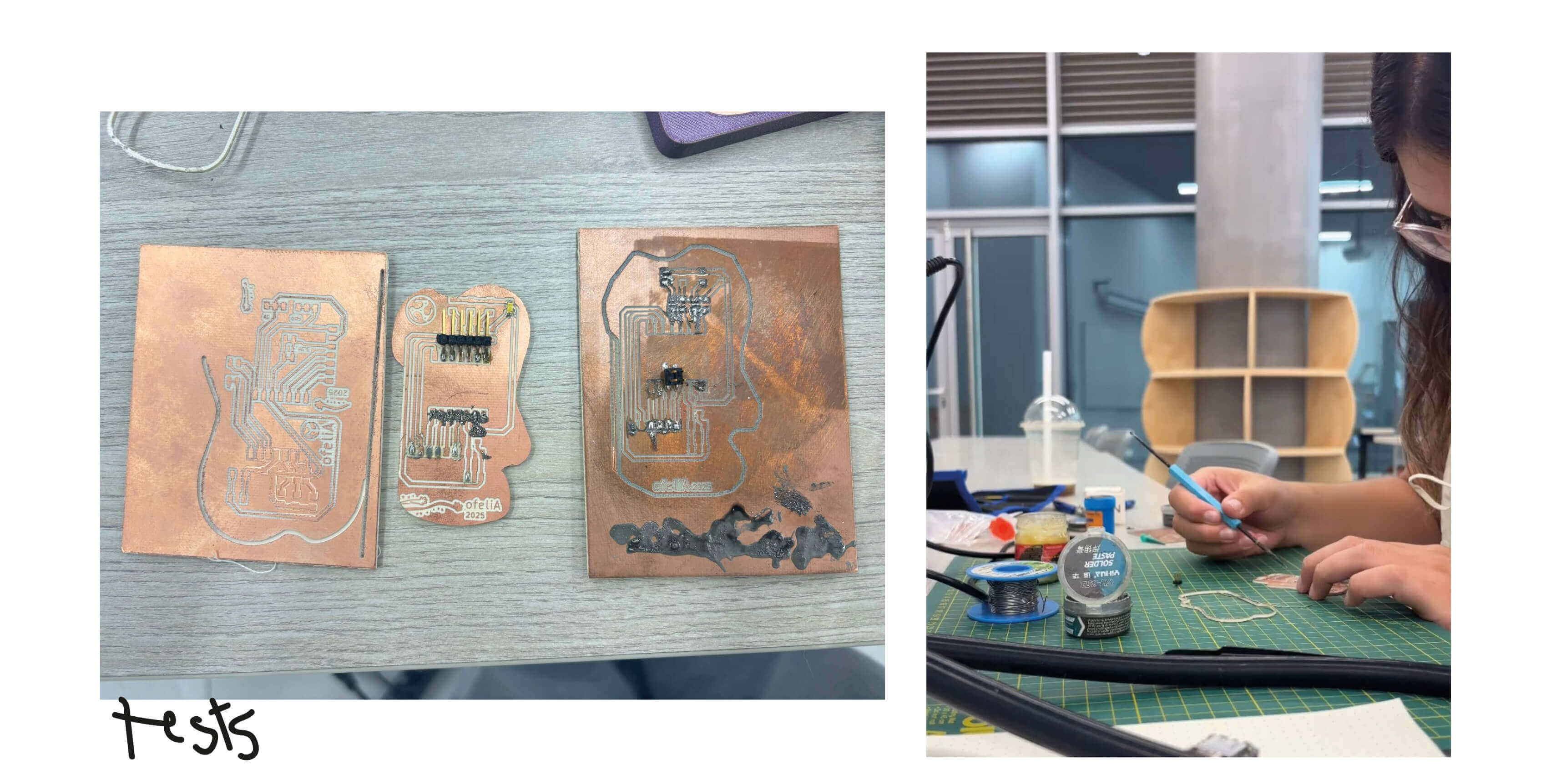
Fabrication test 1
I cut the first try in fiberglass because I wanted to try another material. However this is more toxic as it left a strange smell and cutting chip. Also with a mill of 0.8 that cut the tests in ceramic did not cut this material. Also i found the surface too rough. In this test I could manage to see if the text was in the correct layer and size to raster and it was. Also here is where my instructor and me realized that the space i left for the free pins to connect with another board will not work because it wasn't in the edge. So the other board will have to be upside down to fit. Also this free pins could not work because it also needed free GND and VCC pins to connect.
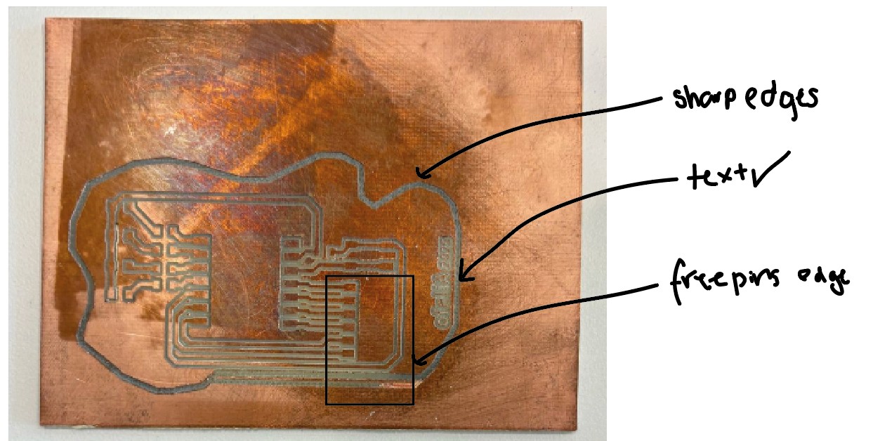
First try in fiberglass.
M O D S
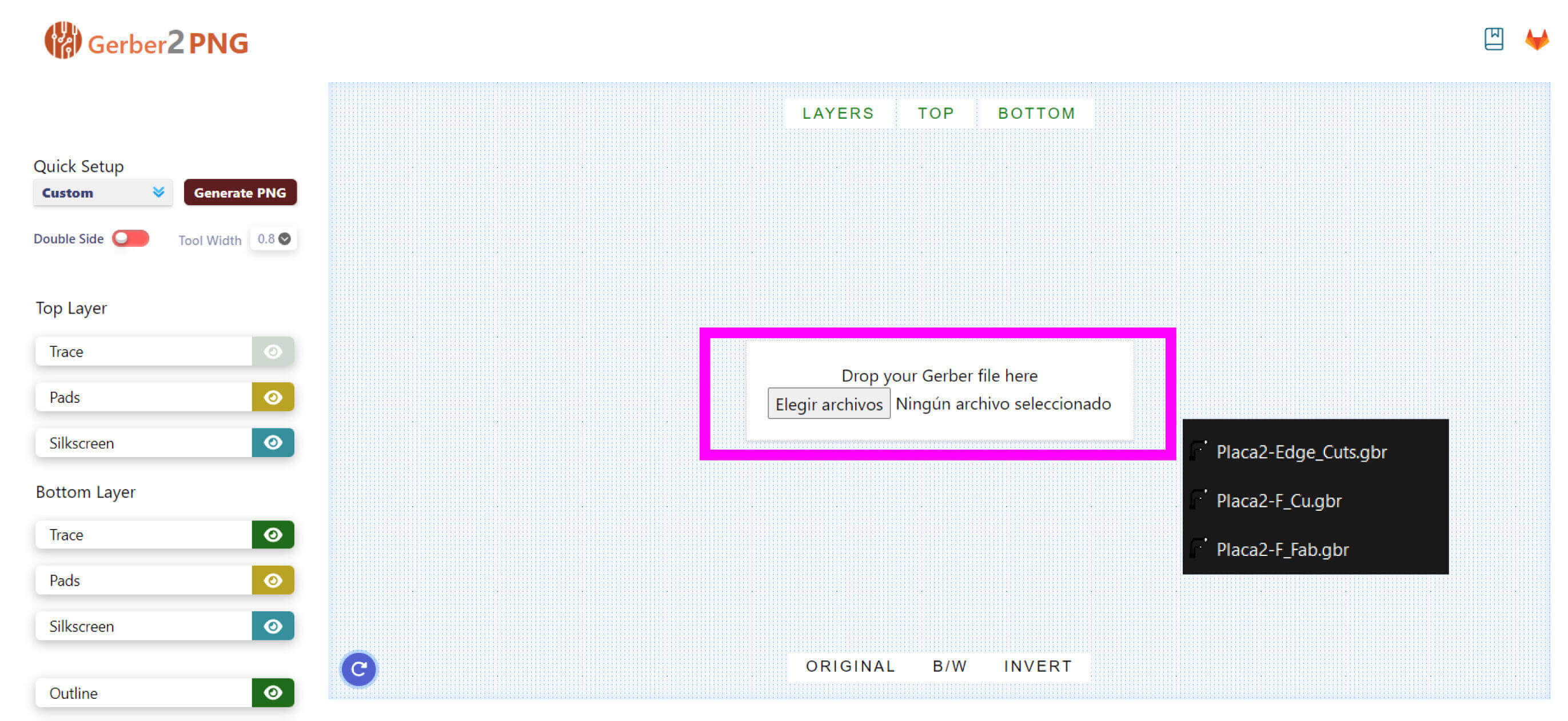
I didn't like the contour from kicad, and as MODS make the gcode from a PNG I exported the kicad gerber to Gerber2png and make a contour in Illustrator with the png in real size so it doesn't scale, and added some other drawings to personalize the board and test other figures.
Gerber to png
Import all the gerber files in order to work.
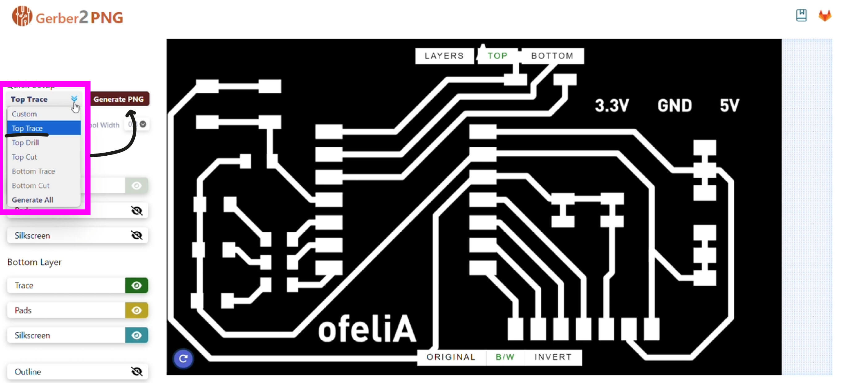
Make the top traces.
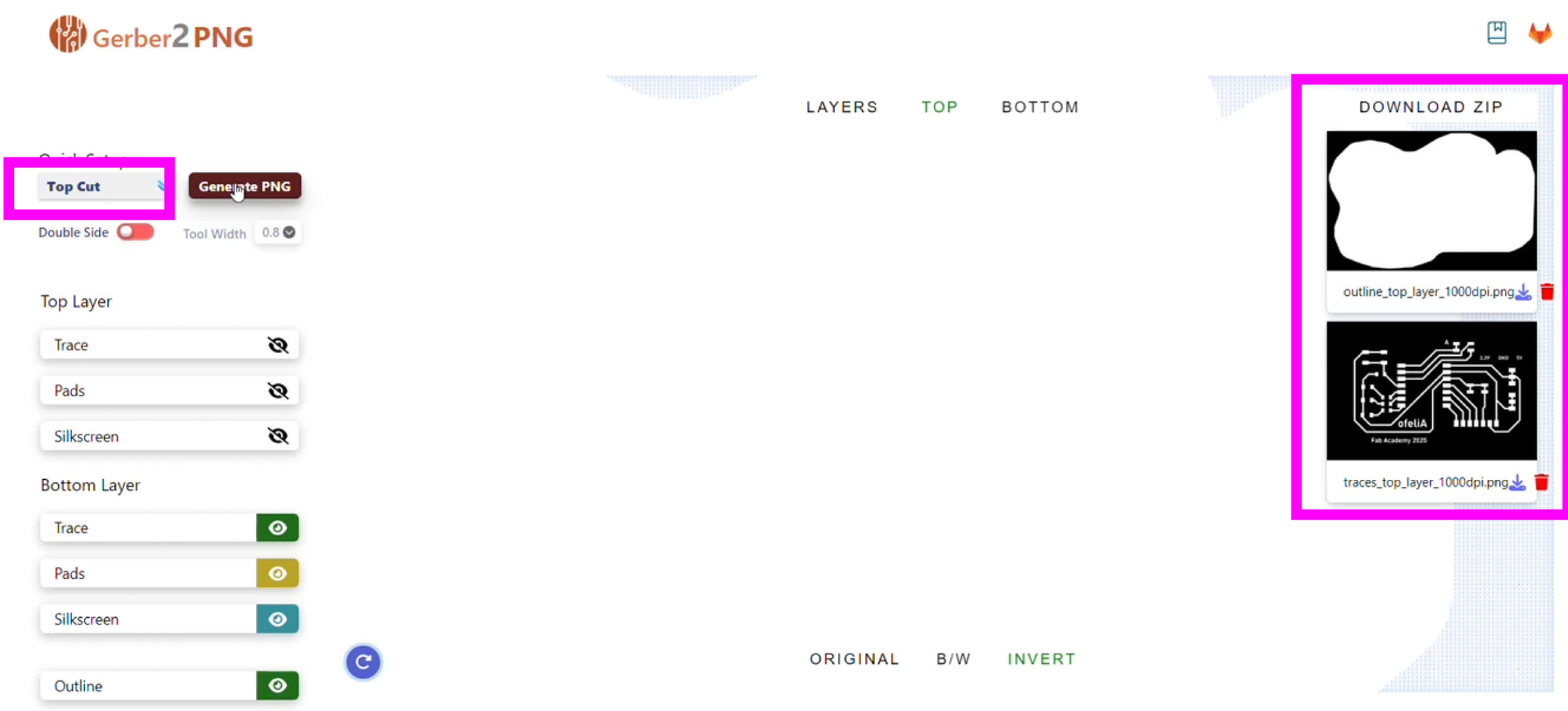
Make the cut border. The png will open in the right side.
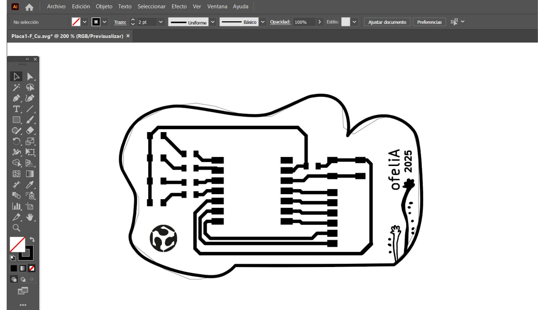
PNG imported in Illustrator and the final border and some drawings to try the detail.
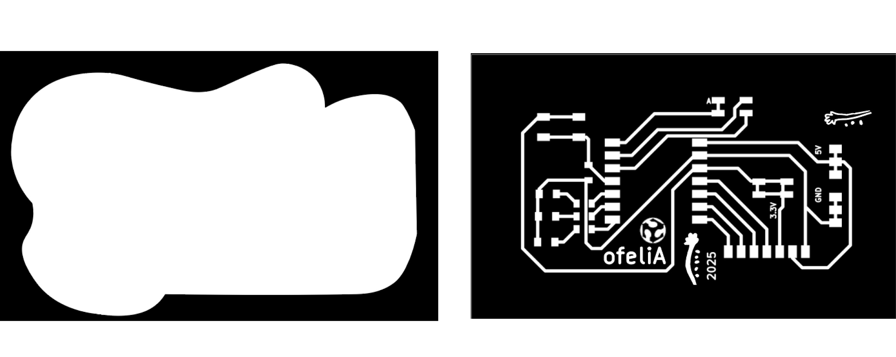
Final png.
Fabrication test 2
With the same settings from the group tests I sent the file in mods. However the first try of contour I forgot to update the pcb design and it cut the wrong file. But I realize I was sending the invert file of contour in mods and make the contour another road.
Final tests of contour.
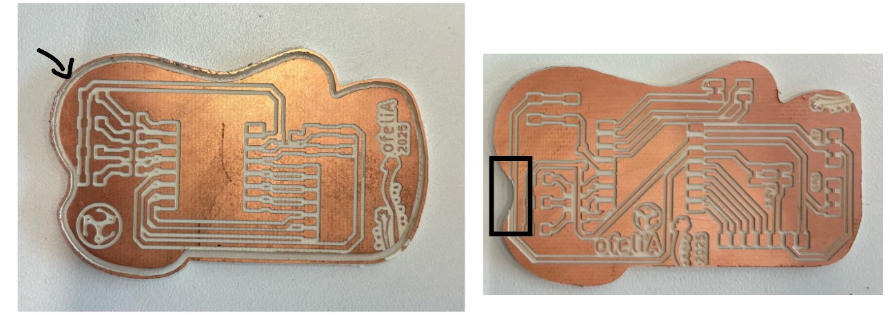
Then, I correct this inverting the contour as the image above, and make the correct edge BUT it somehow offset the cut and almost cut one road in the left. I tried to cut another one but the machine is in used and I will be cutting another one this weekend.
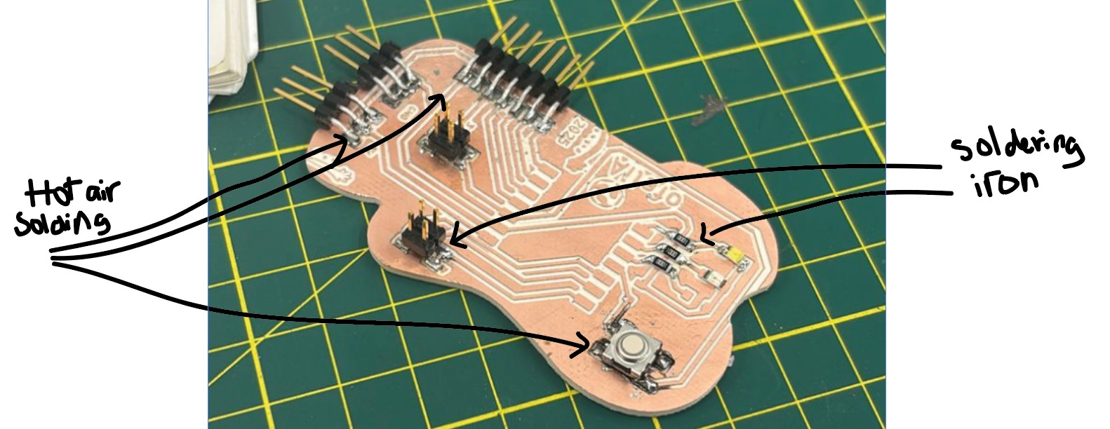
s o l d e r i n g my P C B
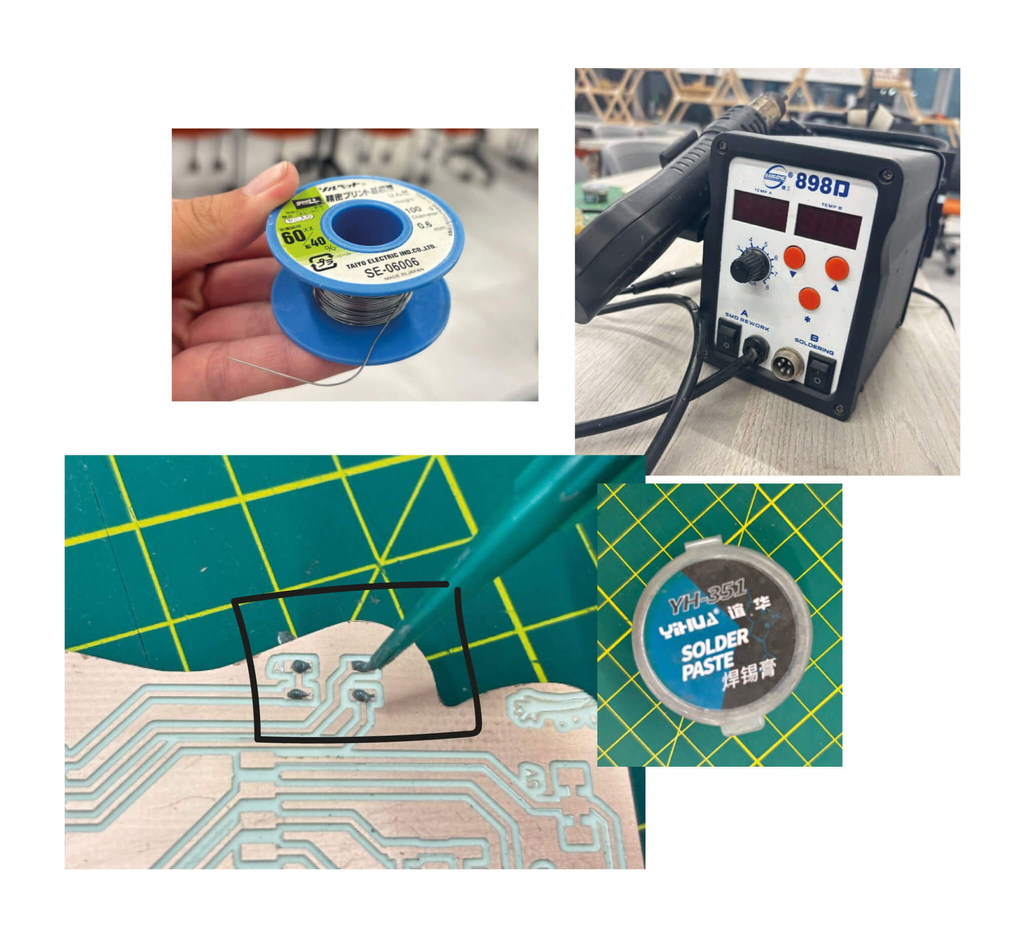
Soldering materials.
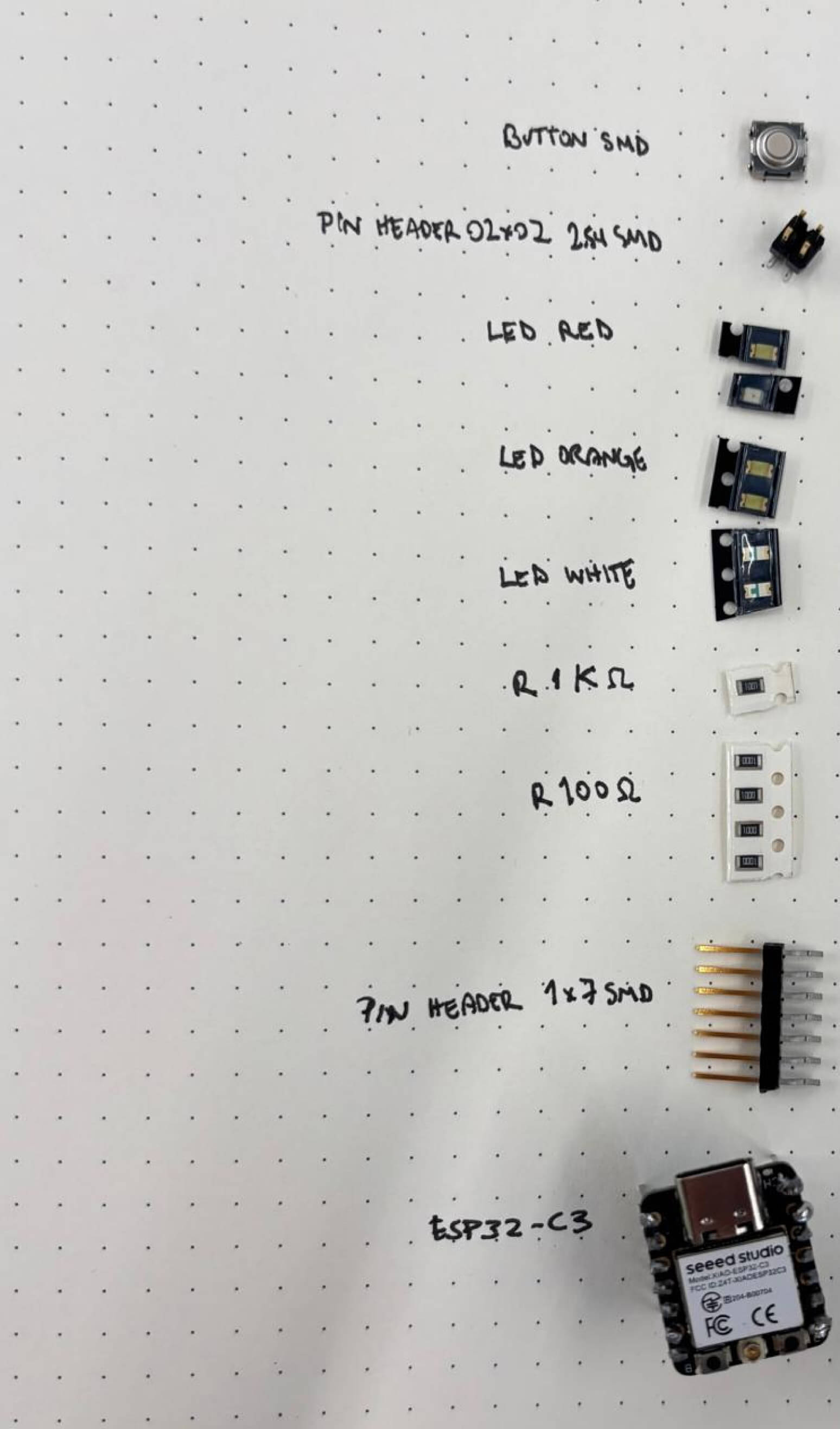
All the components
In the lab there was two options to sold. The soldering iron that I had used before and the hot air that works with a paste. I tried both and first makde some tests in the boards that were wrong. Once I felt confident I try with the paste first.
 You clearly can difference which are from the paste and which from the soldering iron. I found the paste very practical for long soldering but as it is liquidd it expands way too much with the air pressure and it is difficult to manage. I think this will be more easy if I clear all the pcb board and only left the roads.
Soldering tests with hot air and soldering iron
I tested the board with the multimeter to see if ther was continuity in the roads and If i made the soldering right before testing a promgramming code from week 4.
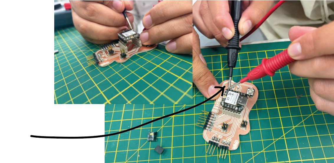
Testing continuity
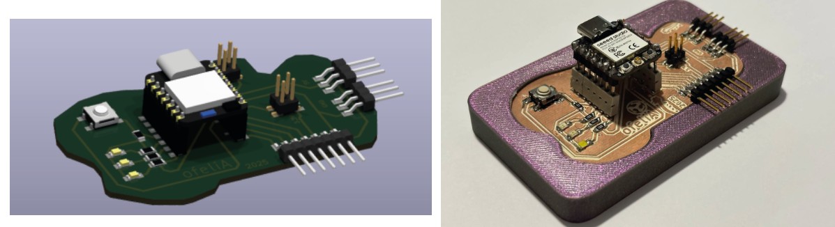
Kicad 3d preview
From also week 6 I design a case for the pcb board and printedit in PLA. I was very nervous it didnt fit as I had to make an offset because as I mention before the machine cut inside the edge contour and not in the axis. Making the board a little smaller.
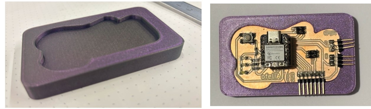
3D printed case for the board
I used the codes programmed in week 4 to turn on 3 leds by themselves within 1 second between each and then controlled by a button.
New try: Control the intensity of the led with a button.
This week I tried something new: to control the intensity of the leds by a button. I hd to search a lot between tutorials and some help of copilot to understand certain parts of the codes I found and finally made this wich I understood reads first the state of the button and counts the press and has some levels of color brightness if the button state changes.
const int LED1 = D4;
const int LED2 = D5;
const int LED3 = D6;
const int BOTON = D3;

int buttonState = 0;      // Estado actual del botón
int lastButtonState = 0;  // Estado anterior del botón
int pressCount = 0;       // Contador de presiones
unsigned long lastDebounceTime = 0;
unsigned long debounceDelay = 50; // Tiempo de antirrebote
int brightnessLevels[] = {0, 64, 128, 192, 255}; // Niveles de brillo
int currentBrightness = 0; // Brillo actual de los LEDs

void setup() {
  pinMode(LED1, OUTPUT);
  pinMode(LED2, OUTPUT);
  pinMode(LED3, OUTPUT);
  pinMode(BOTON, INPUT);
}

void loop() {
  int reading = digitalRead(BOTON);

  // Si el estado ha cambiado
  if (reading != lastButtonState) {
    lastDebounceTime = millis();
  }

  if ((millis() - lastDebounceTime) > debounceDelay) {
    // Si el estado ha cambiado y ha pasado el tiempo de antirrebote
    if (reading != buttonState) {
      buttonState = reading;

      // Incrementar el contador en la transición de LOW a HIGH
      if (buttonState == HIGH) {
        pressCount++;
        if (pressCount >= sizeof(brightnessLevels) / sizeof(brightnessLevels[0])) {
          pressCount = 0; // Volver al nivel más bajo
        }
        currentBrightness = brightnessLevels[pressCount];
        analogWrite(LED1, currentBrightness);
        analogWrite(LED2, currentBrightness);
        analogWrite(LED3, currentBrightness);
      }
    }
  }

  lastButtonState = reading;
}