
Assignments
Group Assignment
- Use the test equipment in your lab to observe the operation of a microcontroller circuit board
Individual Assignment
- Use an EDA tool to design a development board that uses parts from the inventory to interact and communicate with an embedded microcontroller
- Try another design workflow
- Design a case around your design
GROUP ASSIGNMENT
More specific detailed from the worked done with Ernesto Castro in Fab Lab Universidad de Lima here
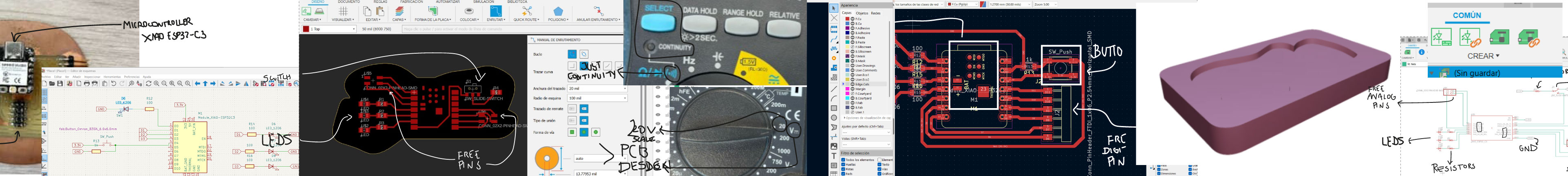
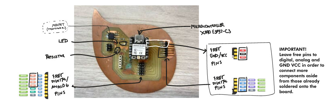
XIAO ESP32-C3 circuit board
development board example
We first used a development board made by Ernesto Buendia from Fab Academy 2024 week 9 to understand the circuits and measure the voltage and understand the polarity that we knew how to programm but not how it works in a circuit.
UPDATE from week 8: The free pins are important to connect more components aside from the ones alredy soldered in the board. And the free digital or analog pins needs also another GND and VCC free pins since every component needs one separated. So, at least leave 3 from each.
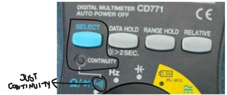
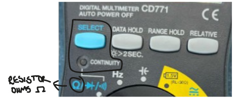
Our Instructor left us some assignments to test in the board:
- Continuity: Which pin corresponds to which pin on the microcontroller ☑
- Resistance: The value of the resistors on the board example ☑
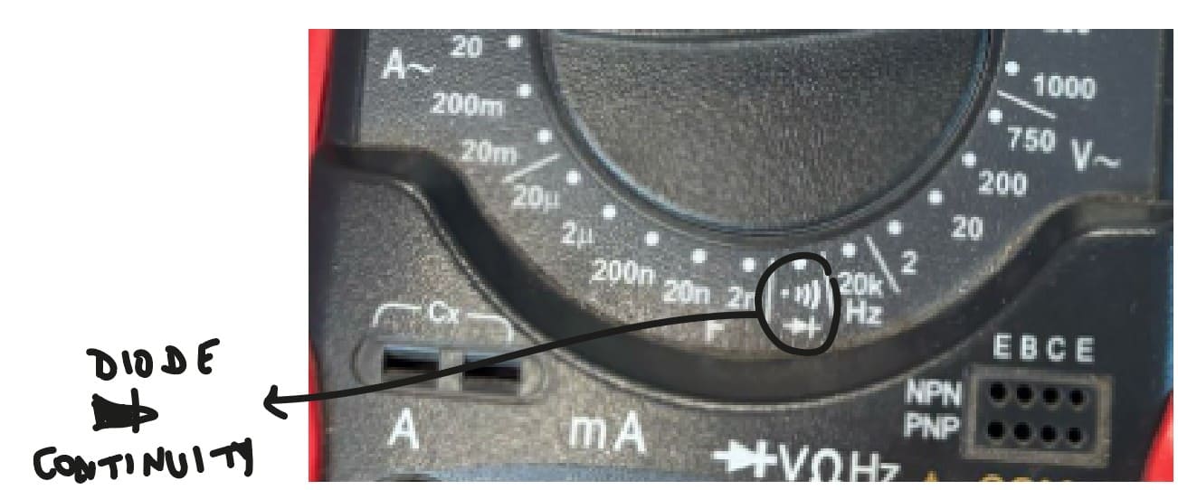
- Diode Test: To know the polarity. Anode and cathode ☑
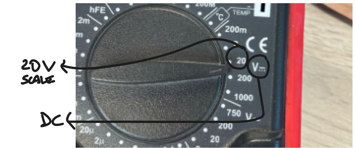
- Voltages: 1. LED with a digital signal, and 2. The LED with a PWM ☑
1. Continuity
In the first step, I need to identify which pin on the microcontroller is connected to which lead. One way to do this is by measuring the circuit's continuity. I select the first option on the multimeter for continuity and connect the anode and cathode to the pins, identifying which one is connected.
2. Resistance
To know the value of the resistor that was chosen in he programming. I changed the multimeter because resistors are measured in ohms. Connecting one pole to each side of the resistor it indicated 1 ohm.
3. Diode Test
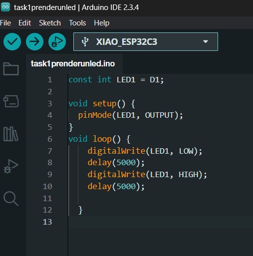
Digital signal: I quickly programmed the LED to turn on every 5 seconds. This let me identify the value when the LED lights up and then see how the value changes to 0 when it turns off.
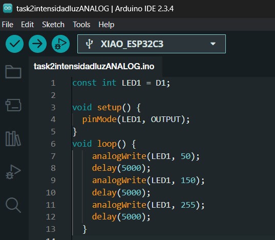
Pulse Width Modulation for analog output by switching the digital signal on and off at a high frequency.In the video you can see how the voltage is transformed from the lowest 50 that I programmed, until reaching 261, being programmed as maximum 250. As the light increases its intensity.
INDIVIDUAL ASSIGNMENT
before s t a r t i n g ‼️ ---------------->
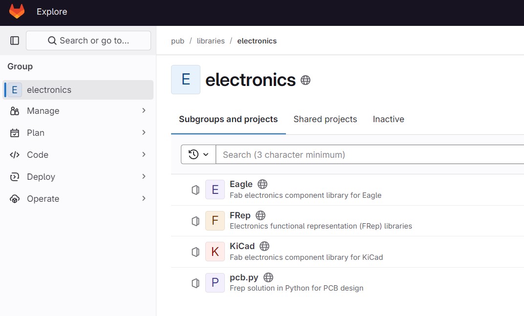
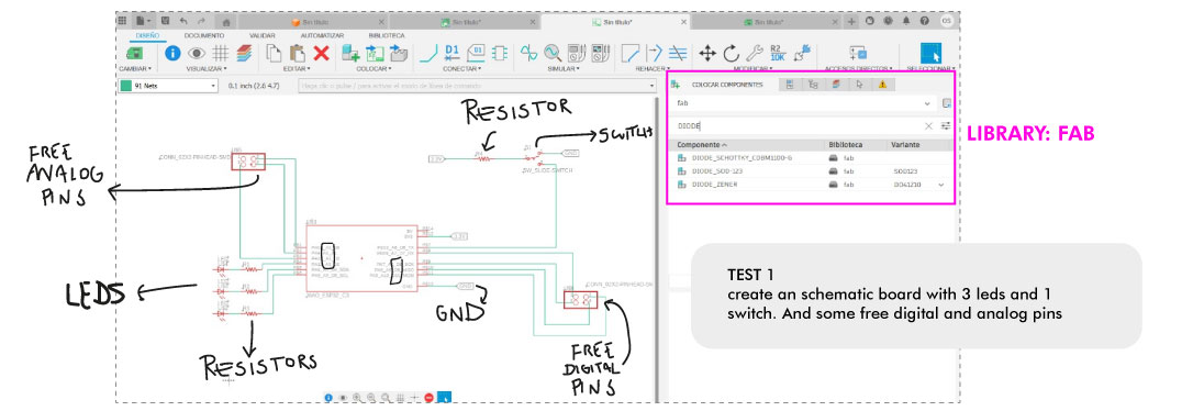
First, there is a library from the fab with all the components each lab has in this link: https://gitlab.fabcloud.org/pub/libraries/electronics so we can be sure to add components we have.
E D A t o o l E A G L E i n F U S I O N
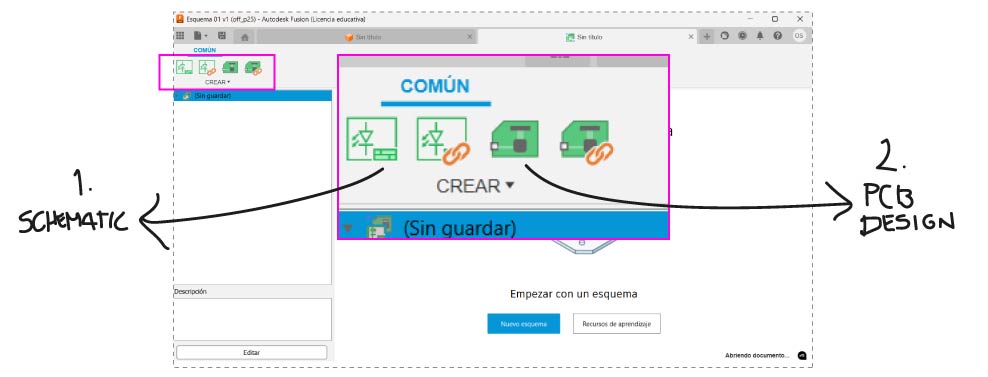
I first tried to Eagle in Fusion. To start designing a development board, first you have to make an schematic diagram to be sure about all the components an its relation in the board. Then you design the PCB (Printed Circuit Board). That its the design itself of pathway for the circuit. This is the first window when opening Fusion and NEW > Electronics.
start options
Library
Then, before starting designning we have to import the library of the components we have. There is a fab library I download from https://gitlab.fabcloud.org/pub/libraries/electronics/eagle.
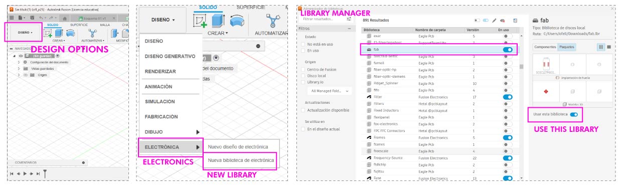
Import the library
Schematic circuit
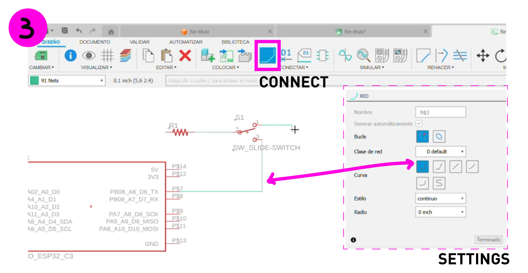
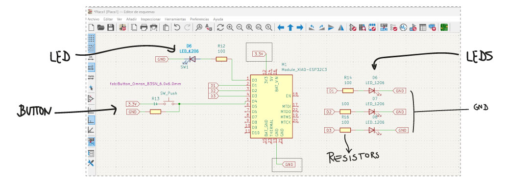
I first tried with the same components I did in the Embedded programming week: with two leds. I stablished like a shortcut to the GND so I don't have to repeat all and looks more organized for when I would have to connect more. Also both leds are connected to a 1K ohm resistor.
p r o c e s s
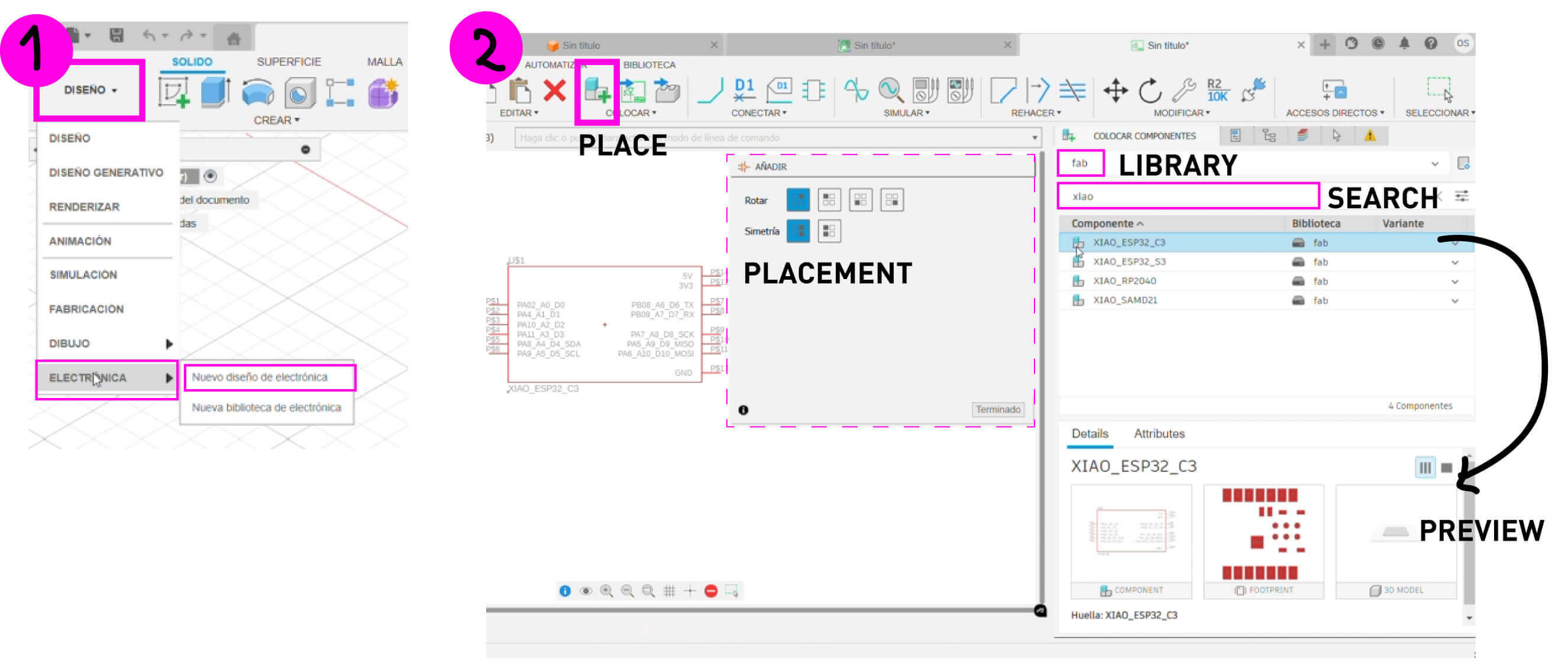
place components
connect components
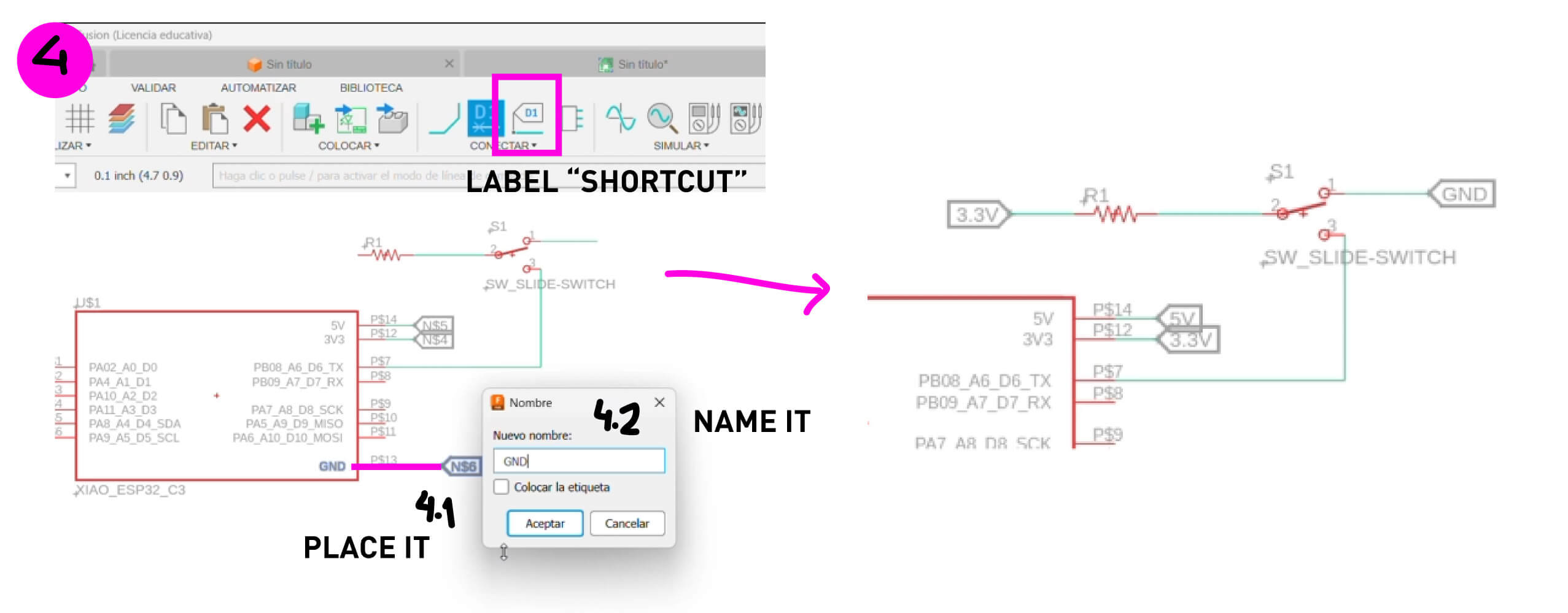
name and connect components
TEST 1: Fusion Eagle
Once the instructors showed how to use the interfaz, I started by creating the schematic board for some leds and a button or switch.
R E S U L T S :
schematic design
P C B design
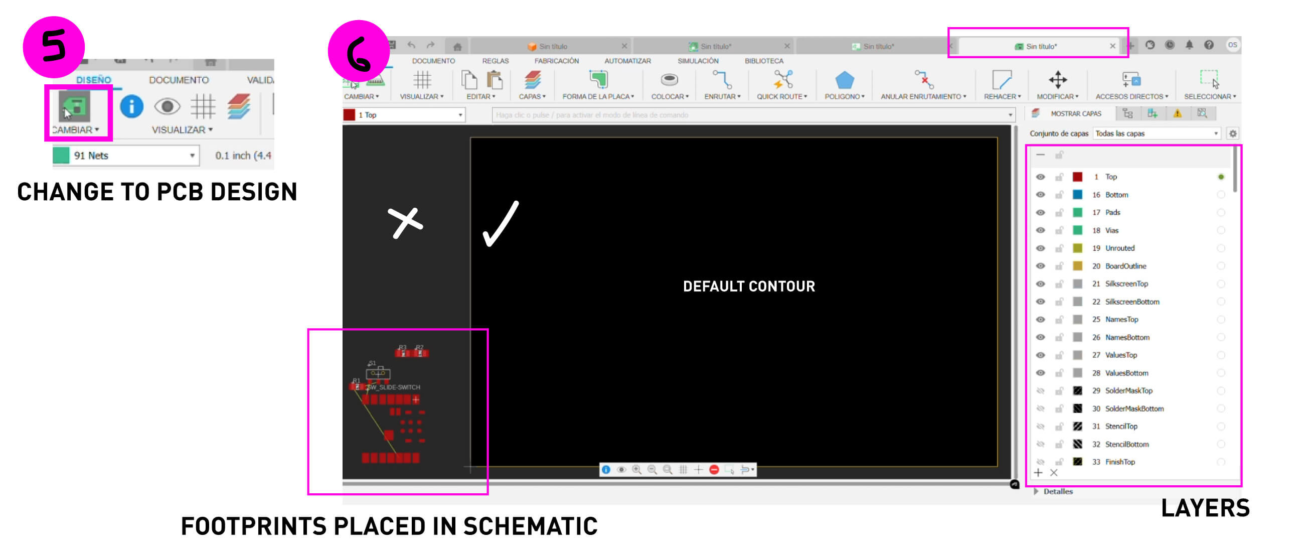
Then I changed the sketching mode to PCB where you make the real connections between the components. It must be the most efficient circuit as possible with no intersections at all.
p r o c e s s
pcb design layout
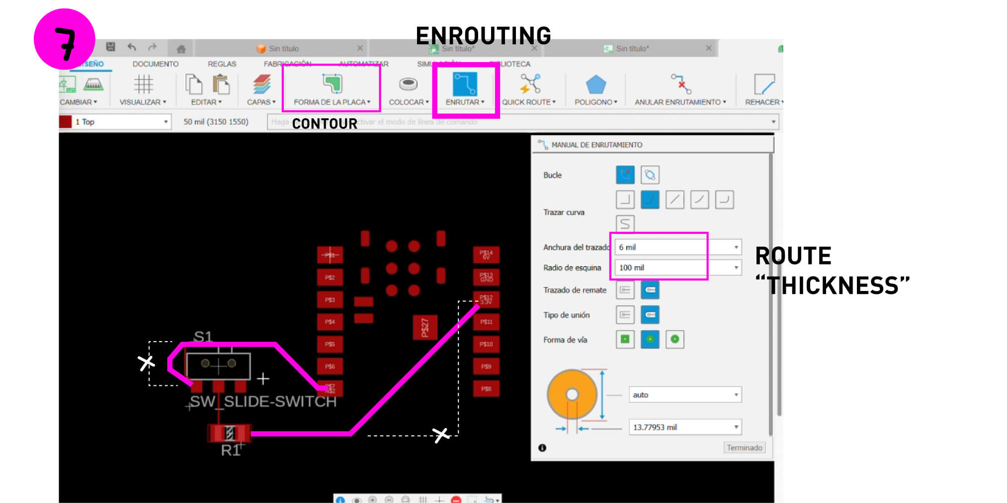
enrouting
contour
pcb circuit pathway design
P C B 3D design
I imported the fab library to Eagle from the git repo https://gitlab.fabcloud.org/pub/libraries/electronics , however it does not have the 3d components file. I explored the files and the Kicad library did had the 3d components so I also tried this workflow in order to visualize the 3d components the correct way.
E D A t o o l K I C A D
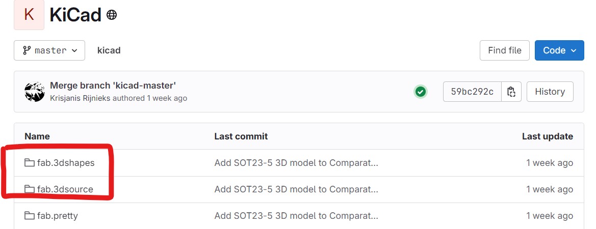
I download Kicad from https://www.kicad.org/ and first imported the library for the footprint components from the lab and also from the 3d shapes. I followed this repo from Pedro Candeias 2023 to understand how to install it, since I first did it my own and could not see the 3d shapes because they are in another folder.
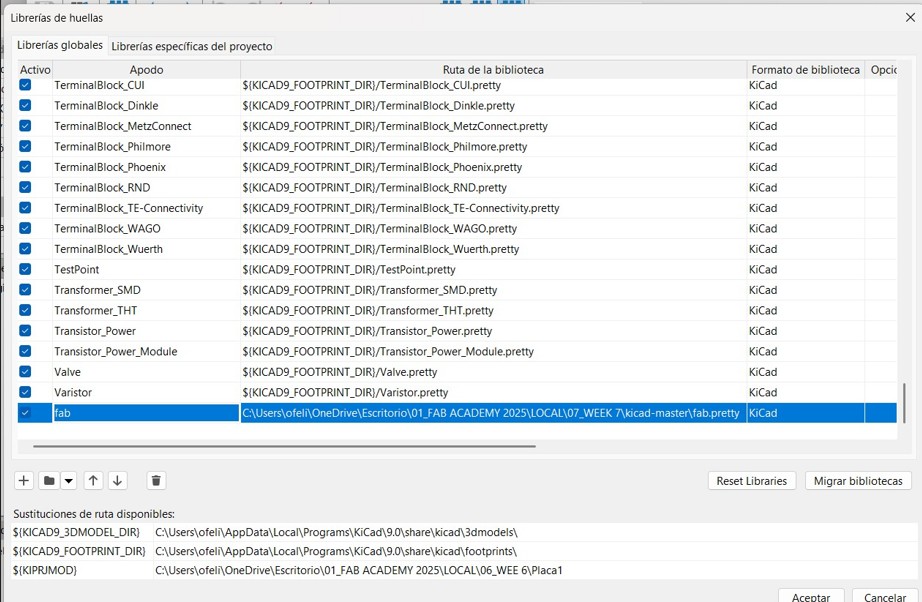
- It is important to save the folder in the general Kicad folder ~/kicad/libraries.
- First import the symbols in "Preferences / Manage Symbol Libraries" and add fab.kicad_sym as a symbol library.
- Then import the footprints "Preferences / Manage Footprint Libraries" and add fab.pretty as footprint library.
- To see the 3D components use the 3D shapes file in "Preferences / Configure Paths" here add ANOTHER named FAB that points to the installation directory of the fab library, such as ~/kicad/libraries/fab or C:/kicad/libraries/fab. This will enable the custom 3D shapes to be found.
add footprint library
for the 3d components ‼️
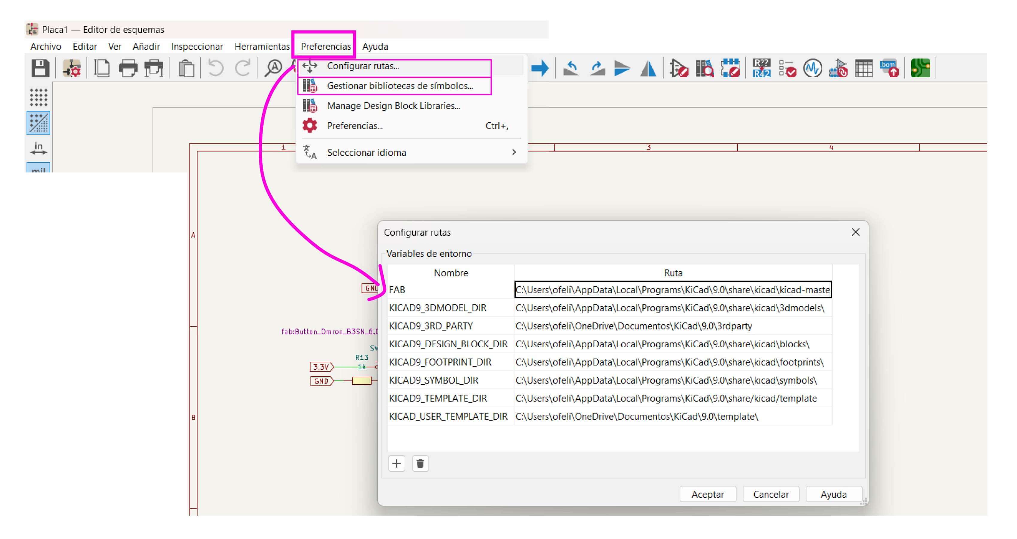
add 3d shaes file in configure paths.
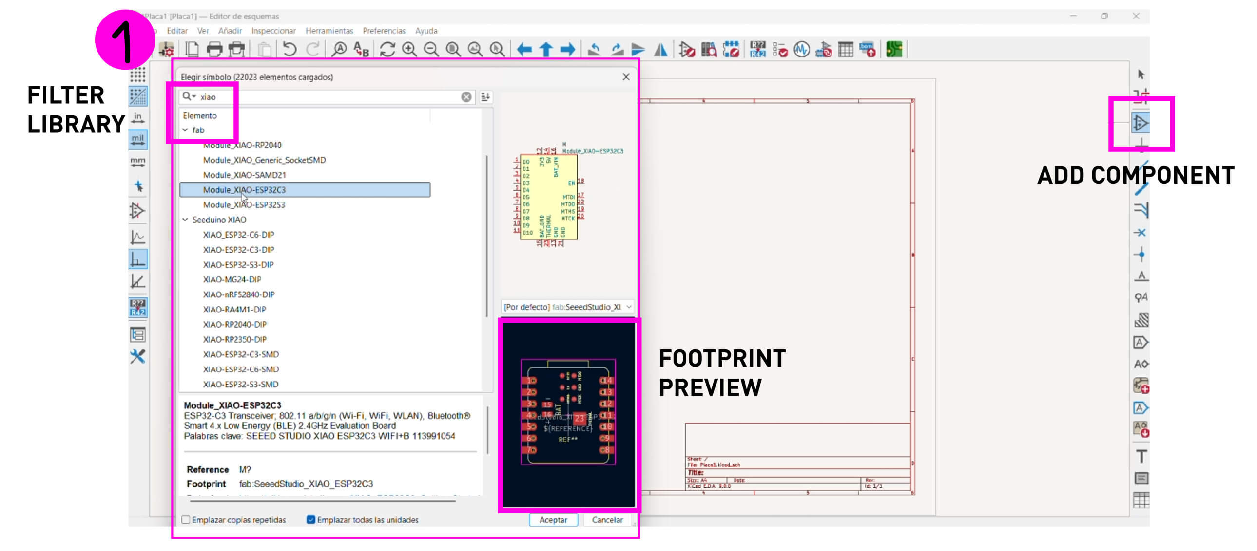
Schematic in kiCad
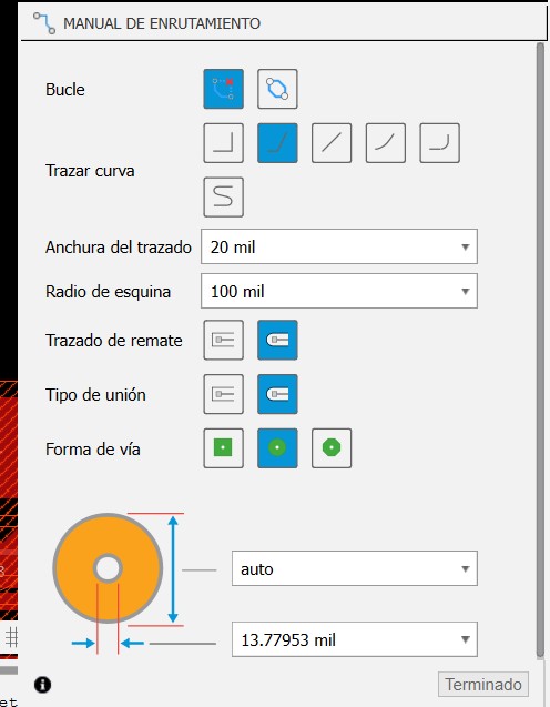
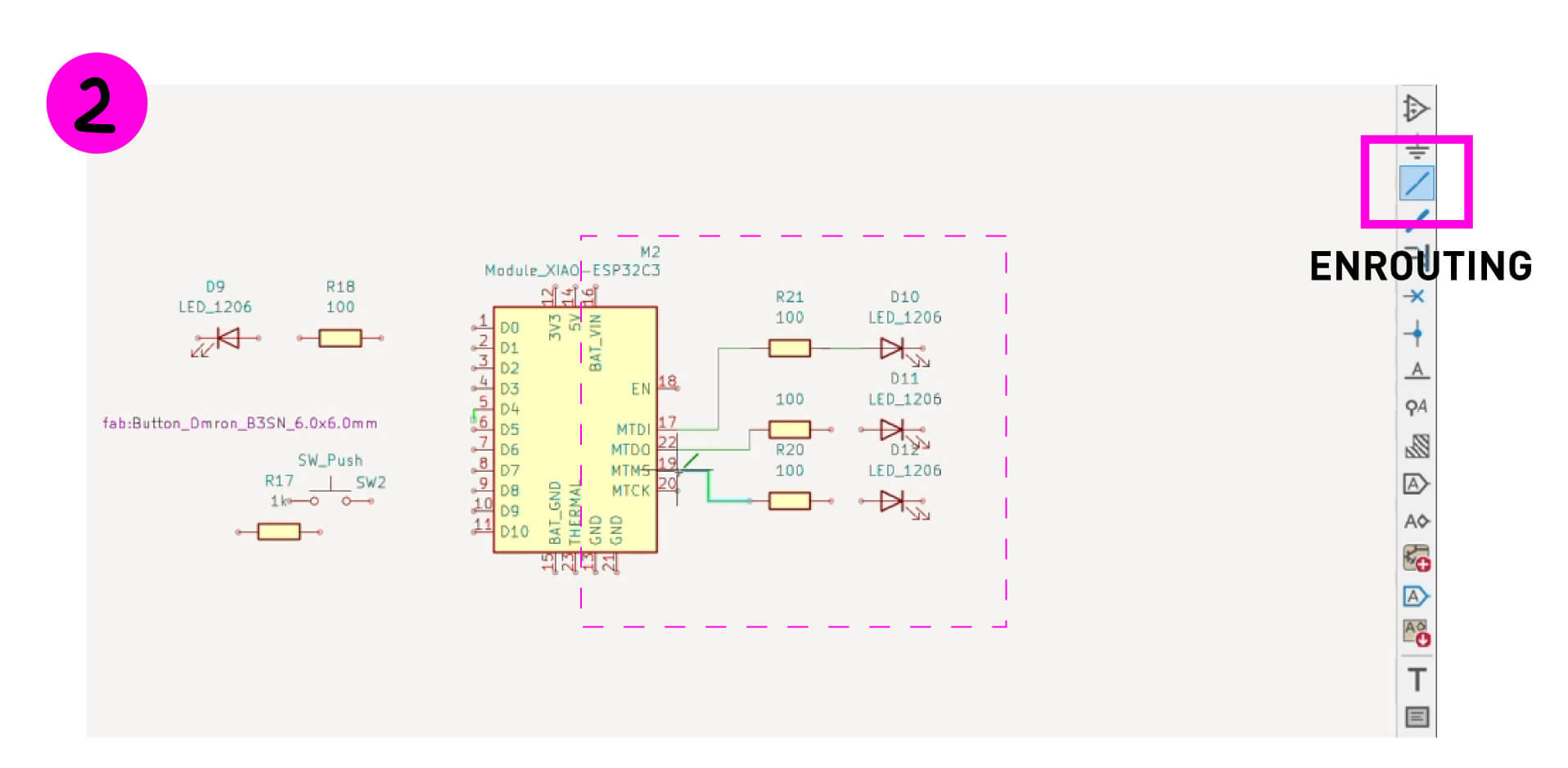
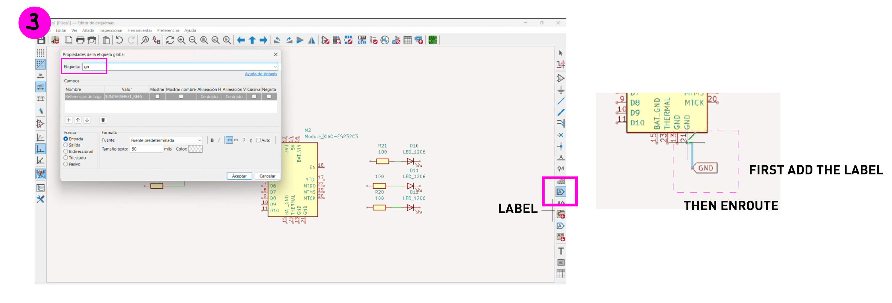
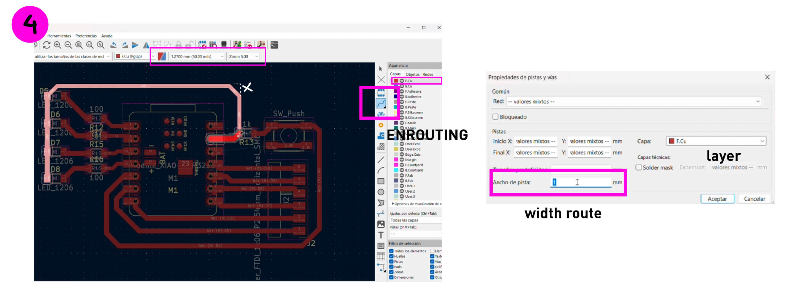
As in Fusion, I could filter the components by the fab library. For making the routes there opens a route settings window where you can change the thickness. However for the labels first you have to put and name the labels and then connect them.
p r o c e s s
pcb design layout
enrouting
contour
In this schematic design I divide the order with labels for the leds so it can be more clear to understand where they go. If not it will be too much components next to each making difficult to read.
schematic design
PCB design kiCad
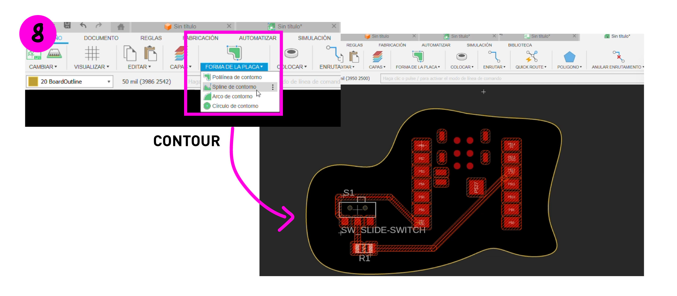
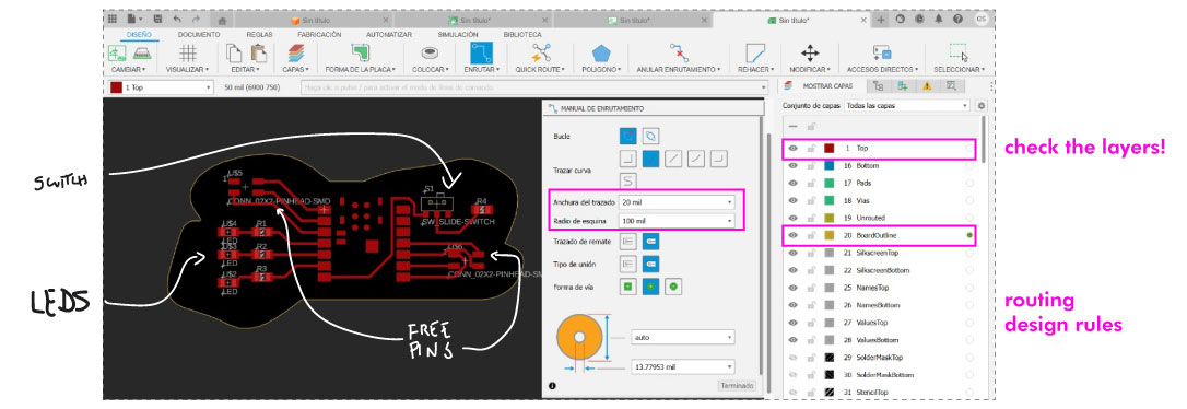
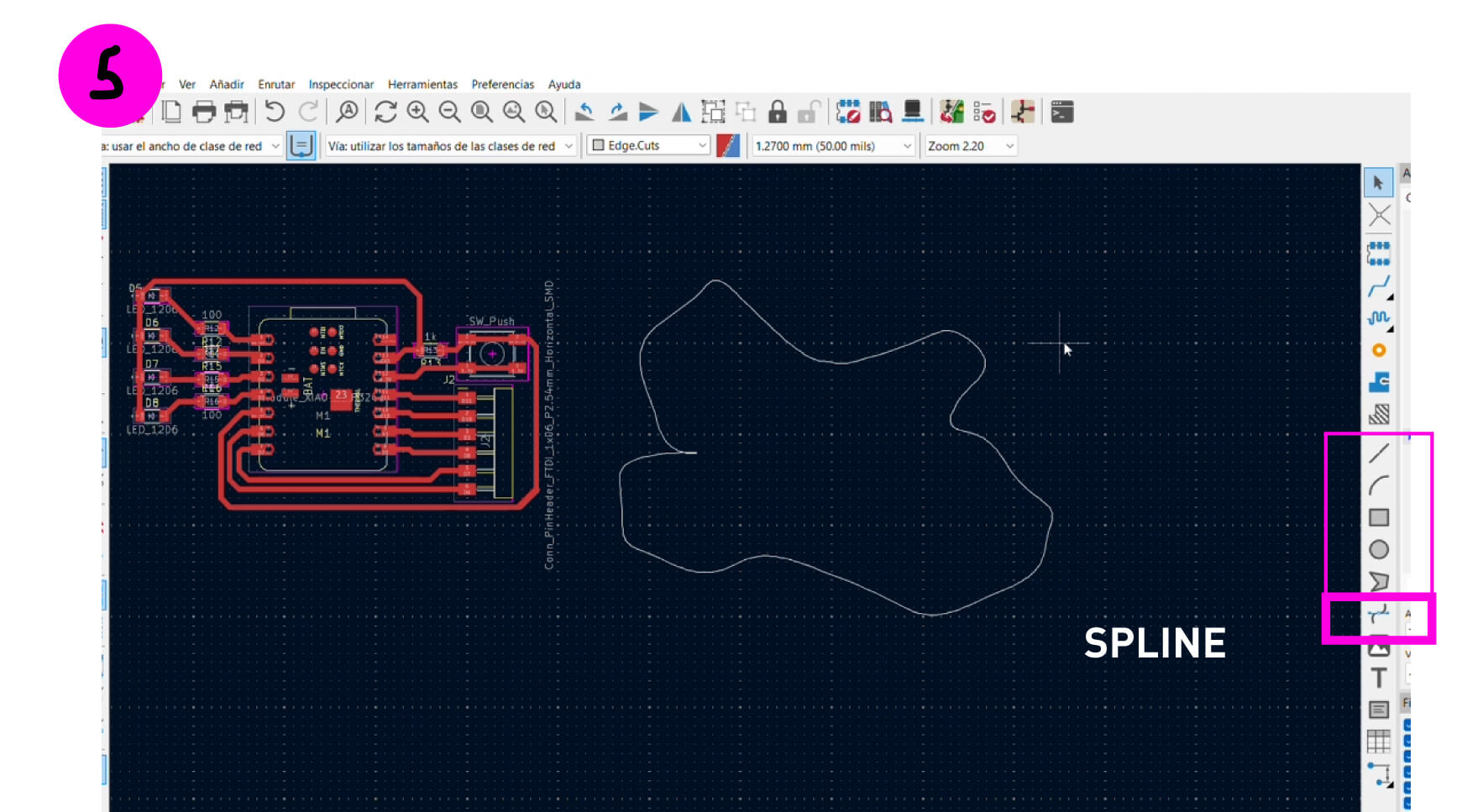
The same way you can find layers where to enroute. It will also open a settings window to check the design rules. I found it easier here to make a curve contour.
p r o c e s s
connecting
making a contour curve.
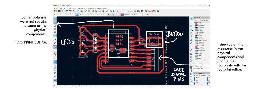
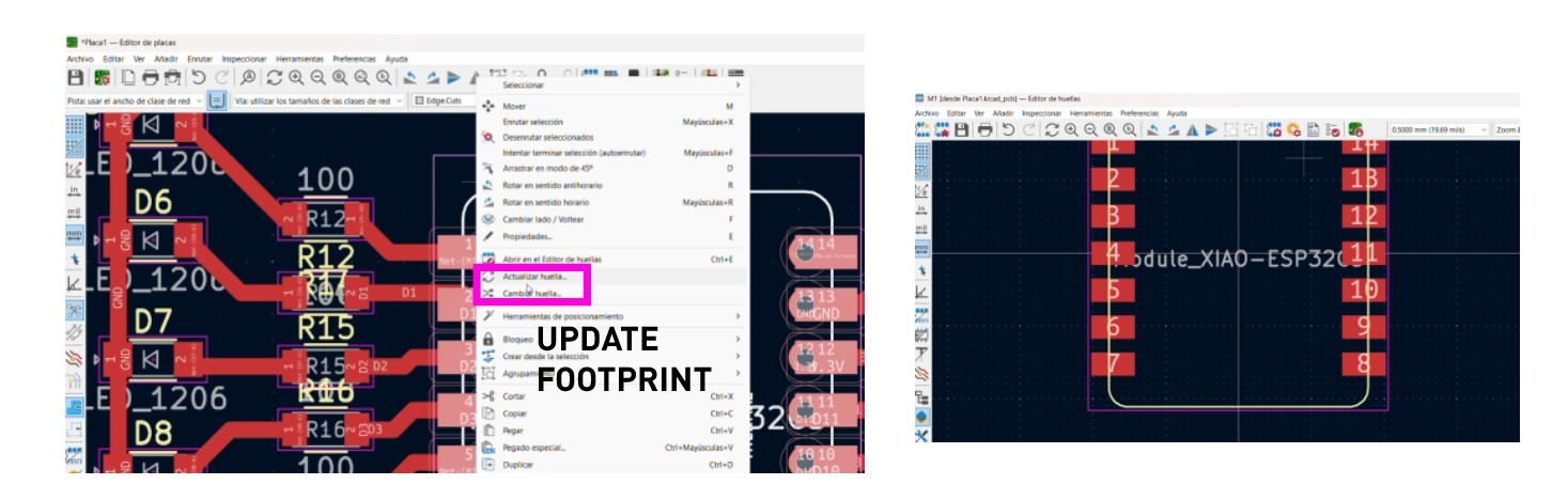
Update the footprint of the components if they are not 100% accurate. The space in this components will leave the thickness of the circuit designed.
pcb circuit pathway design
We can update the footprints of the components to check measures.
edit footprint
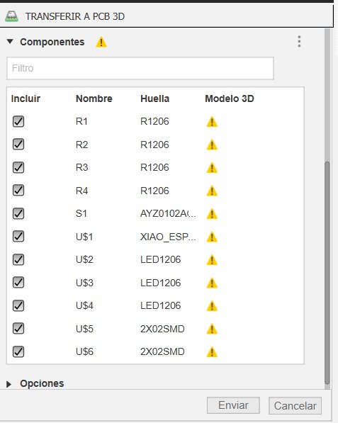
P C B 3D design
Changing to the 3d visor, in Kicad all the 3d components show. Seeing it in 3D made me realize that the try to make the contour smooth was not working fine. Then I move to SPLINE option to make de border and it show off better.
KICAd 3d VISOR
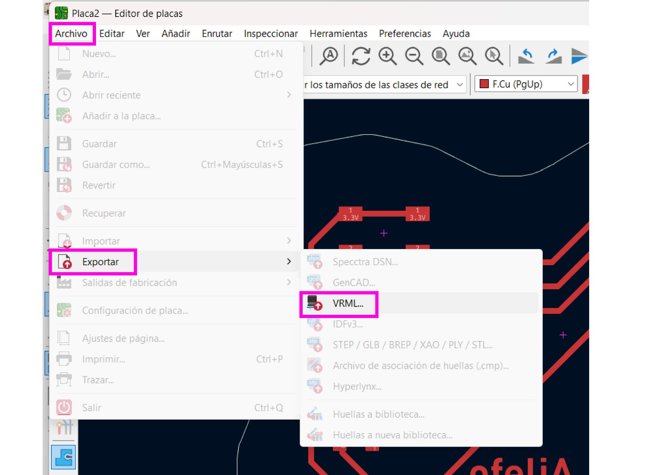
KiCad EXPORT
You can export the 3d visor preview as VRML. I opened this file in Rhinoceros and worked fine. From the layouts you can select to export just the board, thecomponents and also the engraving.
export 3d view.
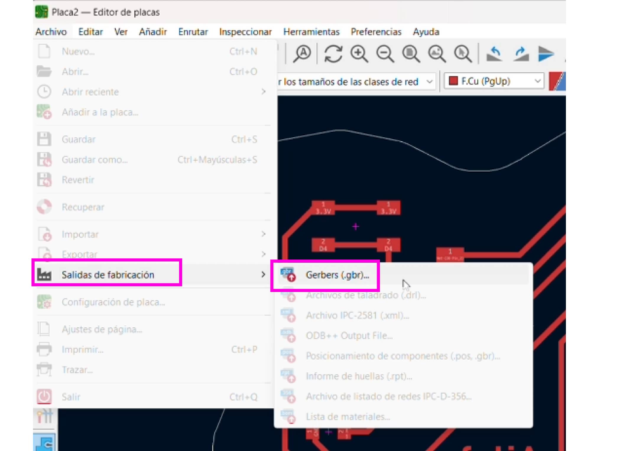
An to fabricate this I expored this in FABRICATION MODE as G E R B E R.
export in fabrication mode.
e x t r a: C A S E for the pcb board
3d printing case