Week 6
Electronics Design
My specific task for this FabAcademy week was to design a microcontroller development board. In parallel, our group project involved a thorough examination of the microcontroller's datasheet, which enabled us to contrast its development processes and performance with those of other architectures. This thorough approach improved my knowledge of embedded programming and gave me important new perspectives on the wide range of microcontroller designs and their uses.
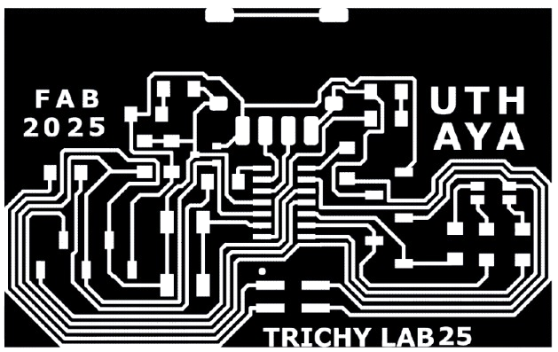
My heroshot for this week:
Basics of electronics:
Electronics involves the study and application of devices and circuits that control the flow of electrons to perform tasks like data processing, signal amplification, and information transmission. Key concepts include voltage, current, resistance, inductance, and capacitance, which are essential for understanding how electronic devices work.
Key Concepts in Electronics:
Basic Electronic Components:
Problems, Challenges and Solutions
-
Problem 1: Understanding the Microcontroller Datasheet
- Challenge: The datasheet was very detailed and technical, making it hard to quickly find the important parts.
- Solution: Breaking it into smaller sections power, pin configuration, communication protocols and studying them one by one made it much easier to follow and apply.
-
Problem 2: Designing the Development Board in the EDA Tool
- Challenge: Placing components correctly and making proper connections without errors was confusing at first.
- Solution: Reference designs were checked, pin mappings were carefully verified, and the design rule check (DRC) tool helped fix mistakes along the way.
-
Problem 3: Soldering Small Components
- Challenge: SMD components were tiny and difficult to handle during soldering.
- Solution: Using tweezers, flux, and a magnifying lens made the work easier. Practicing on scrap boards also built up confidence.
-
Problem 4: Testing the Board
- Challenge: The board didn’t work on the first try, and finding the exact error was tricky.
- Solution: Continuity was checked with a multimeter, the power supply was verified, and solder bridges were inspected. After debugging, the board worked properly.
-
Problem 5: Time Management
- Challenge: Managing both group work and individual tasks within the deadline was stressful.
- Solution: A simple timeline with daily task division helped complete everything on time without missing important details.
Group Assignment:
- Use the test equipment in your lab to observe the operation of a microcontroller circuit board (in minimum, check operating voltage on the board with multimeter or voltmeter and use oscilloscope to check noise of operating voltage and interpret a data signal).
- Redraw one of the echo hello-world boards or something equivalent, add (at least) a button and LED (with current-limiting resistor) or equivalent input and output, check the design rules, make it, test it.
- Linked to the group assignment page. Click to open our Group Assignment
Outcomes
Use the test equipment in your lab to observe the operation of a microcontroller circuit board
Documenting work on the group work page and reflect what you learned on your individual page
Individual assignments:
Use an EDA tool to design a development board to interact and communicate with an embedded microcontroller, produce it, and test it
reference links


Individual Assigment:
Development Board:
My plan for this week is to design, mill, test a development board.
Design:
I'll be designing a development board using SAMD11.
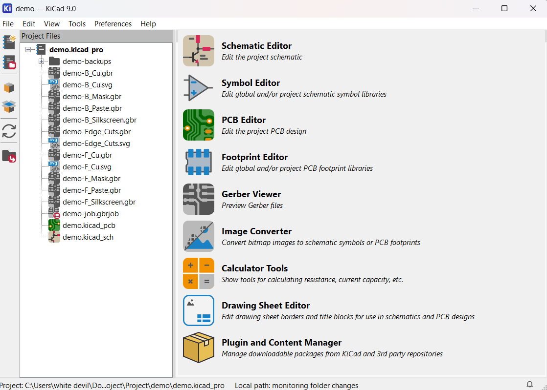
KiCad:
KiCad is an open-source EDA software suite for designing PCBs and schematics. The typical workflow in KiCad involves two primary tasks: drawing a schematic and laying out a circuit board. A KiCad project encompasses various files within a folder, including a project file, schematic, board layout, and potentially other associated files like symbol and footprint libraries, simulation data, and purchasing information.
The process begins with creating a schematic, where components are selected from libraries and connected using wires to represent electrical connections. After completing the schematic, an Electrical Rules Check (ERC) is performed to ensure the design's integrity. It's common for schematics to undergo revisions even after the board layout has begun, necessitating updates and iterations to maintain consistency.
Once the schematic is finalized and passes the ERC, the design is transferred to the board editor. Here, the netlist generated from the schematic is imported, and footprints for components are automatically placed on the board. Designers then arrange these components, taking into account factors like size, placement, and signal routing. Traces are drawn to establish electrical connections between components, adhering to design rules and constraints.
After laying out the board, a Design Rules Check (DRC) is performed to ensure compliance with manufacturing specifications. Any errors or warnings identified during this check are addressed to ensure manufacturability. The board layout undergoes thorough review to confirm alignment with design requirements before saving the final layout.
Once the board layout is complete and passes the DRC, fabrication outputs are generated.
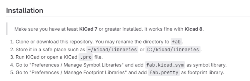
To add components while designing there are a lot of libraries but for Fab Academy, there is a seperate library with all components. This avoids confusion since there are multiple libraries with same components.
Next step to follow these installation steps mentioned in the repository for correct access to the library while designing. So i followed those steps.
SAMD11:
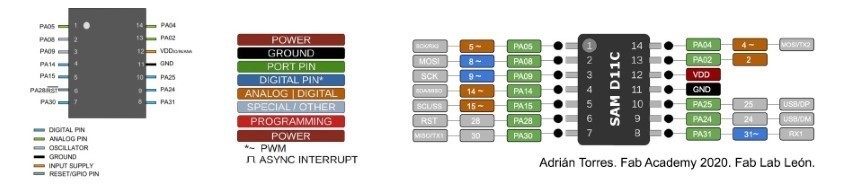
Microchip Technology created the SAM D11 microcontroller. It is a member of the ARM Cortex-M0+ based SAM D family of microcontrollers. Because of their low power consumption, SAM D11 microcontrollers are appropriate for situations where energy efficiency is crucial. They are frequently utilized in consumer electronics, IoT devices, embedded systems, and other applications that need for moderate computing capability and low power consumption. SAM D11 microcontrollers are adaptable for a variety of applications since they often come with a variety of peripherals, including ADCs, UARTs, SPI, I2C, timers, and GPIOs.
This SAMD11 microcontroller is what I'm utilizing for my development board. In order to comprehend the microcontroller and incorporate it into my design appropriately, I utilized this pin-out diagram.
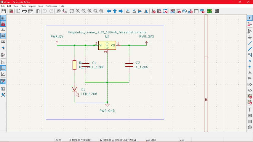
Regulator circuit:
SAMD11 runs on 3.3V but the laptop output voltage is 5 V. To regulate the voltage, I referred this design so my board would not damaged.

Here is the regulator circuit
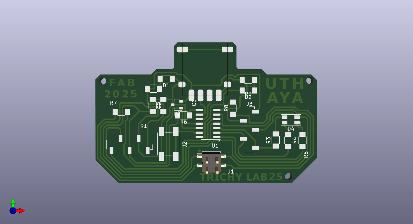
Schematic Design:
Here is the design with all components:
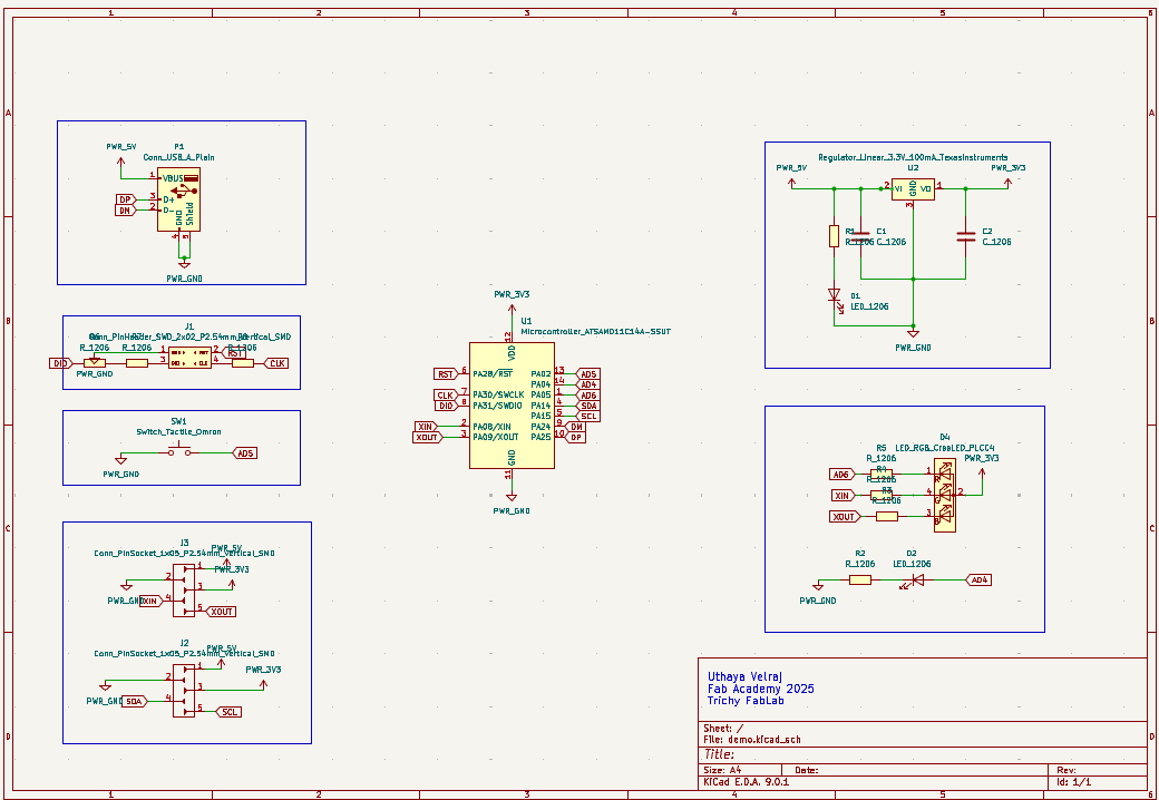
I created a voltage regulator circuit to provide the microcontroller with 3.3V in order to comprehend the concept. To make soldering easier, I'm using 1x04 header pins rather than 2x05 header pins. In reality, the USB_A plain is a stand-in for the USB C type breakout board, which we soldered during the electronics production week. I've added two pin sockets, an LED, and a button. I have connected the chip's SDA and SCL, as well as 5V, 3.3V, and GND, to one socket designated for I2C. I connected XIN, XOUT, the last digital pin, GND, and 5V to the socket after that. Every pin on the board has been labeled by me.
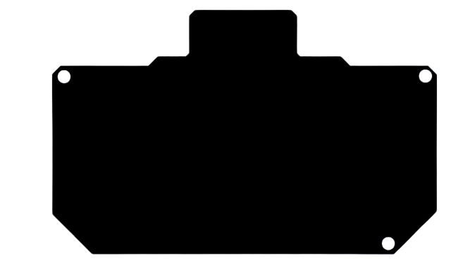
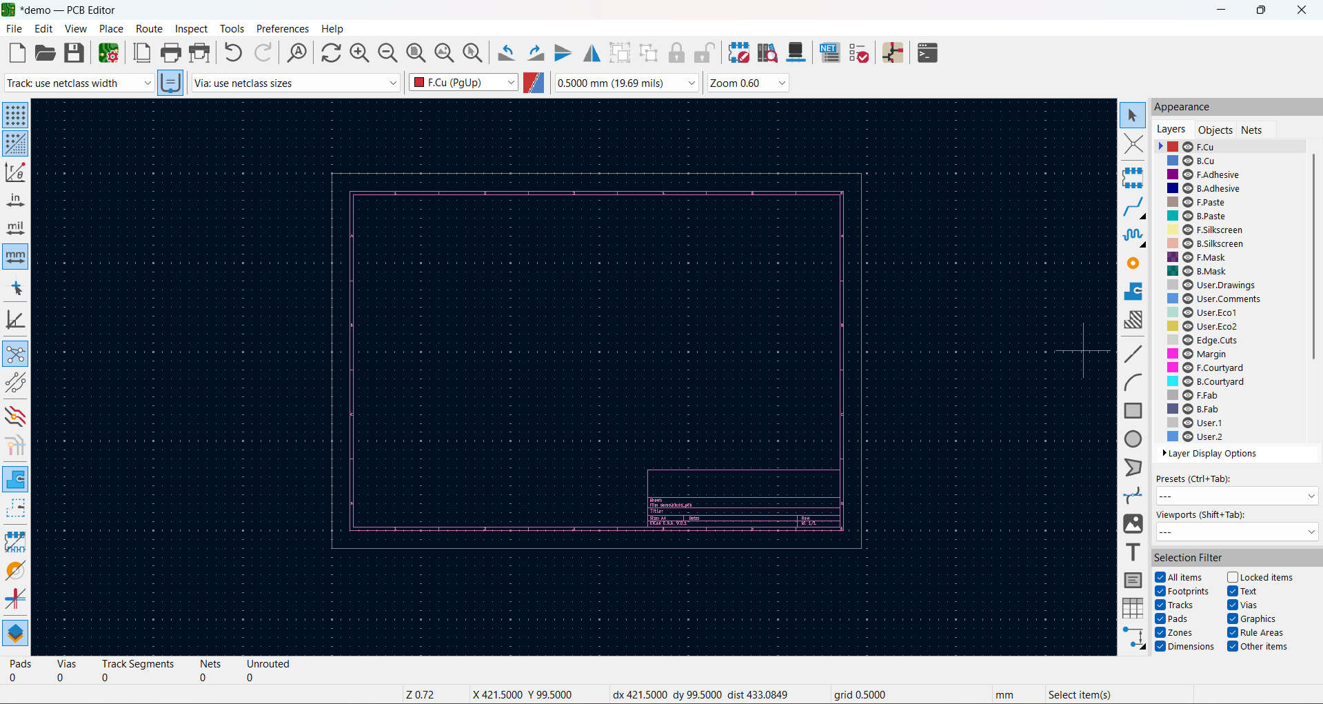
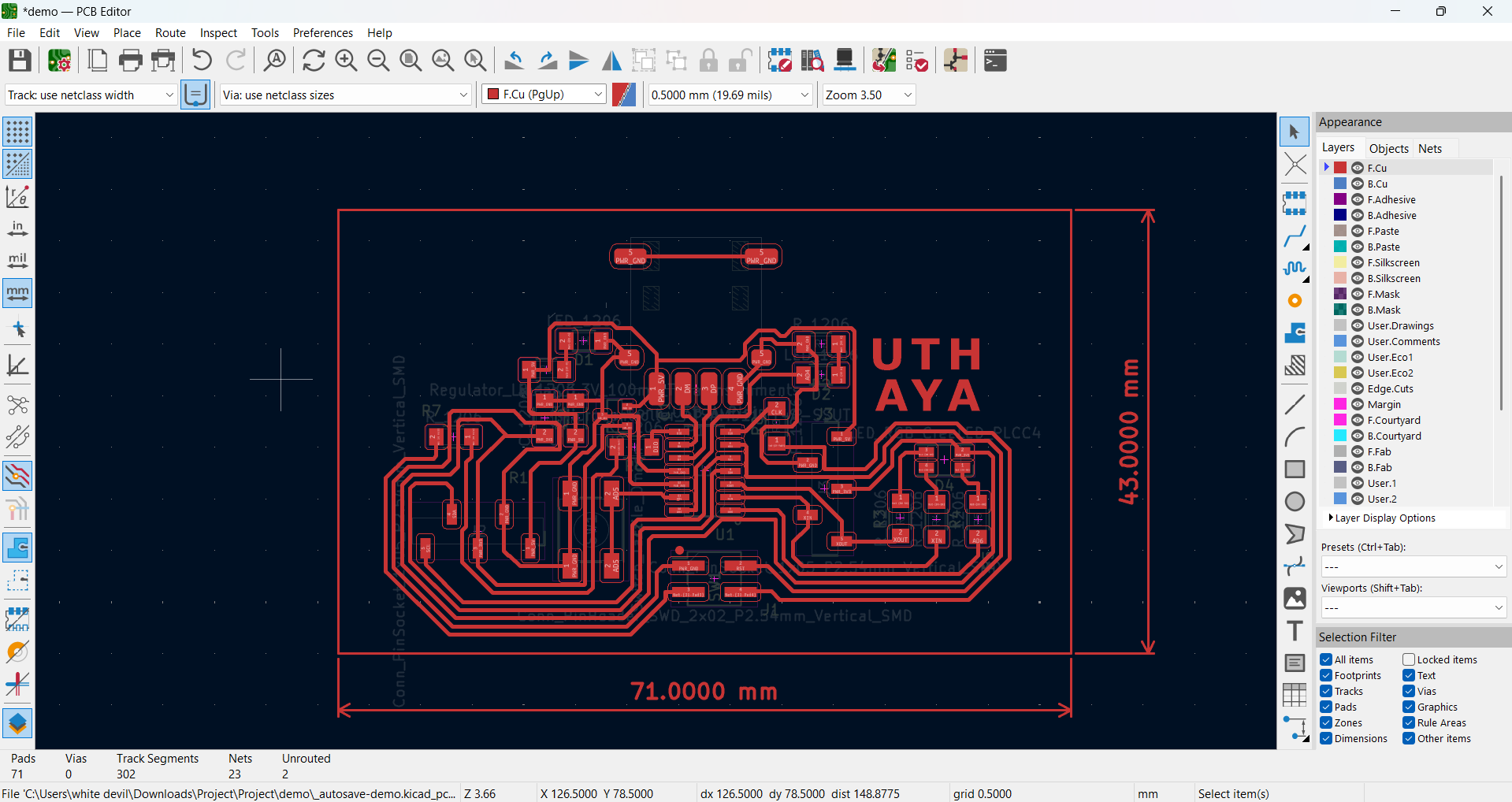
PCB Design:
- Schematic design is done and next step is the design of PCB layout of the circuit. So I opened PCB editor.
- Then import the design onto the editor.
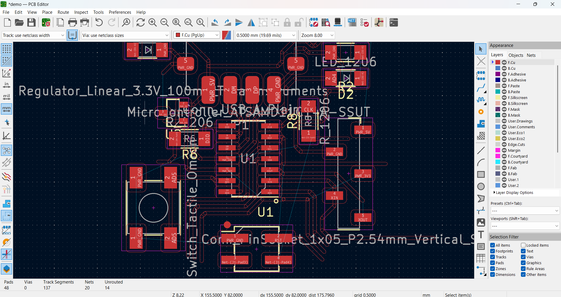
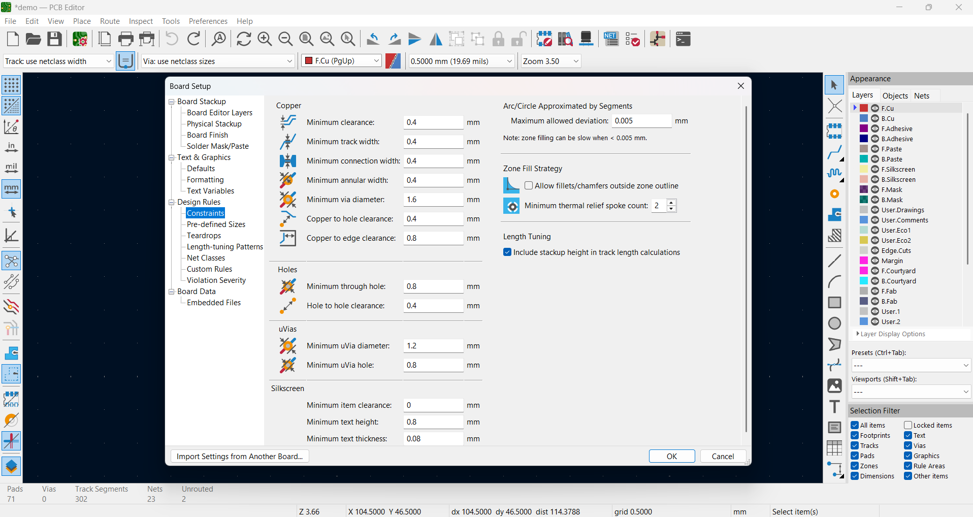
- Next step is set the constraints of the route tracks optimised for the milling bit.
- Here's the result after almost 10 hours of routing. Had to add three jumpers.
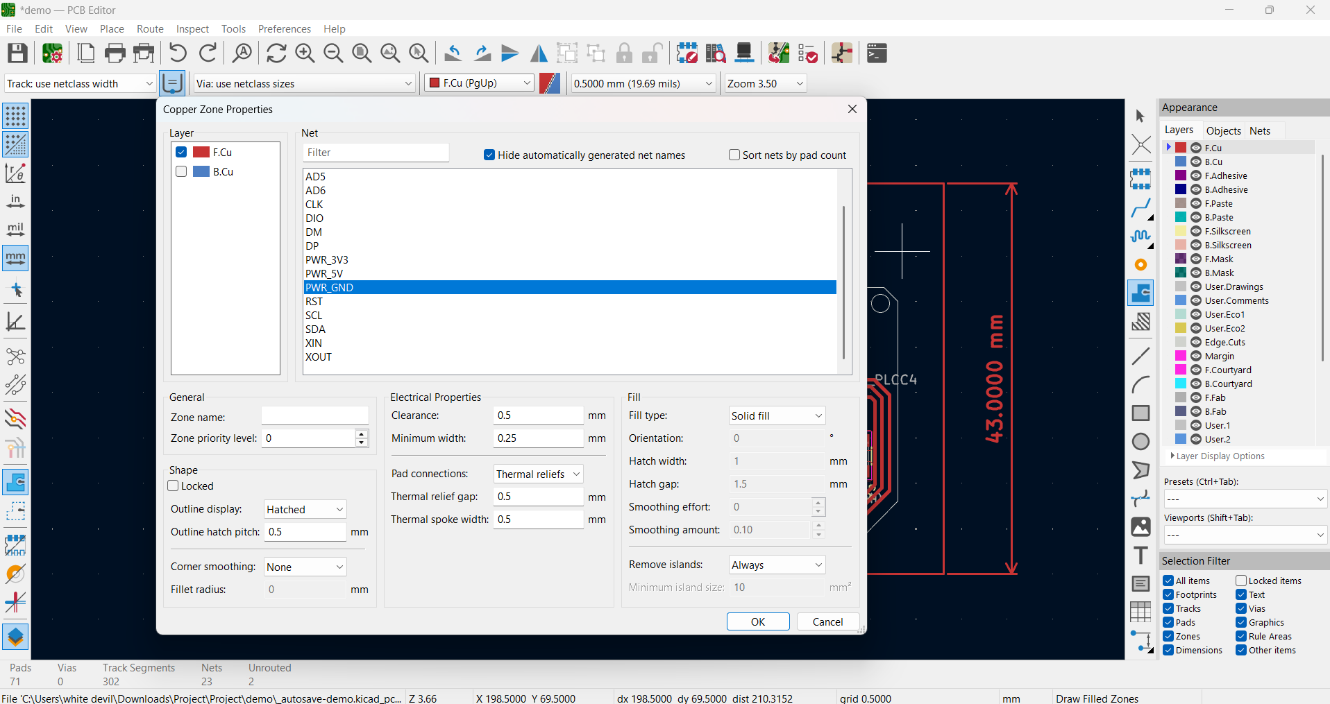
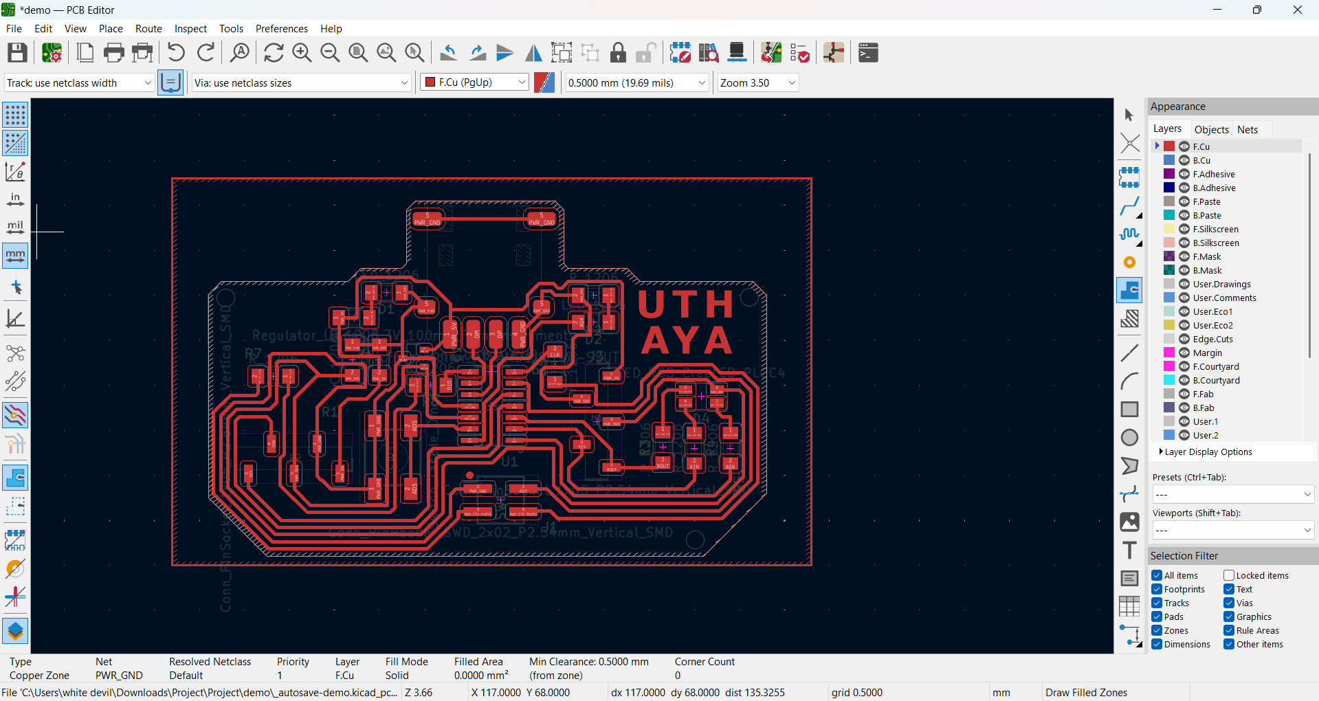
- Next I poured copper onto the top layer. So I selected the top layer and chose add filled zones. I chose net as PWR_GND.
- Here's the result:
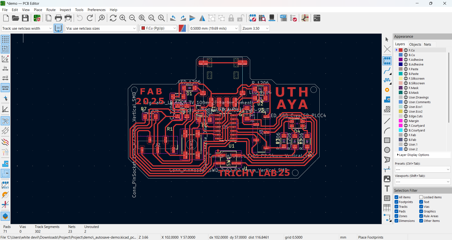
- Few changes were made to the design
- 3D view of the design
Exporting the files:
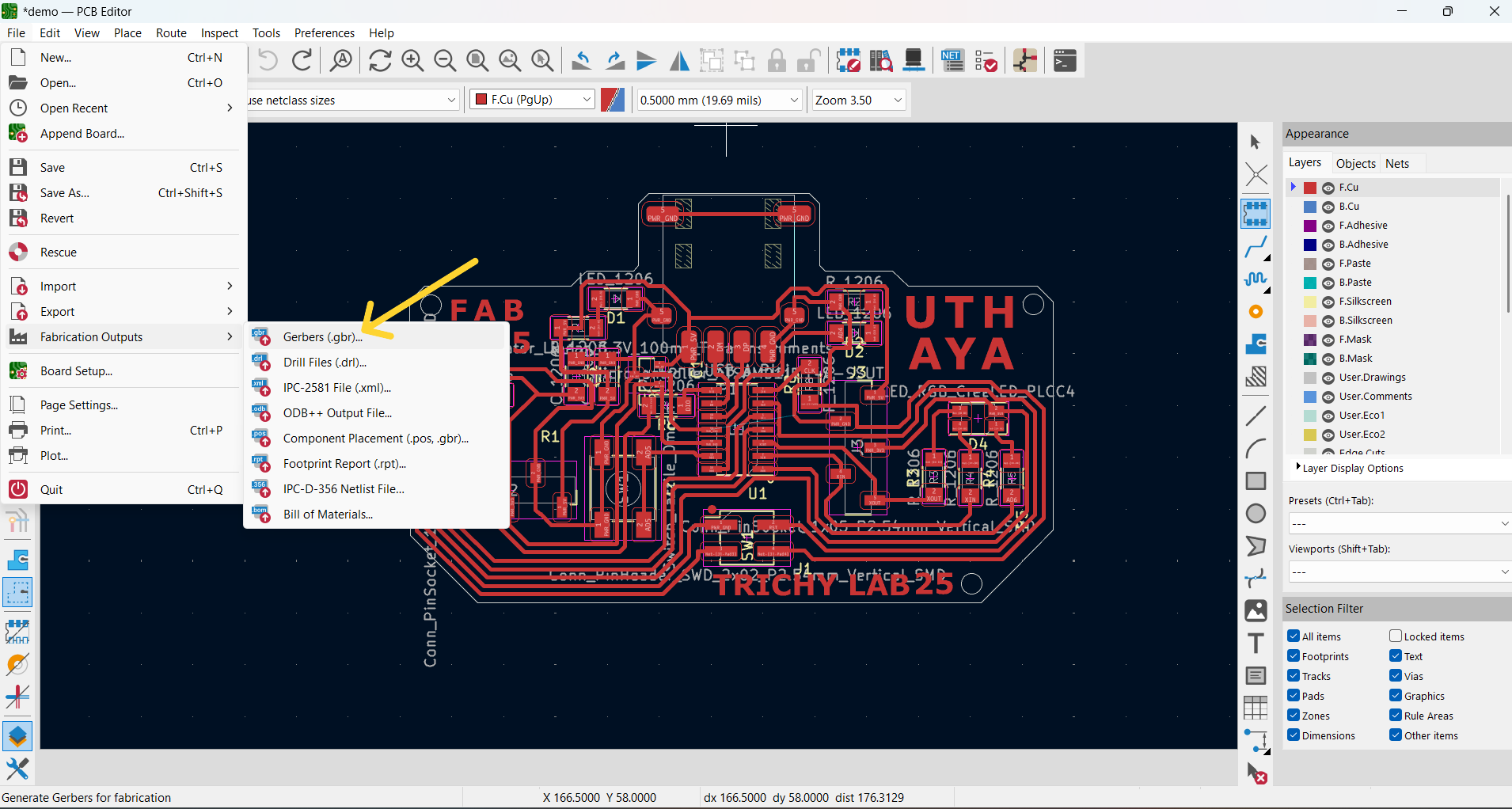
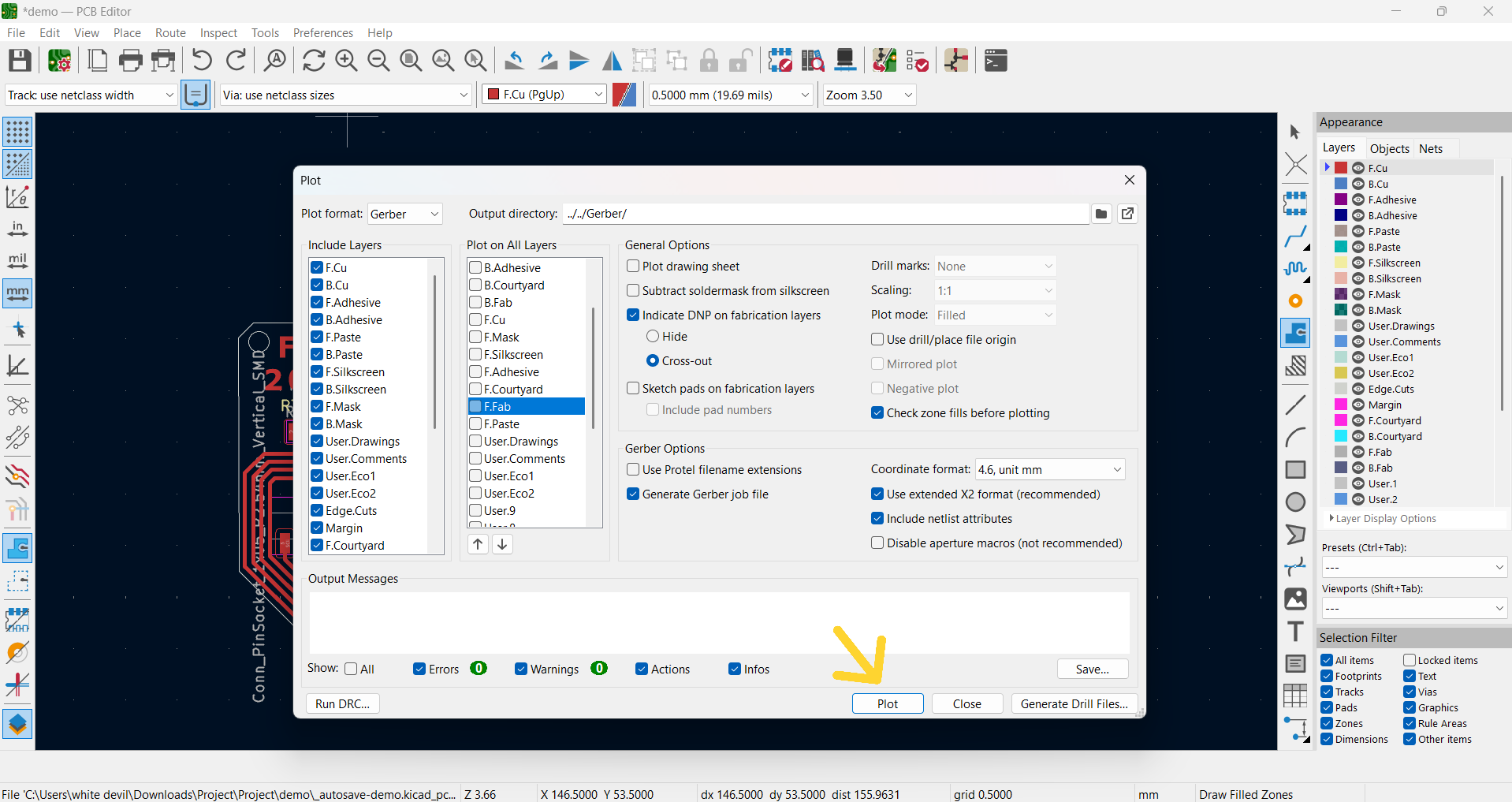
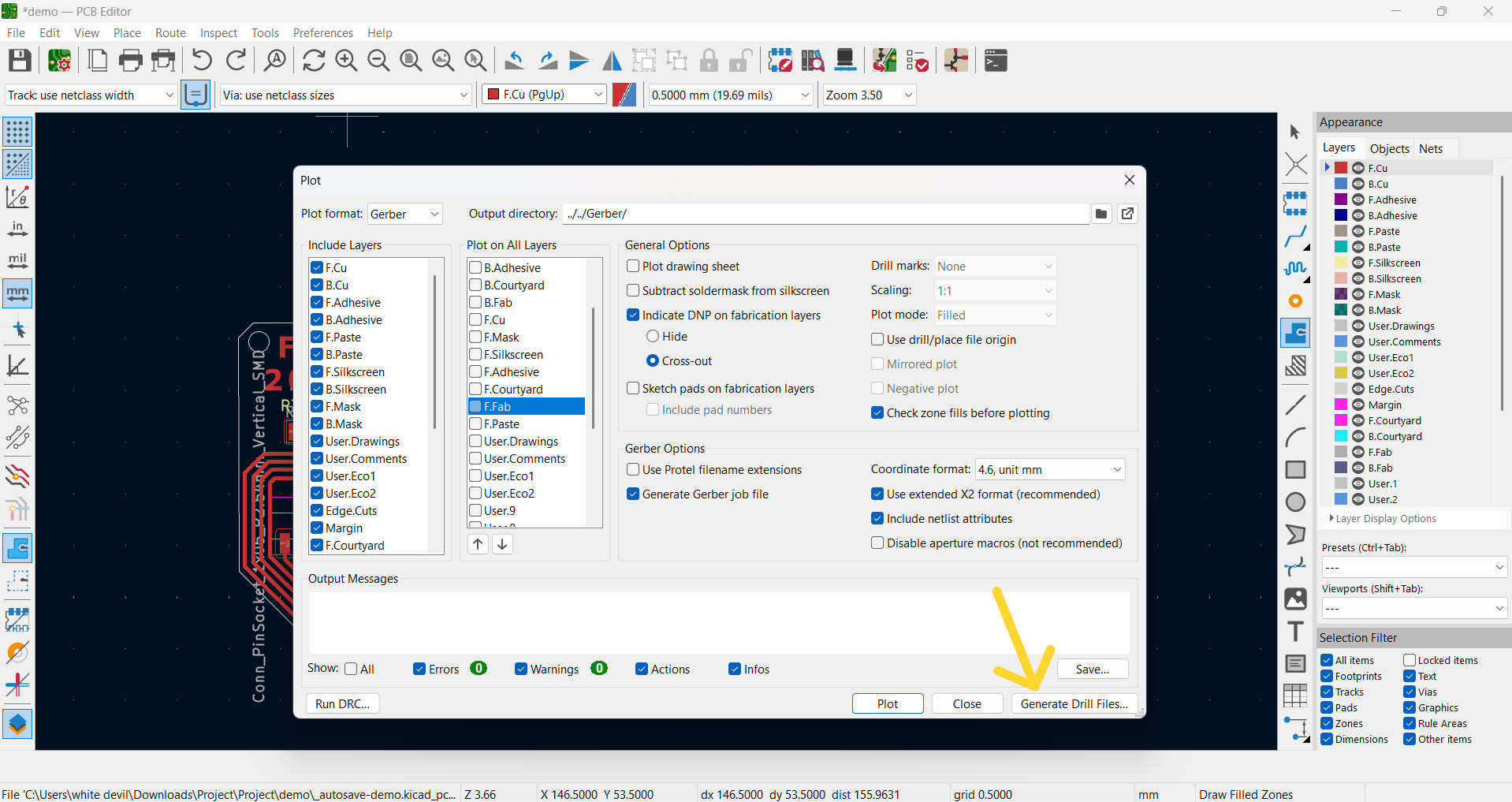
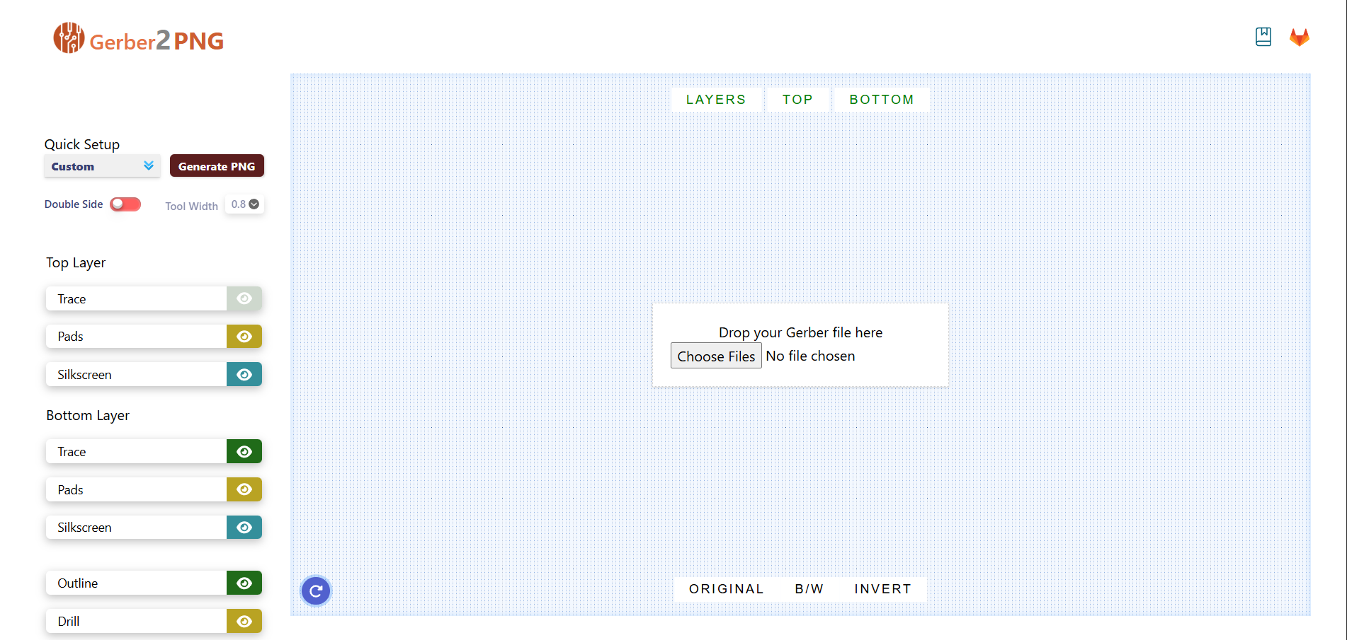
Gerber to PNG:
Next step is to convert the exported Gerber file into PNG for milling. I used Kerala FabLabs special website for this conversion. Visit this website.
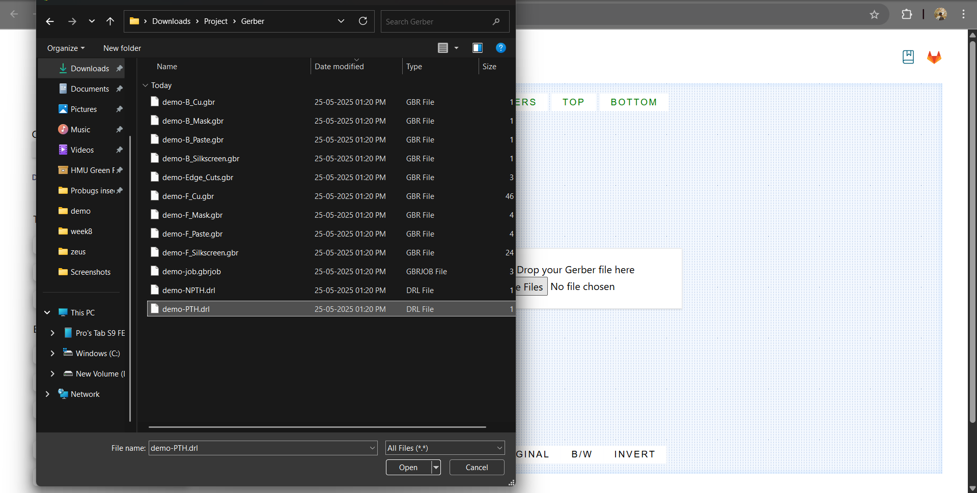
- So first, I uploaded all those files into this website.
- The files have been uploaded.
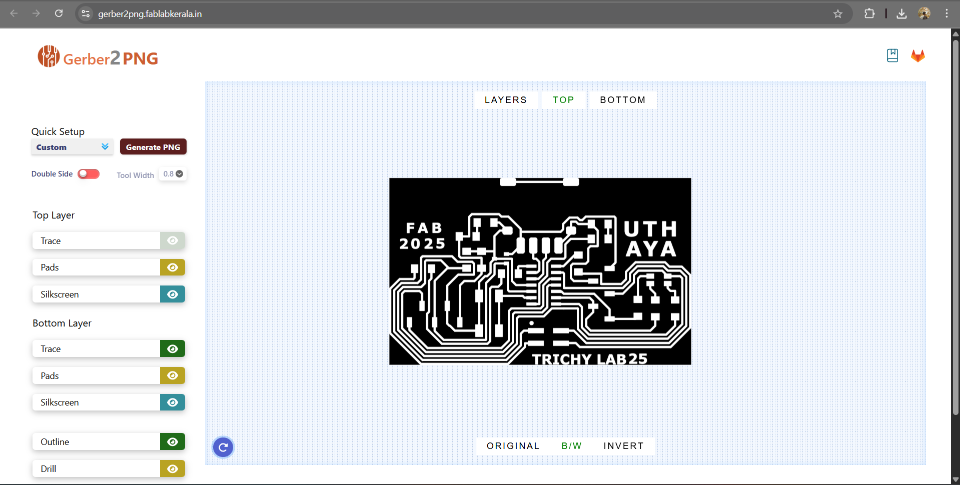
Here are the files: