Group Assignment
Group Assignment Summary
As part of the group assignment, we characterized the PCB production process available in our lab. We tested and evaluated the PCB milling workflow by preparing toolpaths, selecting suitable milling bits, and fabricating sample circuit boards. Different milling parameters such as cut depth, feed rate, and tool diameter were analyzed to understand their effect on trace quality and board accuracy. We also examined the capabilities and limitations of the PCB milling machine, verified trace isolation, and inspected the final milled boards for manufacturing quality. This exercise helped us establish reliable settings for producing accurate PCBs and provided valuable experience in digital fabrication, machine operation, and quality control during electronic production
Hero Shot
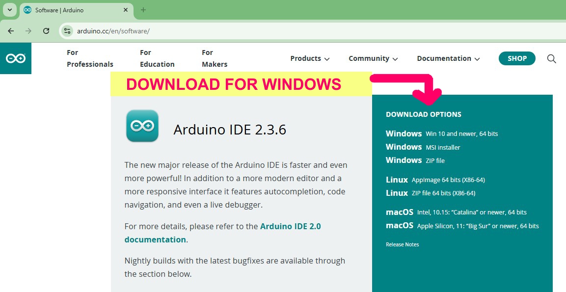
Click Here:Week-06 Electronics Design.
My Objective
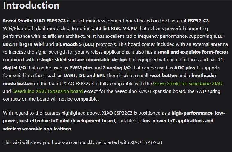
My objective is to design a simple PCB with 2 LEDs, 3 resistors, and a button switch using KiCad. I verified the circuit, generated toolpaths, milled the board, soldered components, and uploaded the code. This process was done under the Seeed Studio workflow for Week 8 Electronics Production.
Tools Required
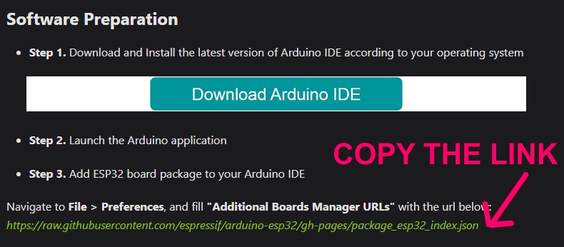
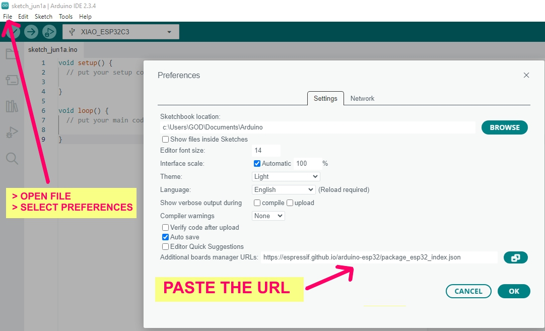
- KiCad (for schematic and PCB design)
- Mods CE for toolpath generation
- CNC milling machine Wegstr Machining
- Double-sided PCB blank
- Soldering tools
- Multimeter etc
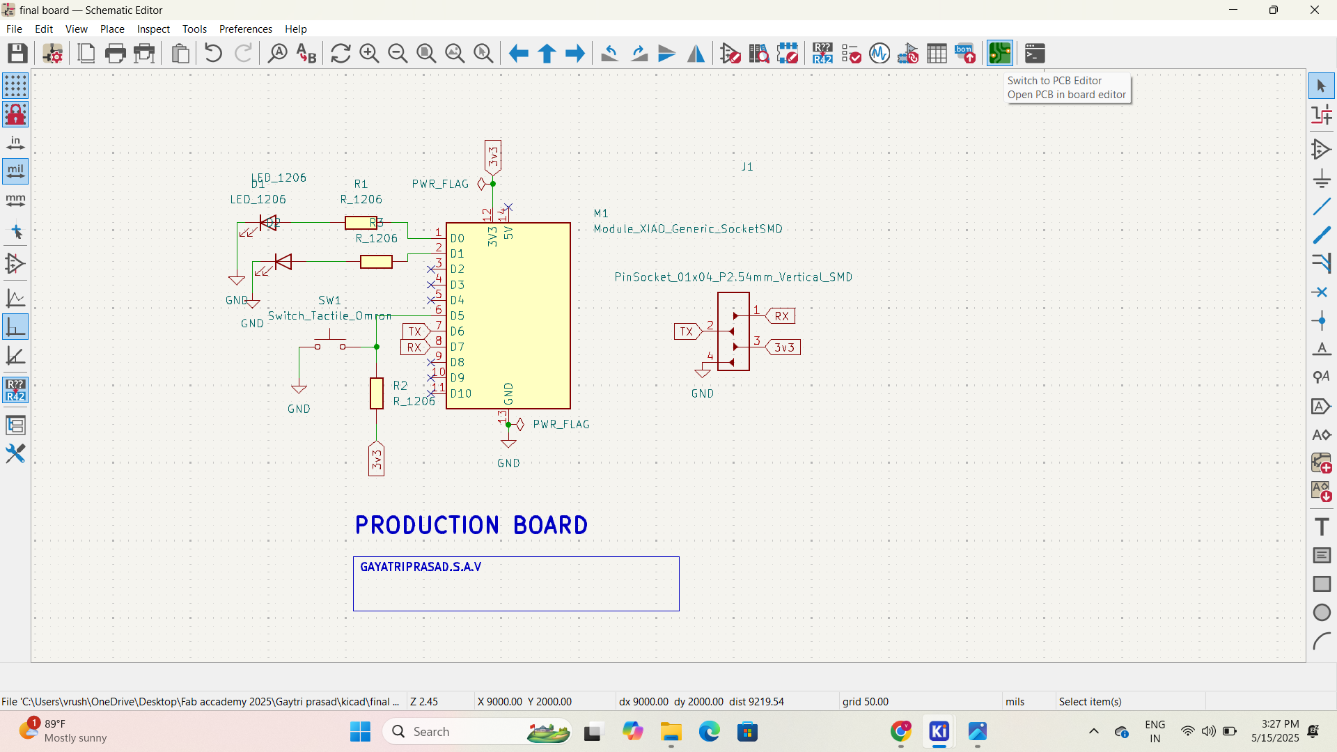
1. Create the KiCad Schematic
- Start a new project in KiCad
- Launch the Schematic Editor
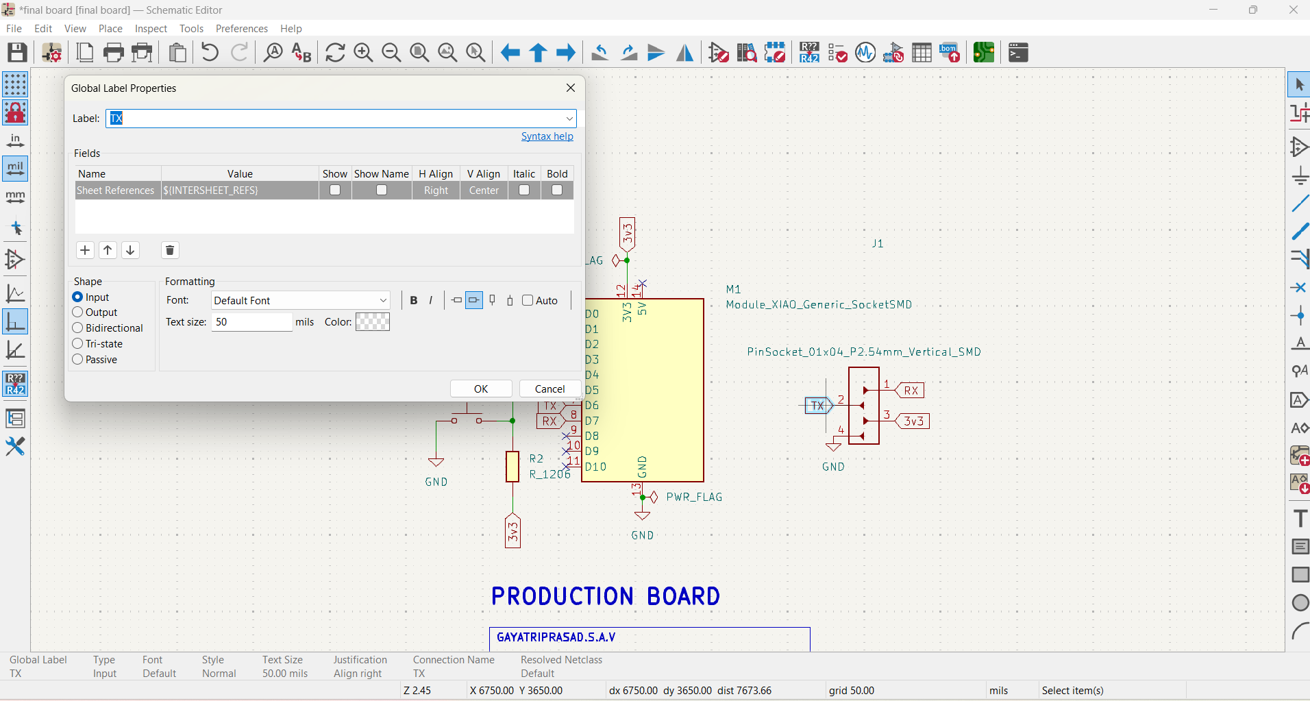
- Add parts ( resistor, LED, button, 6-pin header)
- Annotate schematic
- Assign footprints
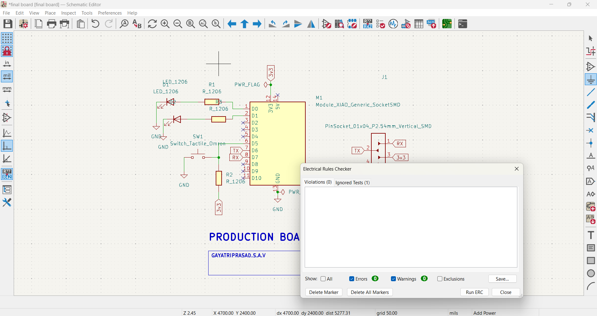
- Perform ERC (Electrical Rules Check)
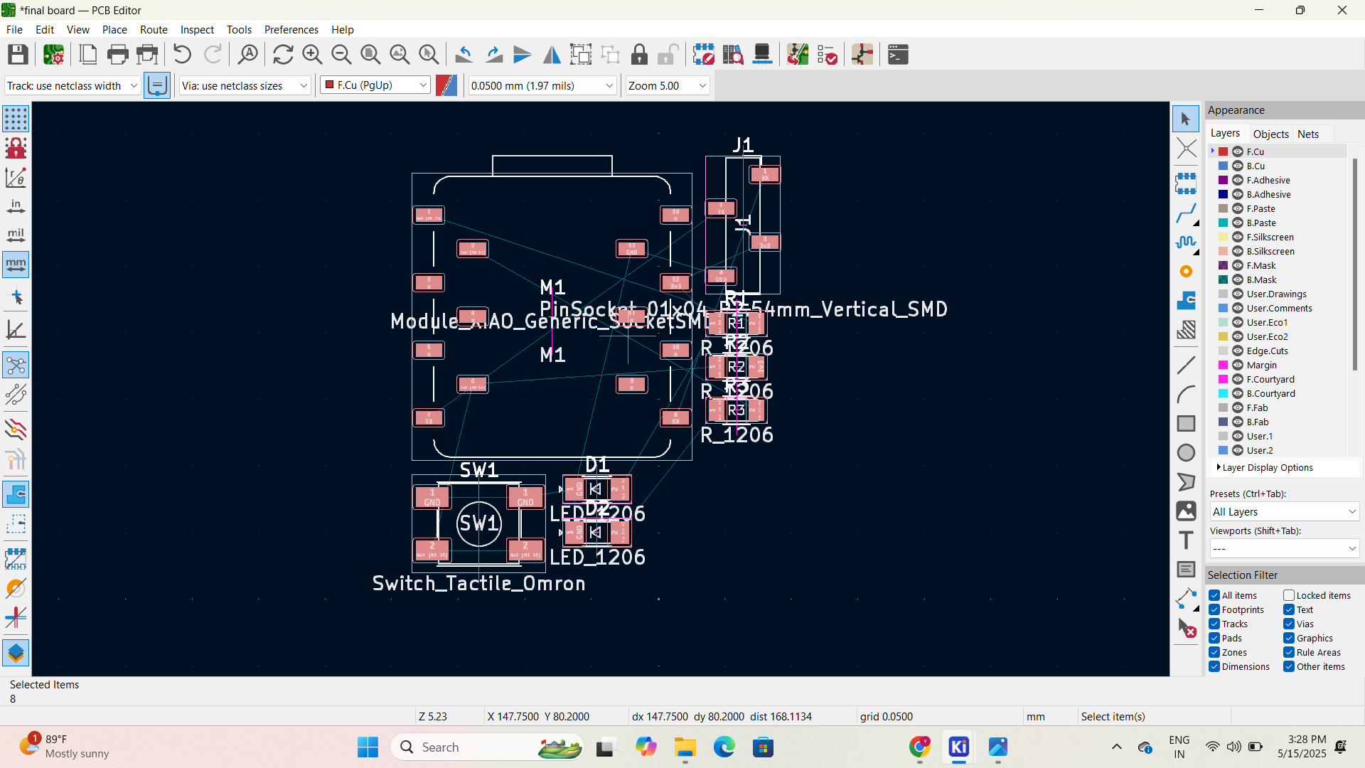
- Complete schematic with labeled components
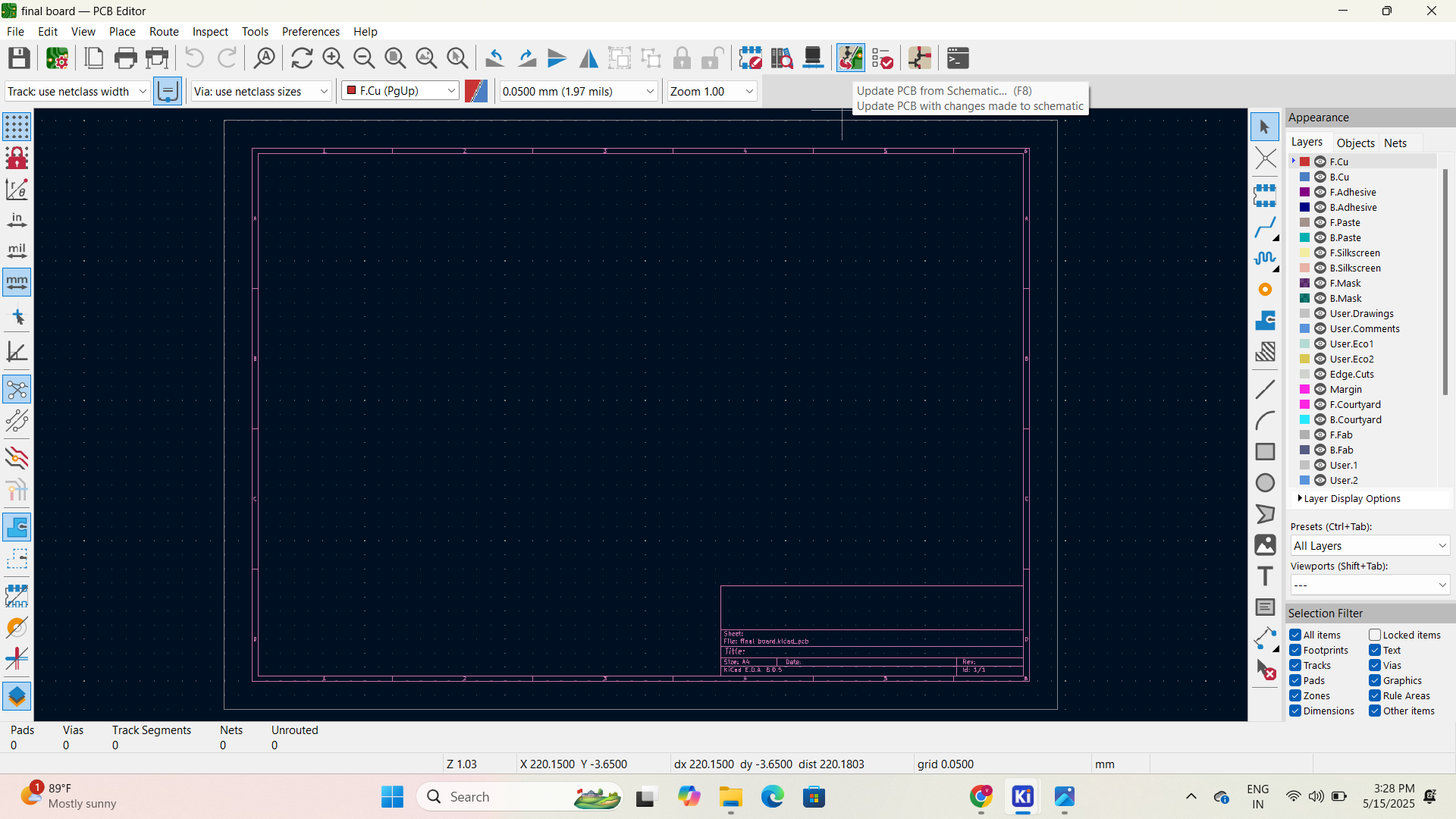
- Open PCB Editor
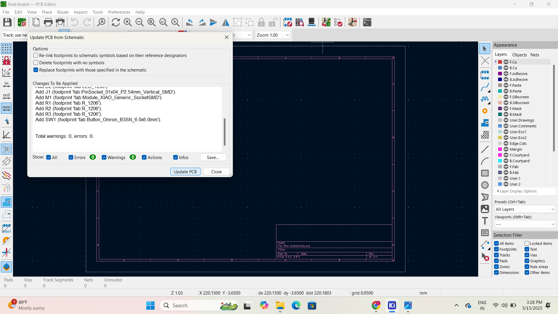
- Update PCB from schematic or import netlist
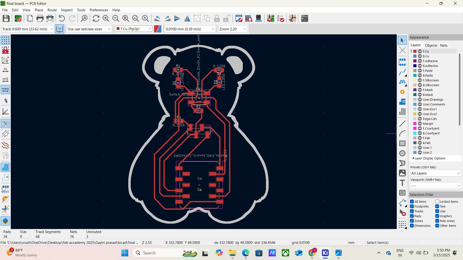
- Final layout with board outline
- DRC results
My Objective
2. KiCad PCB Layout Design
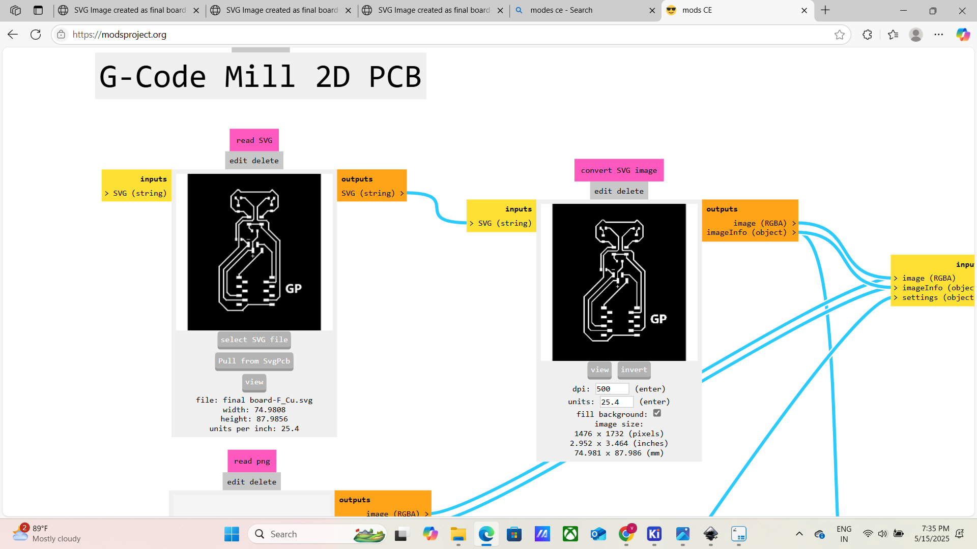
3. Export SVG or Gerber for Milling
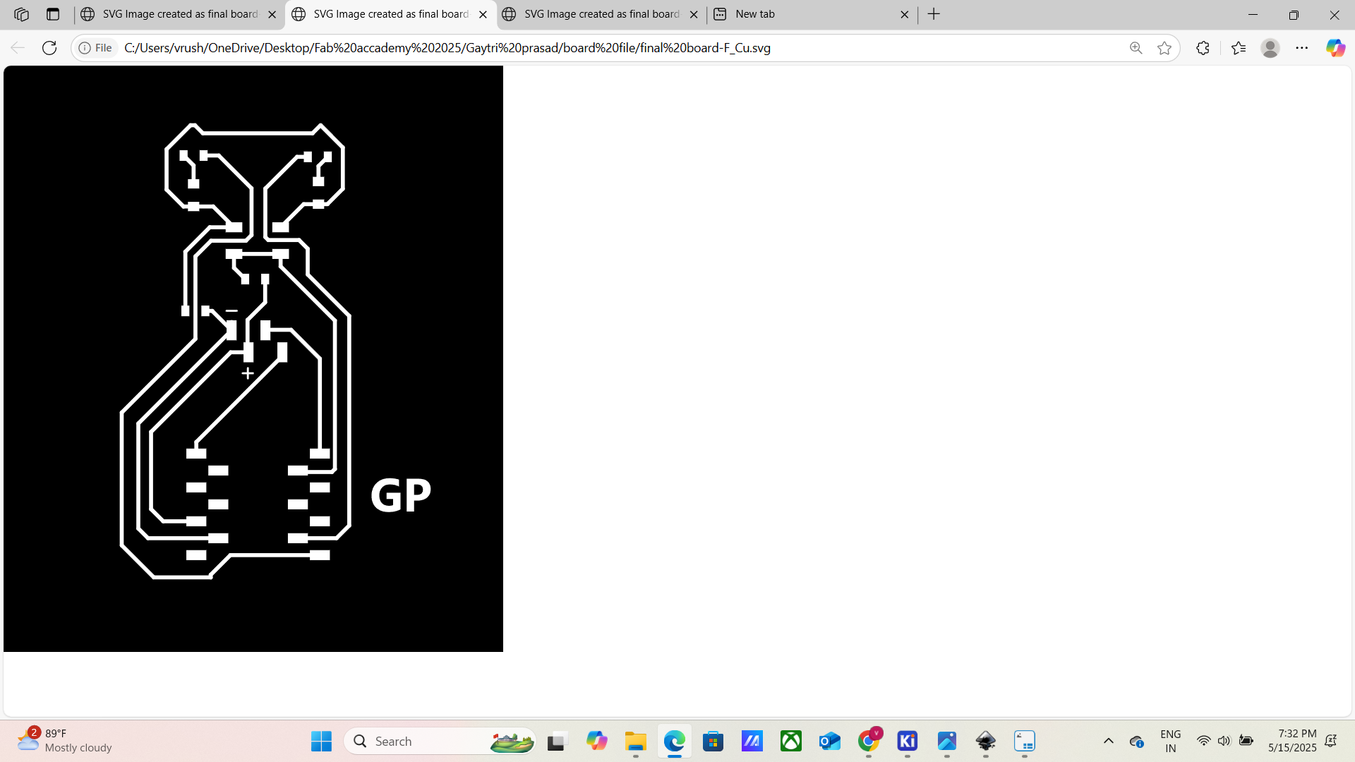
- Plot only top copper layer (F.Cu)
- Export to SVG or PNG at 1000 DPI for mods
- Export edge cuts layer for board outline
- Top copper trace export
- Outline layer export
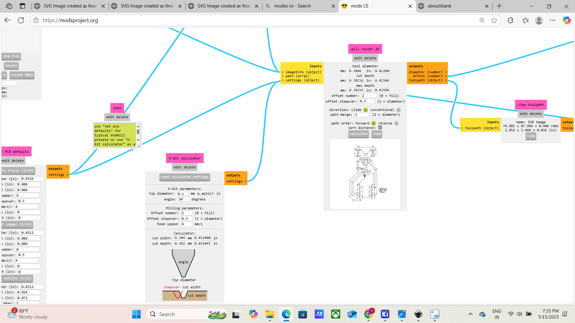
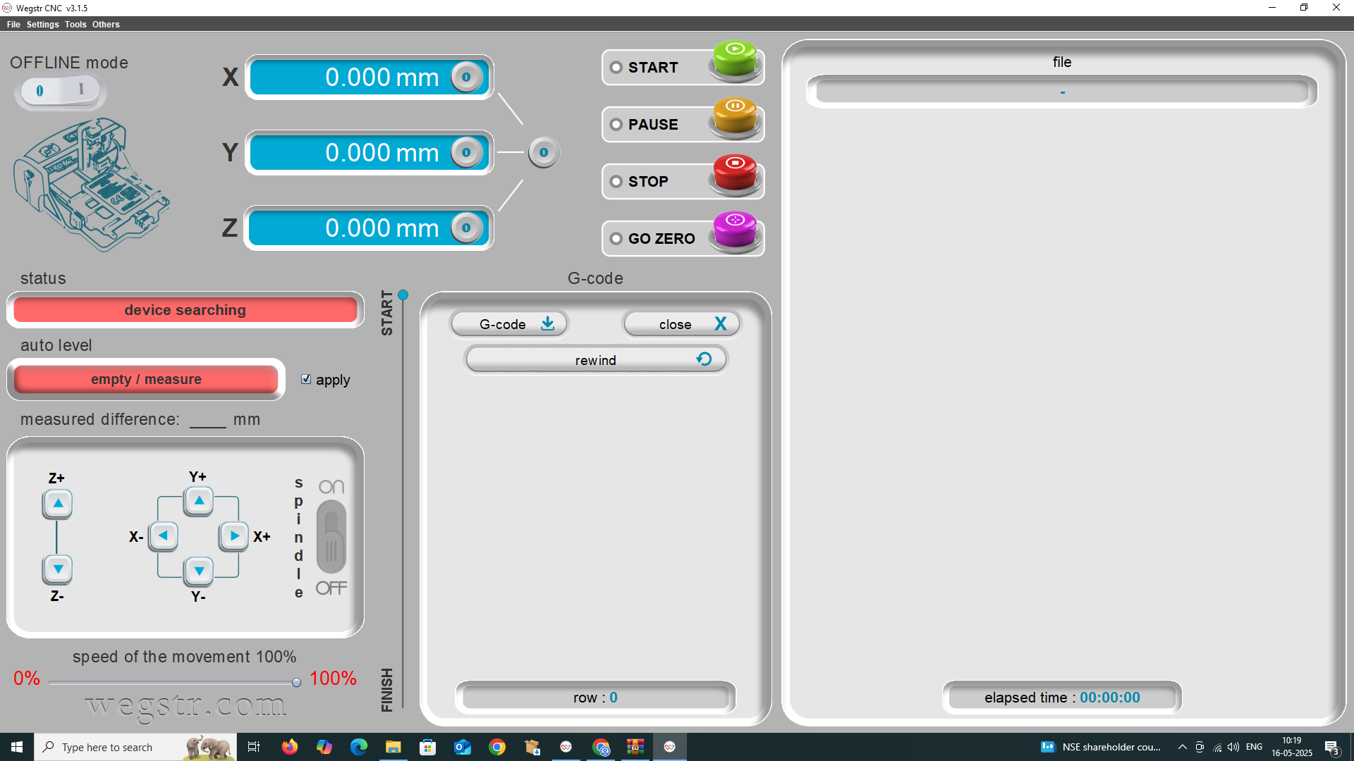
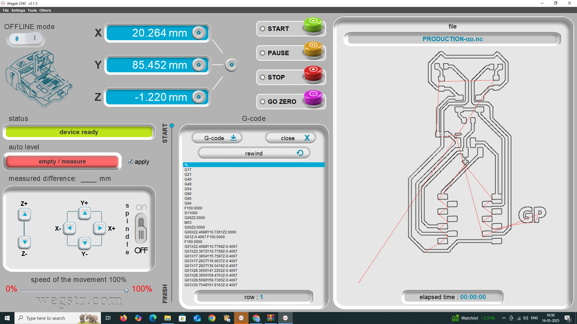
4. Use Mods CE/Fab Modules to Generate Toolpaths
- Load image (traces PNG)
- Select mill traces (1/64")
- Set cut depth: 0.1 mm, max depth: 0.1 mm, tool diameter: 0.4 mm
- Set origin (X=0, Y=0)
- Save the .rml or .nc file
- Repeat for cutout layer with mill outline (1/32")
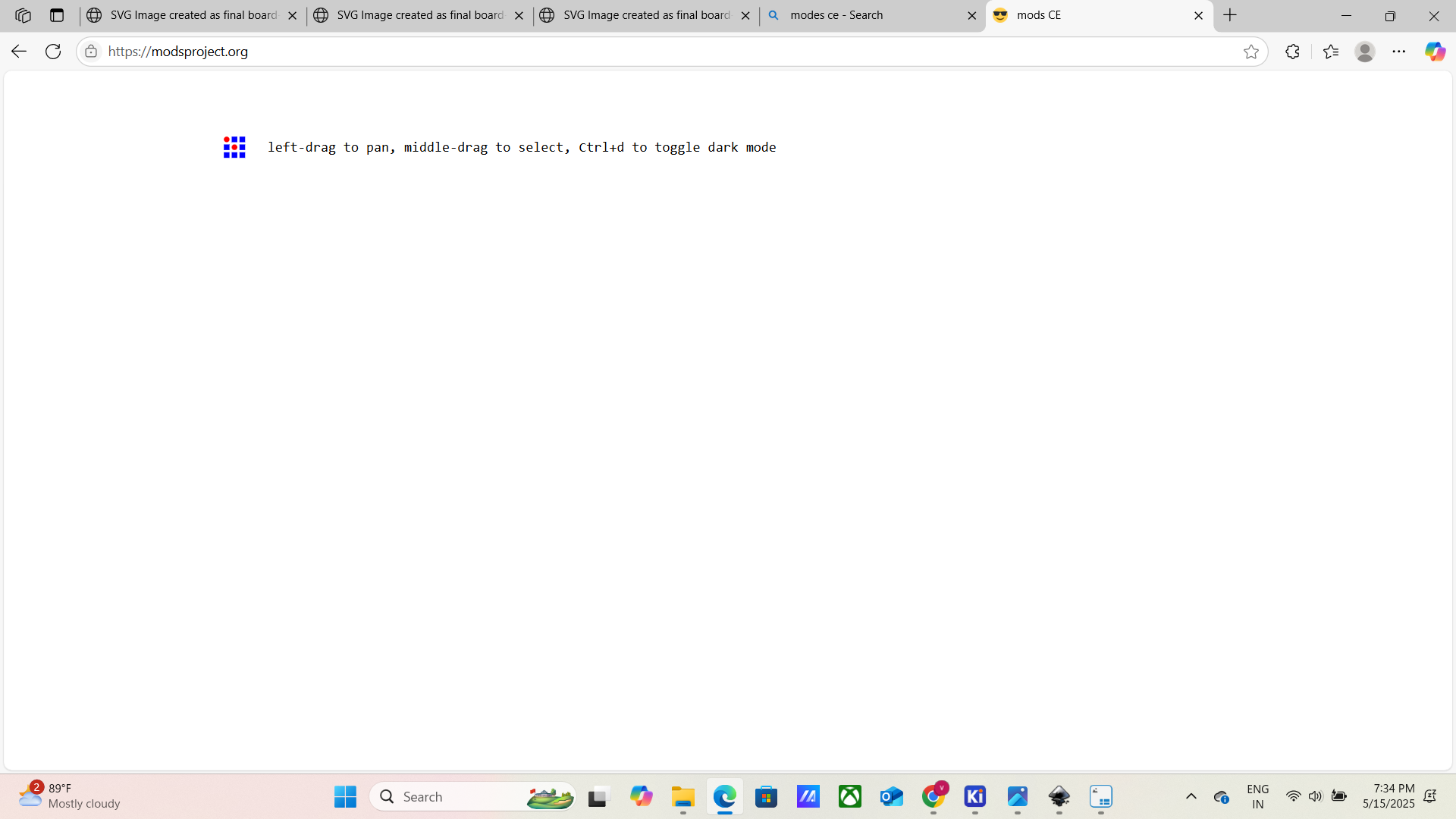
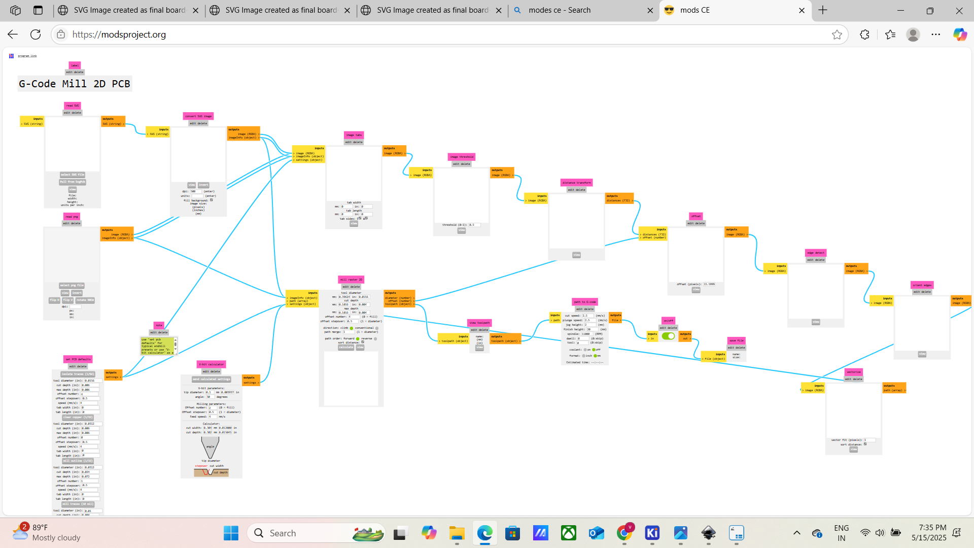
- Mods CE interface with loaded image
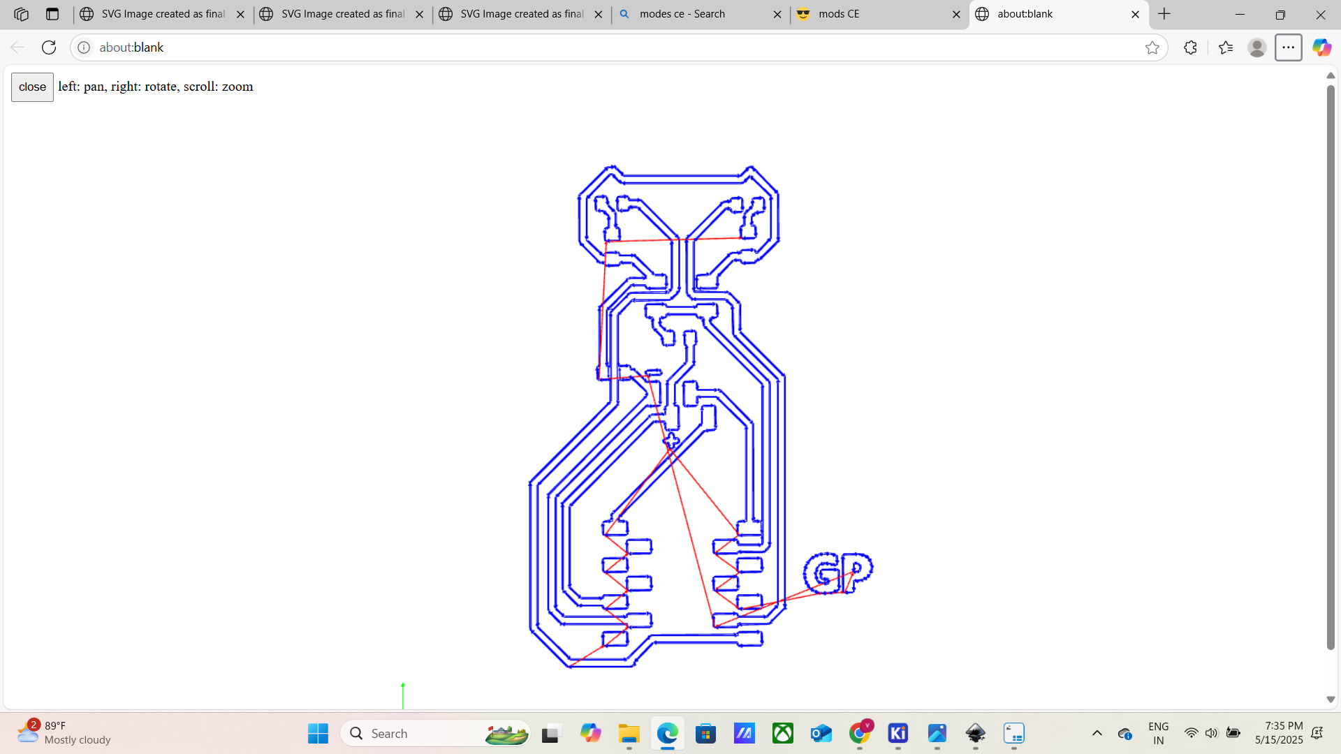
- Toolpath preview for traces
- Toolpath preview for cutout
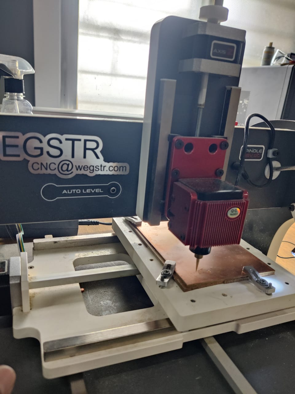
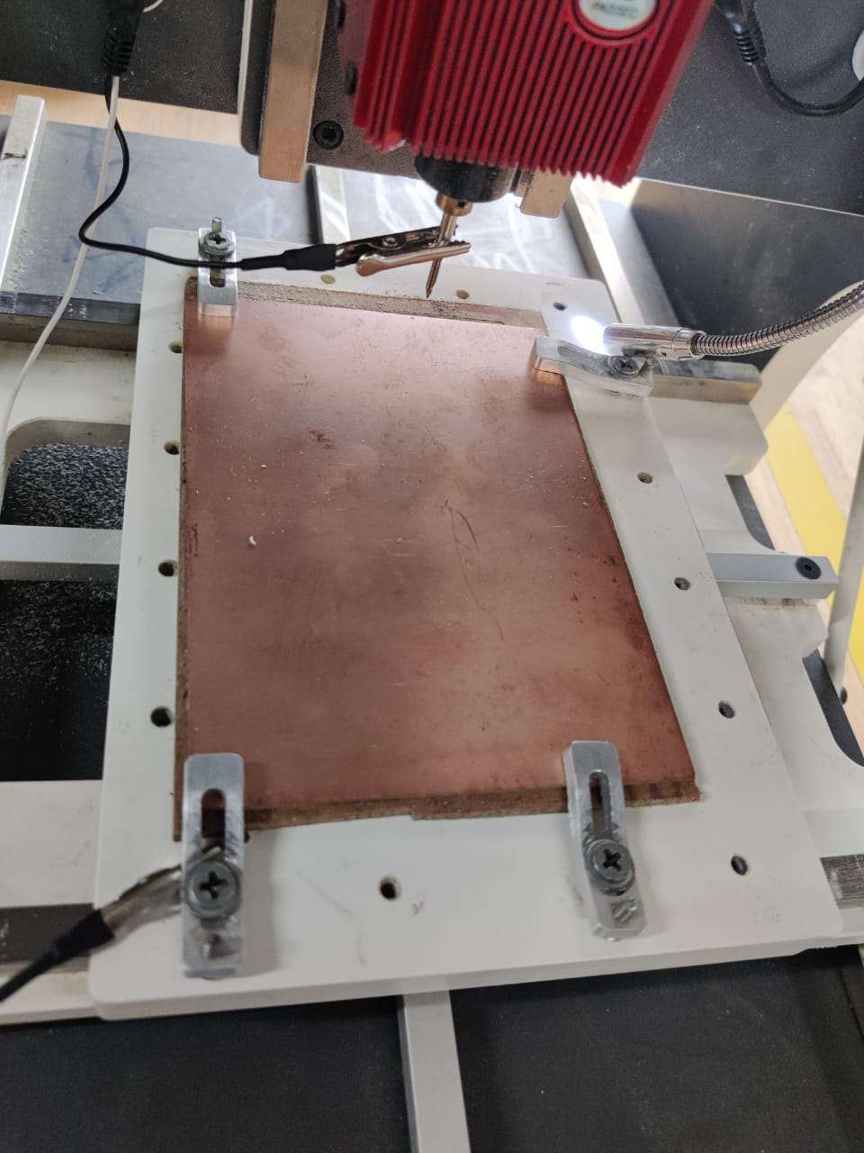
5. Mill the Board
- Secure blank PCB on the CNC bed using tape
- PCB fixed on CNC bed
- Set X, Y, Z origins
- Run the traces toolpath
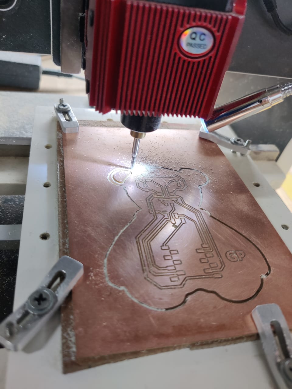
- Change bit and run cutout toolpath
- level the pcb board
 >
>
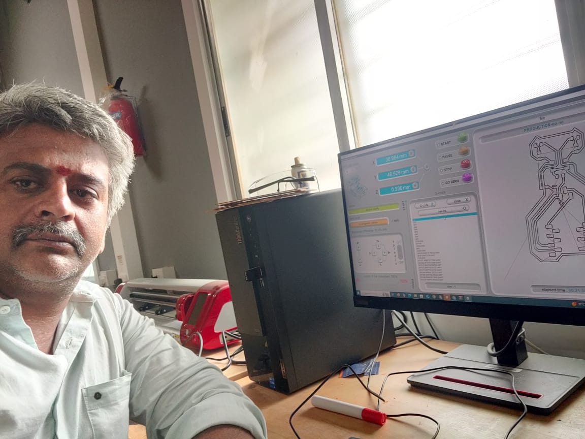
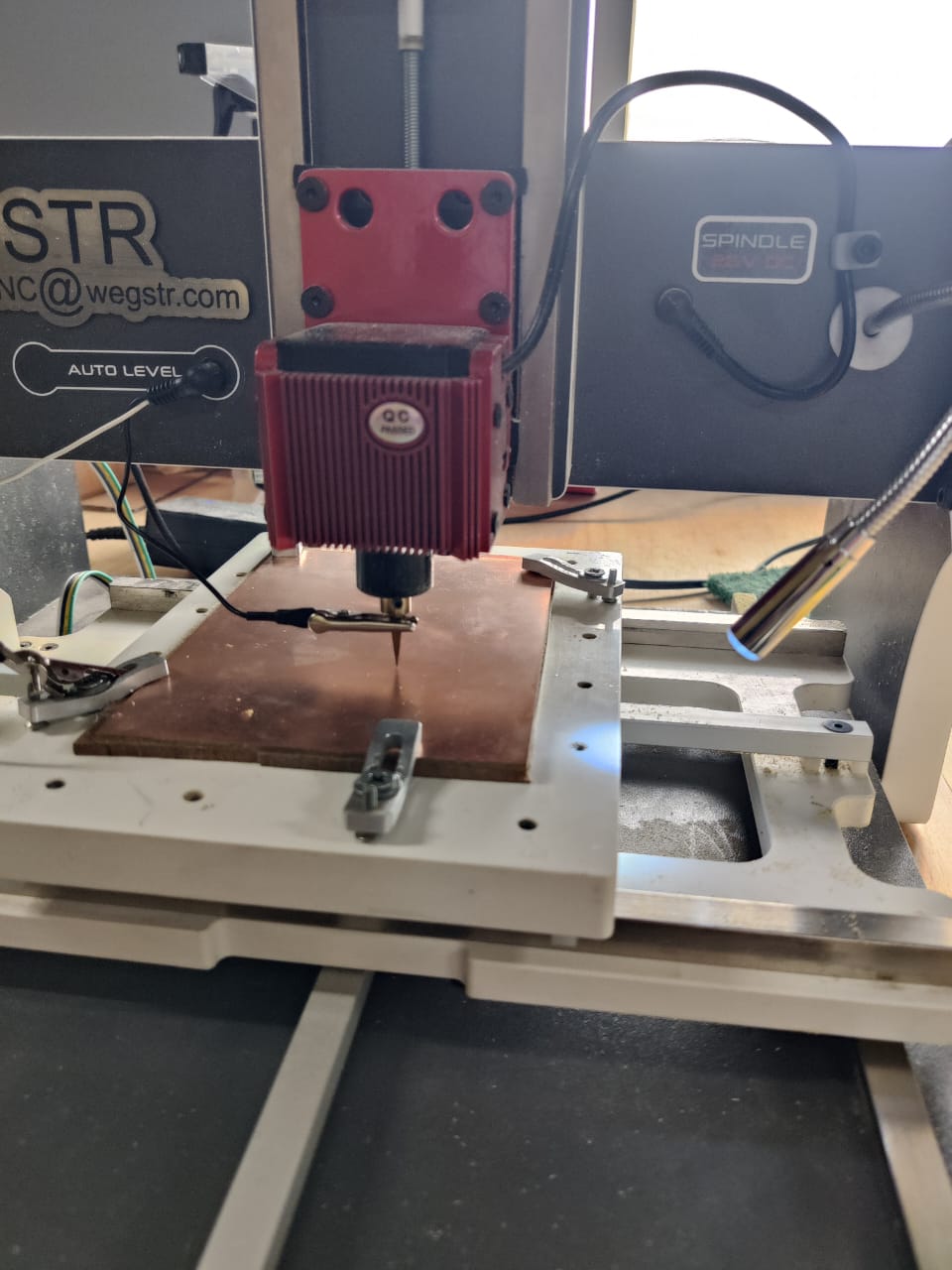
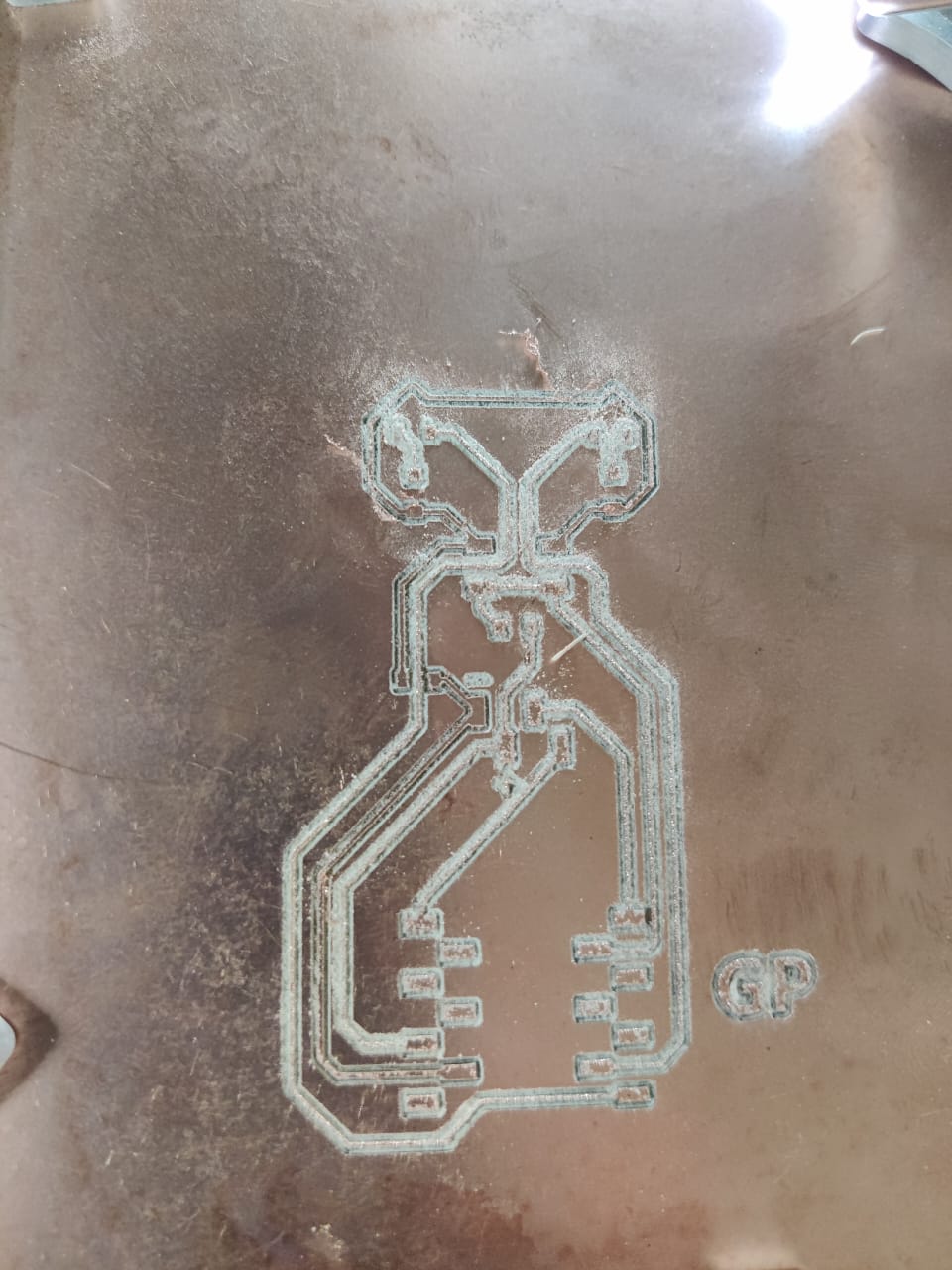
- Milling in progress
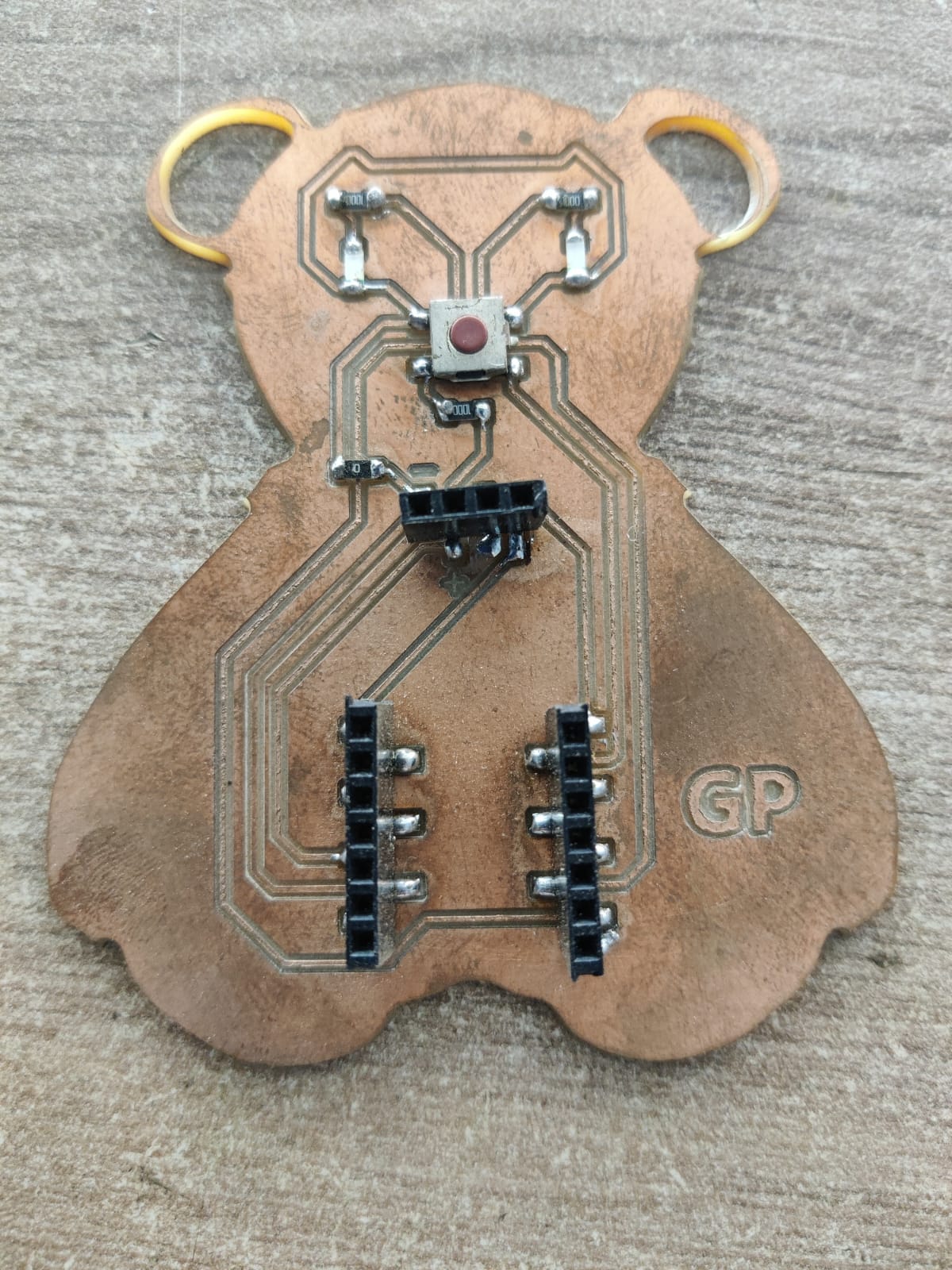
- Final milled PCB board
- Now the circuit is ready
- Now the circuit got edgecut and the board is ready to assemble
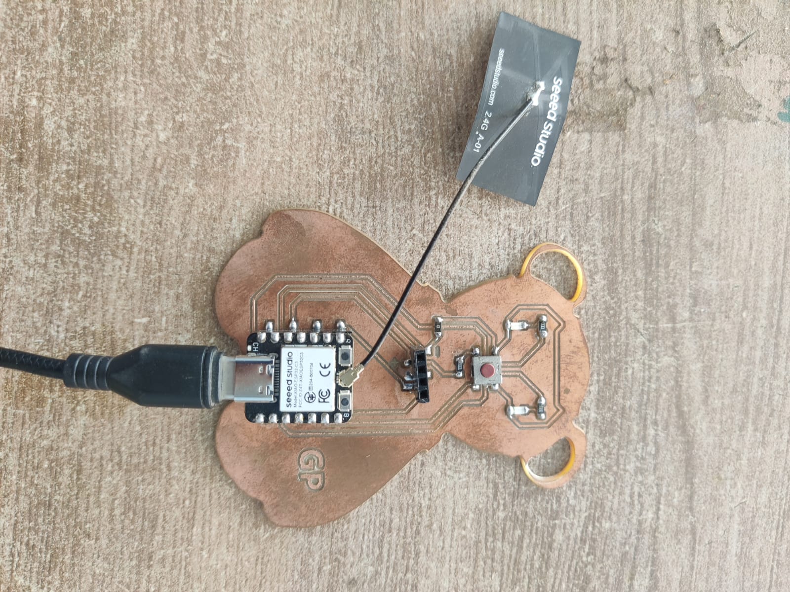
- After the edge cutting process was completed, the PCB was carefully removed from the machine
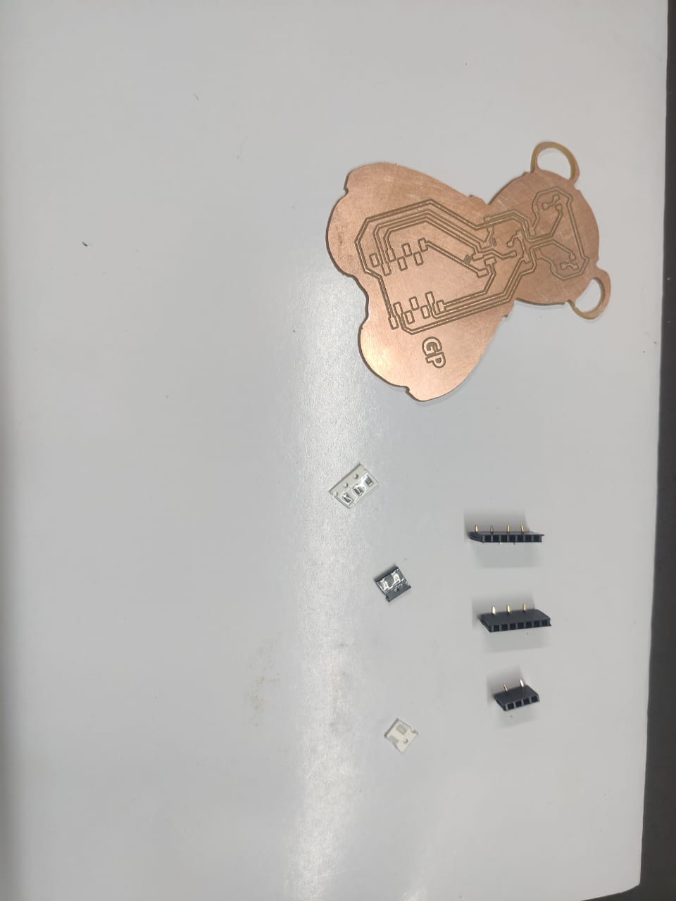
- 1 × Custom Milled Copper PCB – Single-sided copper-clad board designed and fabricated using PCB milling.
- 1 × SMD Tactile Push Button Switch – Used as a user input switch for triggering functions or resetting the circuit.
- 4 × SMD Resistors – Used for current limiting, pull-up, or pull-down functions in the circuit.
- 1 × 4-Pin Female Header – Used for programming, communication, or external connections.
- 2 × 6-Pin Female Headers – Used for mounting and interfacing a microcontroller module or expansion board.
- Copper Traces – Milled conductive paths that electrically connect all components on the PCB.
PCB Assembly Description
The PCB was designed in KiCad and milled from a single-sided copper-clad board. The circuit consists of a tactile push button switch, four surface-mount resistors, and female header connectors for interfacing with external modules. The custom teddy-bear-shaped PCB was fabricated using a PCB milling machine and assembled through soldering of all electronic components. The headers provide a removable connection for a microcontroller board, while the push button acts as the primary user input device.
🔌 6. Solder the Components
- Use flux and tweezers for SMD soldering
- Test each connection with multimeter
- Optionally test ISP or UART communication
- Soldering in progress
- Fully assembled board
- Multimeter testing
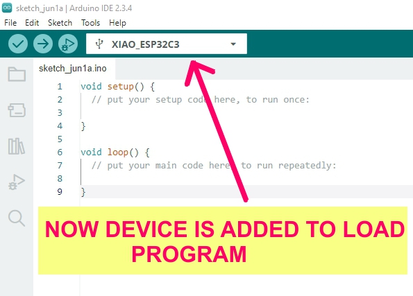
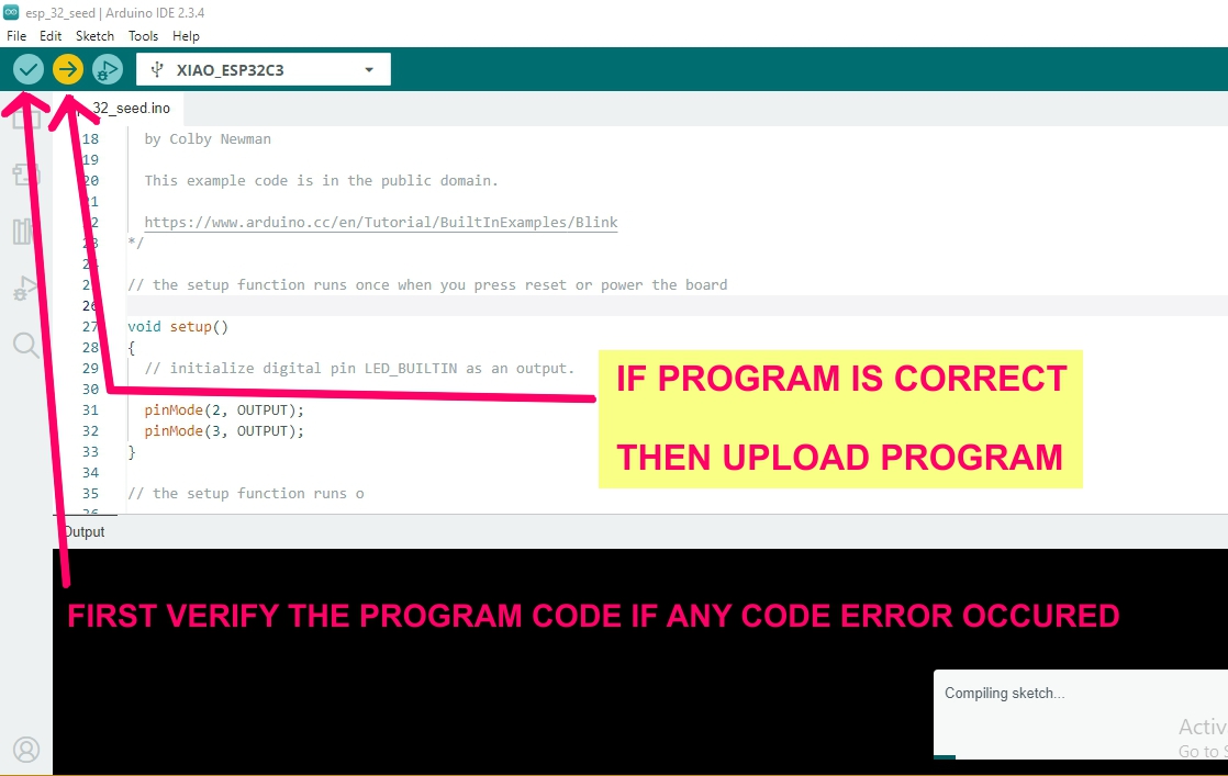
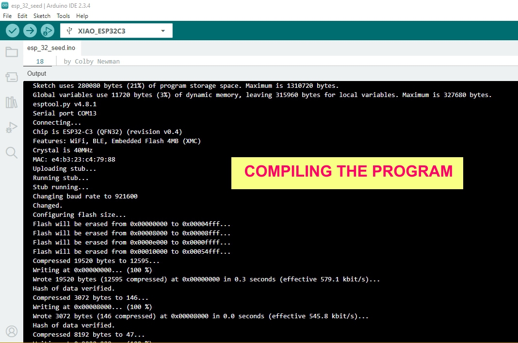
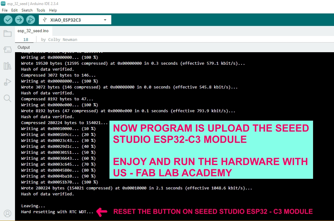
7. Configure and Examine the Board
- Connect with USB-to-UART or ISP programmer
- Burn bootloader or test blinking code
- Use terminal to check serial response (if available)
- Board connected to computer
- Terminal output (if serial used)
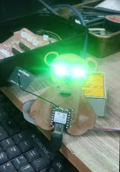
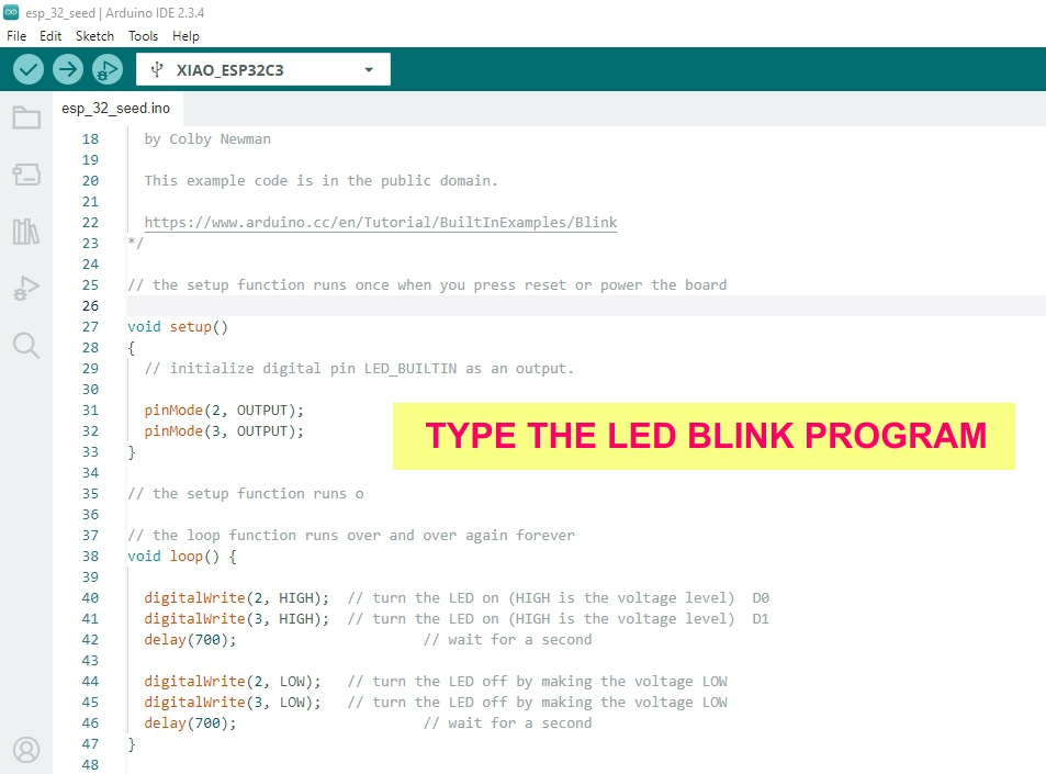
- LED blinking Programming
- // the setup function runs once when you press reset or power the board
- void setup() {
pinMode(2, OUTPUT);
pinMode(3, OUTPUT);
} - // the loop function runs over and over again forever
- void loop() {
digitalWrite(2, HIGH); // turn the LED on
digitalWrite(3, HIGH);
delay(700);
digitalWrite(2, LOW); // turn the LED off
digitalWrite(3, LOW);
delay(700);
}


ul class="code-steps"
Summary Checklist for Documentation
| Stage | sScreenshot |
|---|---|
| Schematic | Full circuit & ERC check |
| PCB Layout | Routing + DRC pass |
| Toolpath | Mods/FabModules preview |
| Milling | Process + Finished PCB |
| Assembly | Soldering + Finished board |
| Testing | Programming + Output |