Group Assignment:
Group Assignment Summary – Electronic Design
As part of the group assignment, we used various electronic test equipment available in the lab to observe and analyze the operation of a microcontroller circuit board. We measured voltage, continuity, and signal behavior using tools such as a multimeter and oscilloscope. The multimeter was used to verify power supply levels and check electrical connections, while the oscilloscope was used to visualize digital signals and observe waveform characteristics generated by the microcontroller. Through this hands-on testing and analysis, we gained practical experience in debugging electronic circuits, understanding signal behavior, and validating the proper operation of microcontroller-based systems. This activity strengthened our knowledge of electronic measurement techniques and circuit troubleshooting.
Individual assignment:
Hero Shot
Use an EDA tool to design a development board that uses parts from the inventory to interact and communicate with an embedded microcontroller
Learning outcomes
Select and use software for circuit board design
Demonstrate workflows used in circuit board design
What is EDA tool?
An EDA tool, or Electronic Design Automation tool, is a software or hardware tool used to design and test
electronic
systems. EDA tools are also known as electronic computer-aided design (ECAD) tools.
What EDA tools do?
Design: Create circuit designs
Model: Create models of circuit designs
Simulate: Predict the results of circuit designs before testing
Test: Test the correctness of designs
Analyze: Analyze circuit designs
What are EDA tools used for?
Designing integrated circuits (ICs)
Designing printed circuit boards (PCBs)
Designing systems for data communications, the internet, transportation, and consumer devices
How do EDA tools help?
Increase productivity
Improve power, performance, and area (PPA)
Reduce time to market (TTM)
Anticipate chip performance
Assemble circuit elements
Predict circuit behavior
Basic electronics

Capacitors (C) – Store and release electrical energy. Measured in farads (F).

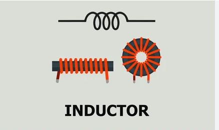
Inductors (L) – Store energy in a magnetic field when current passes through. Measured in henries (H).
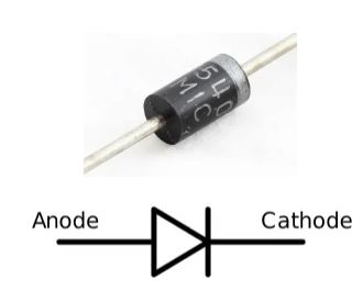
Diodes (D) – Allow current to flow in only one direction.
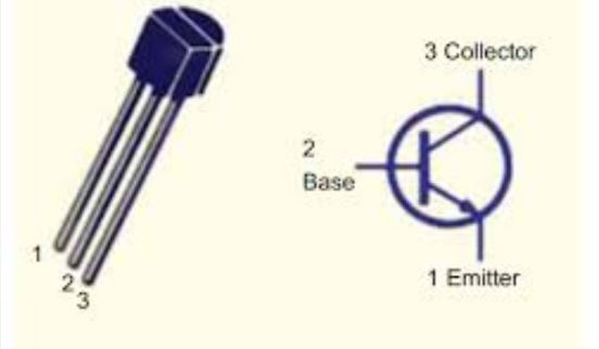
2. Active Components These components require a power source to function. Transistors (Q) – Act as switches or amplifiers. Types: Bipolar Junction Transistor (BJT) and Field Effect Transistor (FET).
Operational Amplifiers (Op-Amps) – Used for signal amplification, filtering, and other functions.

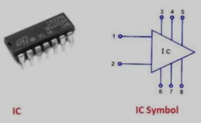
Integrated Circuits (ICs) – Contain multiple electronic components within a single package, like microcontrollers or logic gates.
3. Electromechanical Components Switches (S) – Manually or electronically control the circuit's on/off state.

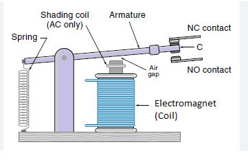
Relays – Electrically operated switches that use electromagnets.
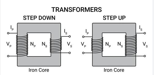
Transformers – Transfer electrical energy between circuits through electromagnetic induction.

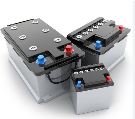
4. Power Components Batteries – Store and supply DC power.
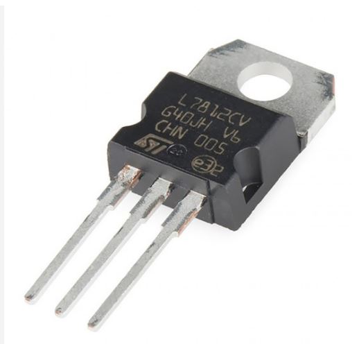
Voltage Regulators – Maintain a stable voltage supply.
Transformers – Step up or step down AC voltage.
5. Sensors & Display Components LEDs (Light Emitting Diodes) – Emit light when current flows through them.

LCD/OLED Displays – Show information in digital circuits.

Temperature, Pressure, and Motion Sensors – Detect changes in the environment and provide input to circuits.
Weekly Goal: Development Board
>The XIAO ESP32S3 is a compact yet powerful development board developed by Seeed Studio, based on the Espressif ESP32-S3 SoC. It is part of Seeed’s XIAO series, known for their small footprint and versatile functionality. Here’s a concise description with key features:
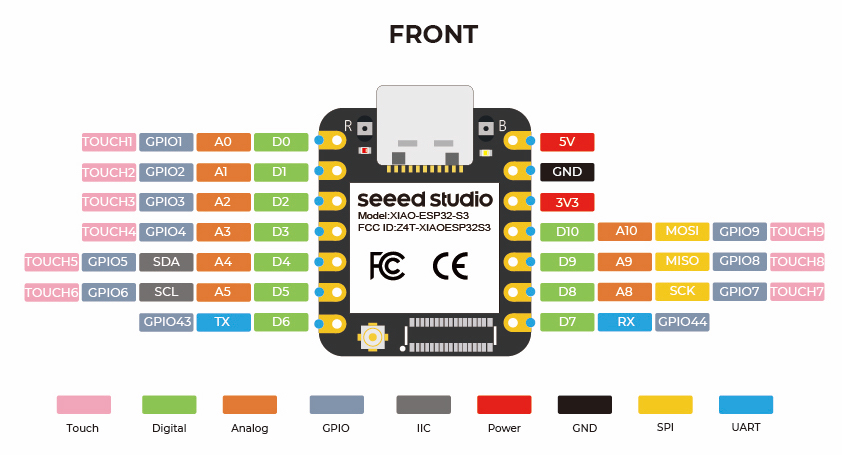
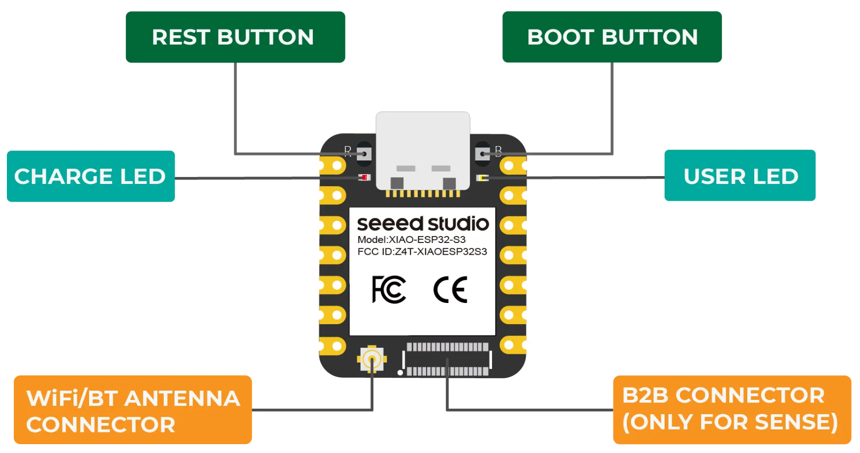
XIAO ESP32S3 Overview Hardware Specifications
| Category | Details |
|---|---|
| Flash & PSRAM | 8 MB Flash 8 MB PSRAM |
| Wireless Connectivity | Wi-Fi 802.11 b/g/n Bluetooth® 5 (LE) |
| USB Support | Native USB-C (supports USB OTG, device and host modes) |
| Form Factor | Extremely compact: 21 × 17.5 mm Compatible with XIAO series shields |
| GPIOs | 11 multifunctional GPIOs Supports ADC, SPI, I2C, UART, PWM, and DAC |
| Camera Interface | Dedicated 8-bit parallel camera interface (DVP) Suitable for AI and vision applications |
| AI Capability | Supports TensorFlow Lite, ESP-DL, and other AI frameworks on edge |
| Operating Voltage | 3.3V logic level |
| Power Supply | USB-C or 5V input through pins |
| Battery Support | Built-in battery charging circuit (Li-Po charging via USB-C) |
| Ideal For |
- Wearable and IoT applications - Edge AI (e.g., simple image classification, gesture recognition) - DIY embedded projects with space constraints - USB-enabled devices or HID applications |
PCB Design Using KiCad
Overview of KiCad
KiCad is an open-source EDA (Electronic Design Automation) tool used for schematic capture and PCB layout. A typical KiCad project includes various files such as:
- Project file (
.proor.kicad_pro) - Schematic file (
.sch) - PCB layout file (
.kicad_pcb) - Supporting libraries (symbols, footprints)
- Optional: simulation files, BOMs, and netlists
Designing the Development Board
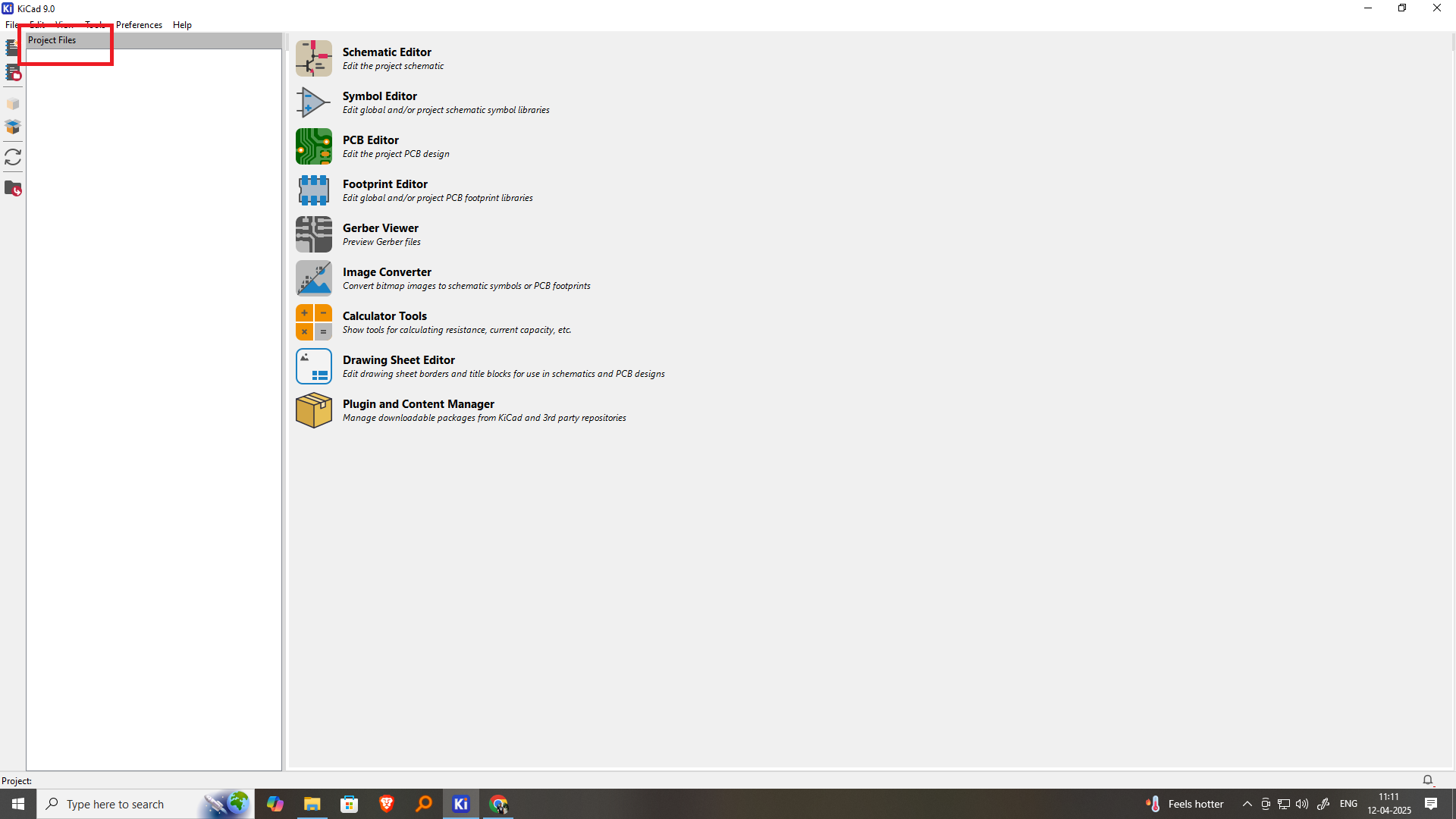
KiCad Software Installation
- I downloaded KiCad PCB design software from the official KiCad website.
- Visited the download page:https://www.kicad.io/download
- Selected the Windows operating system and downloaded the latest stable release compatible with my computer.
- After the download was completed, I opened the installer file.
- Followed the installation wizard and selected the default installation options.
- Installed the required libraries and 3D component packages included with KiCad.
- Completed the installation and launched KiCad successfully.
- Verified that the Schematic Editor, PCB Editor, Footprint Editor, and 3D Viewer were working properly.
- KiCad was then used throughout my Fab Academy assignments for schematic design, PCB layout, and generating fabrication files.
Schematic Design Process
The first step in the workflow is creating a schematic. This involves:
- Selecting components from standard or custom libraries
- Connecting components with wires to define electrical relationships
- Annotating components for clarity and organization
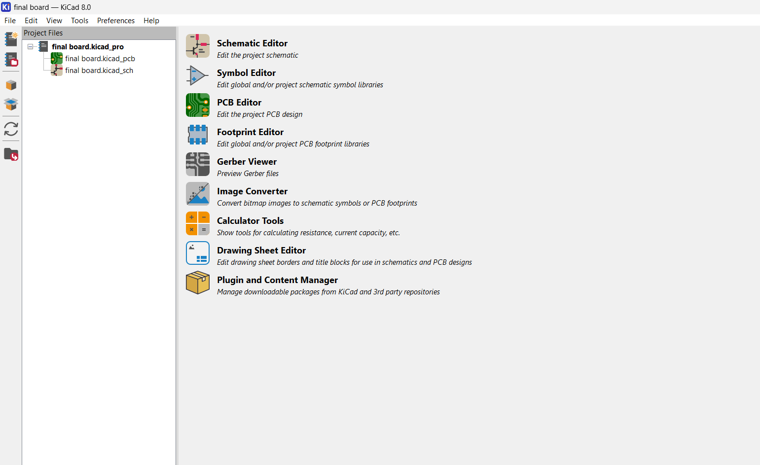
Create a New Project
Open KiCad → Click on “File > New Project”.
Choose a name and location for your project.
2. Schematic Design (Eeschema)
Open Schematic Editor.
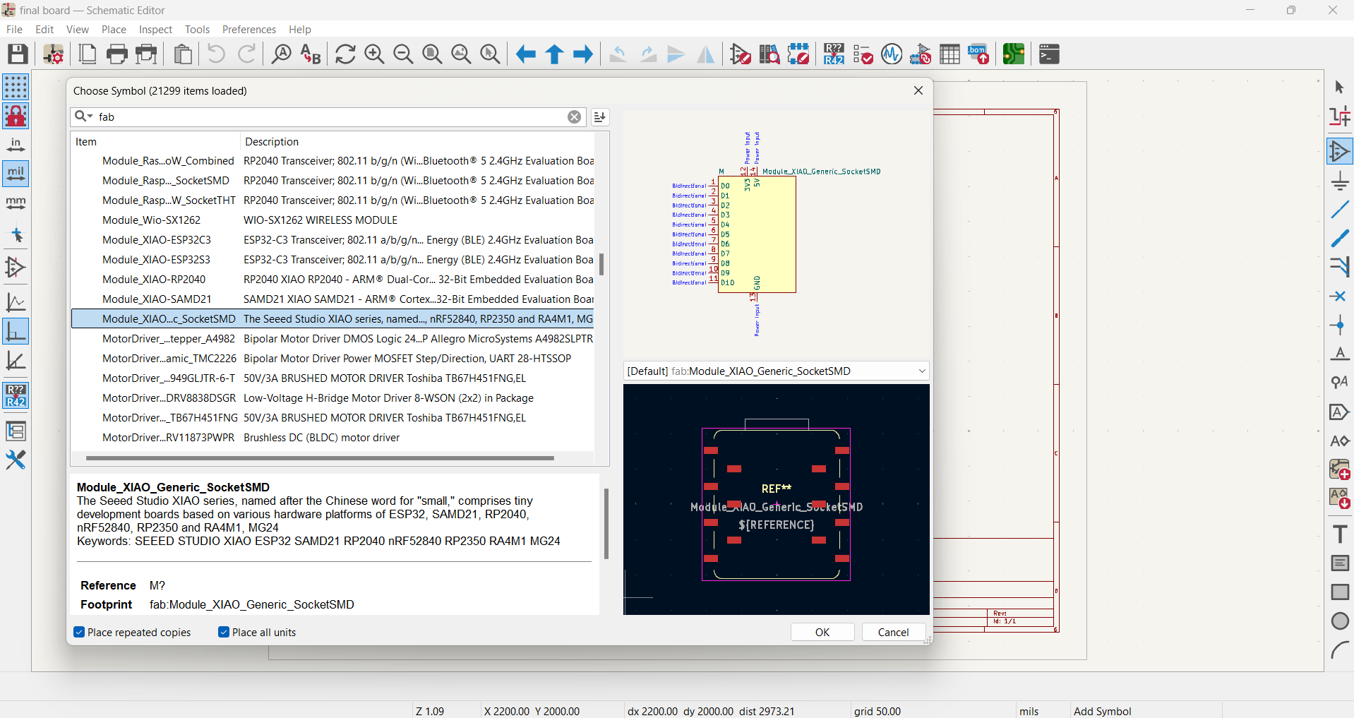
Place components using the “Place Symbol” tool.
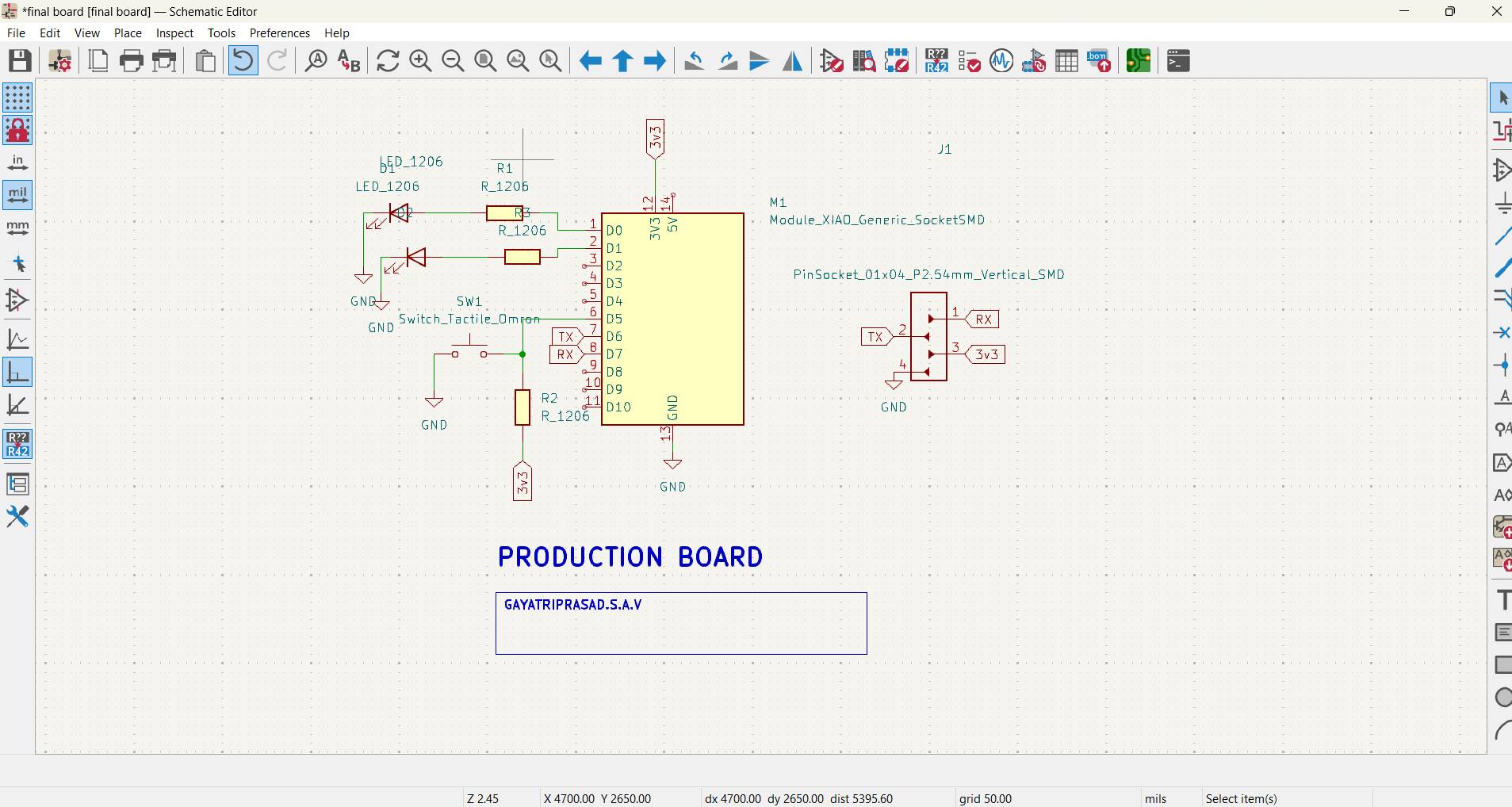
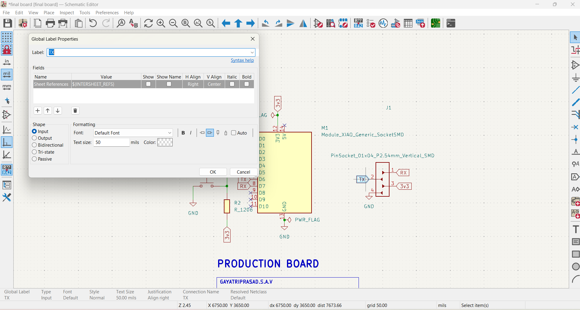
Wire the components using the “Place Wire” tool.
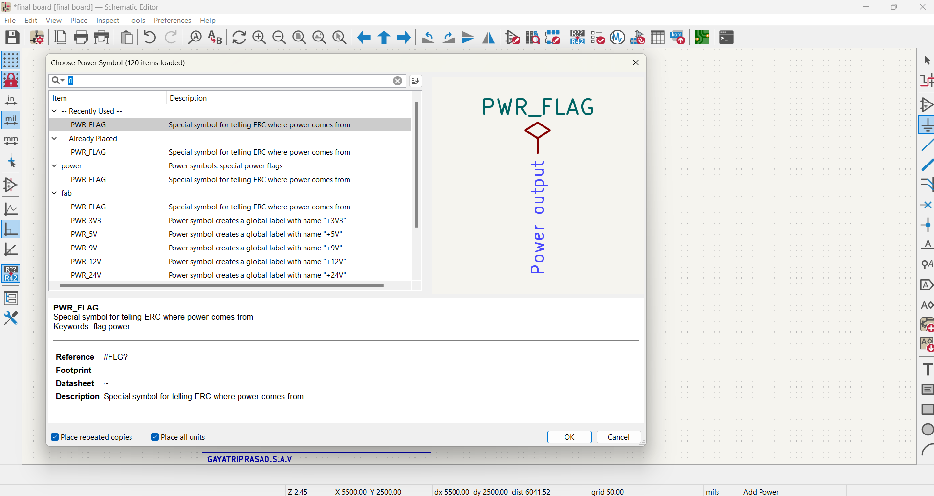
Add power and ground symbols where needed.
3. Assign Footprints
Open “Assign PCB Footprints” tool.
Match each symbol to its appropriate footprint (e.g., resistor to 0603 footprint).
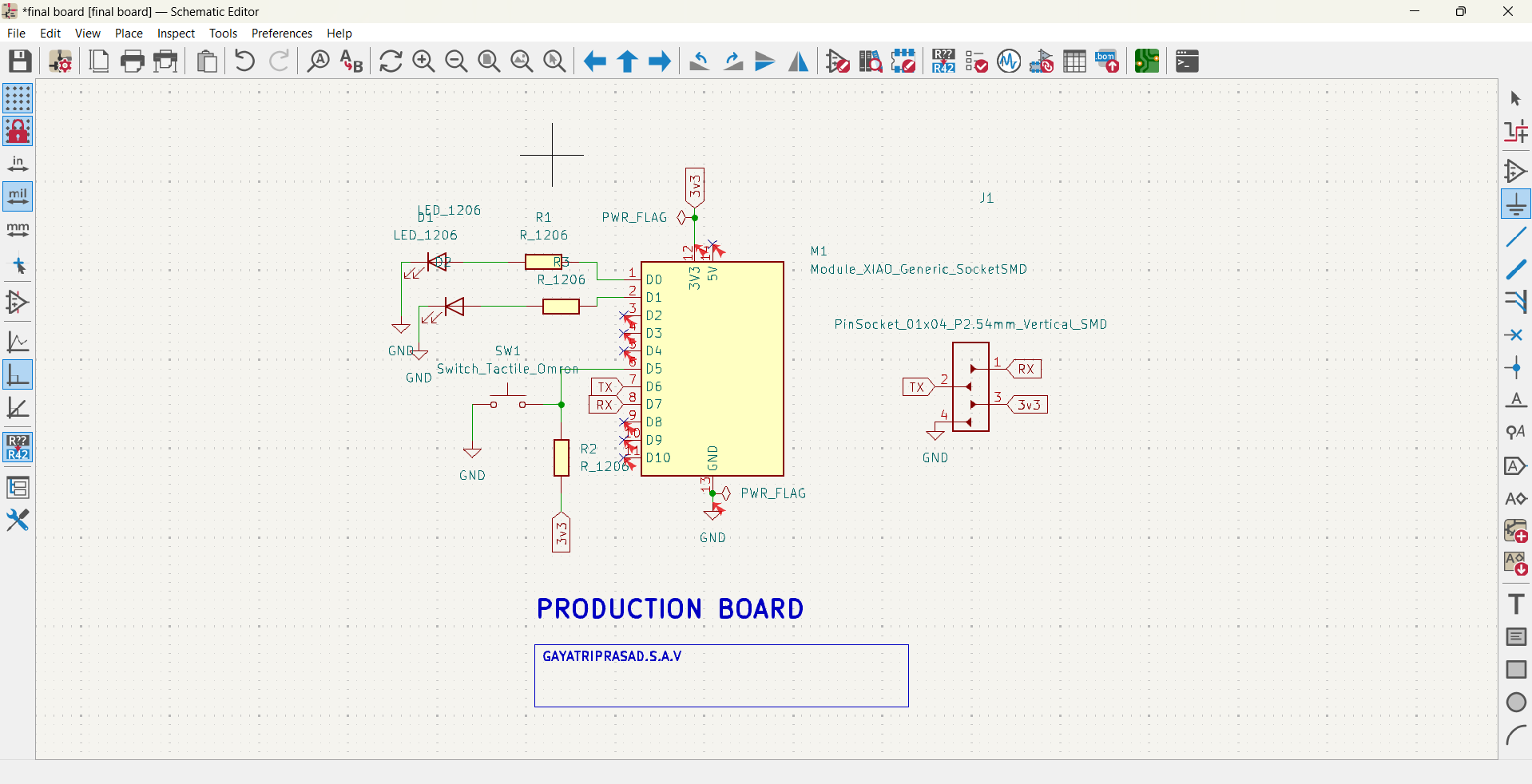
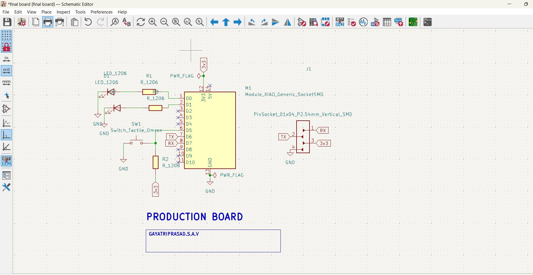
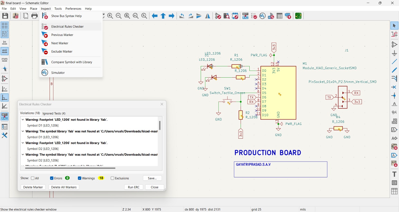
4. Electrical Rules Check (ERC)
Run ERC to check for missing connections or issues.
Fix warnings/errors if needed.
- Assign Footprints: Link each schematic symbol to a corresponding physical footprint.
- Electrical Rules Check (ERC): Run ERC to verify all connections and catch potential schematic errors.
- Generate Netlist / Update PCB: Click “Update PCB from Schematic” to transfer schematic data to the PCB layout editor.
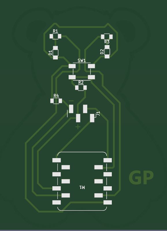
- PCB Layout (Pcbnew):
Fix warnings/errors if needed.
• Open the PCB editor
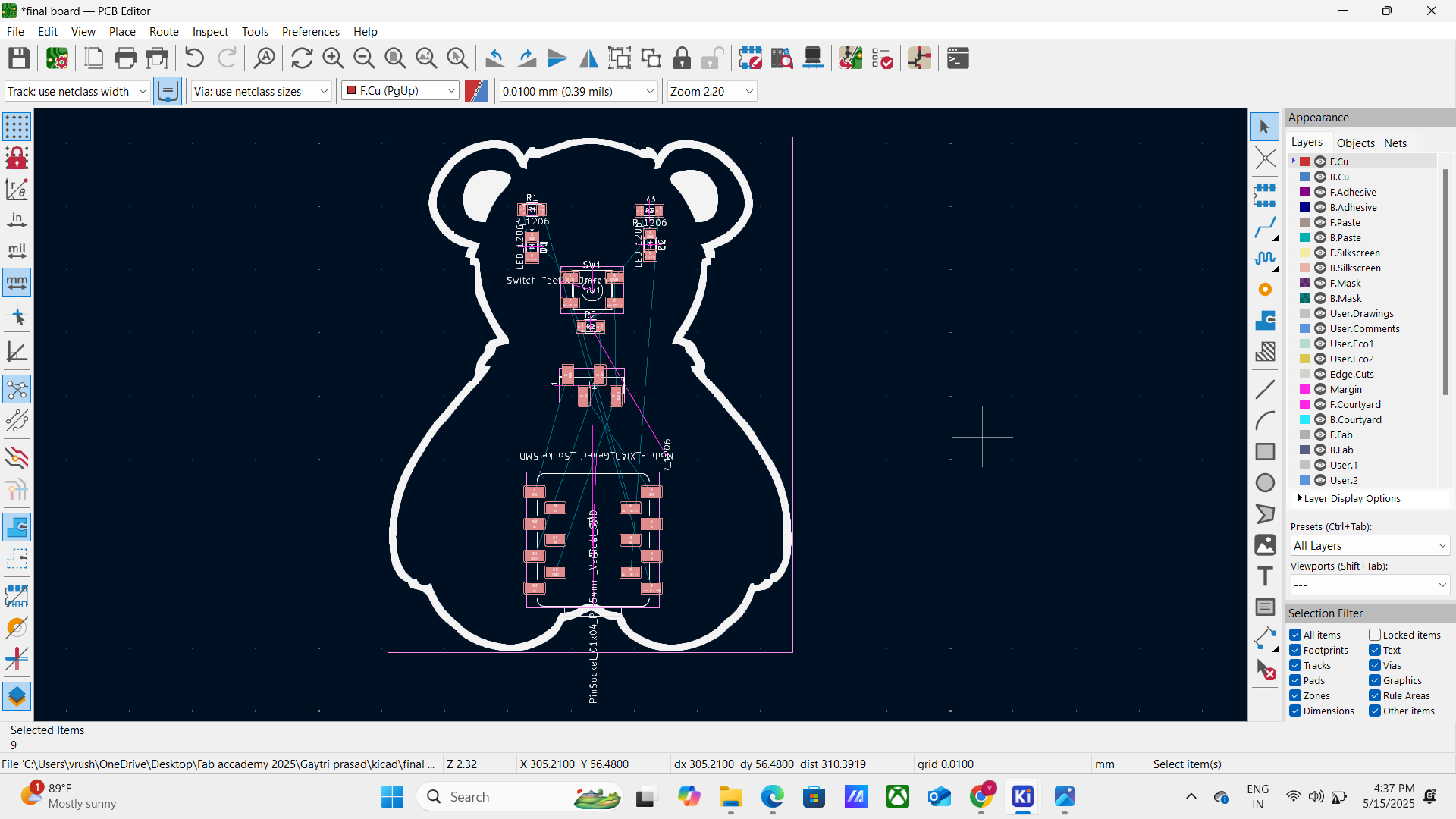
• Import component footprints
• Arrange components logically
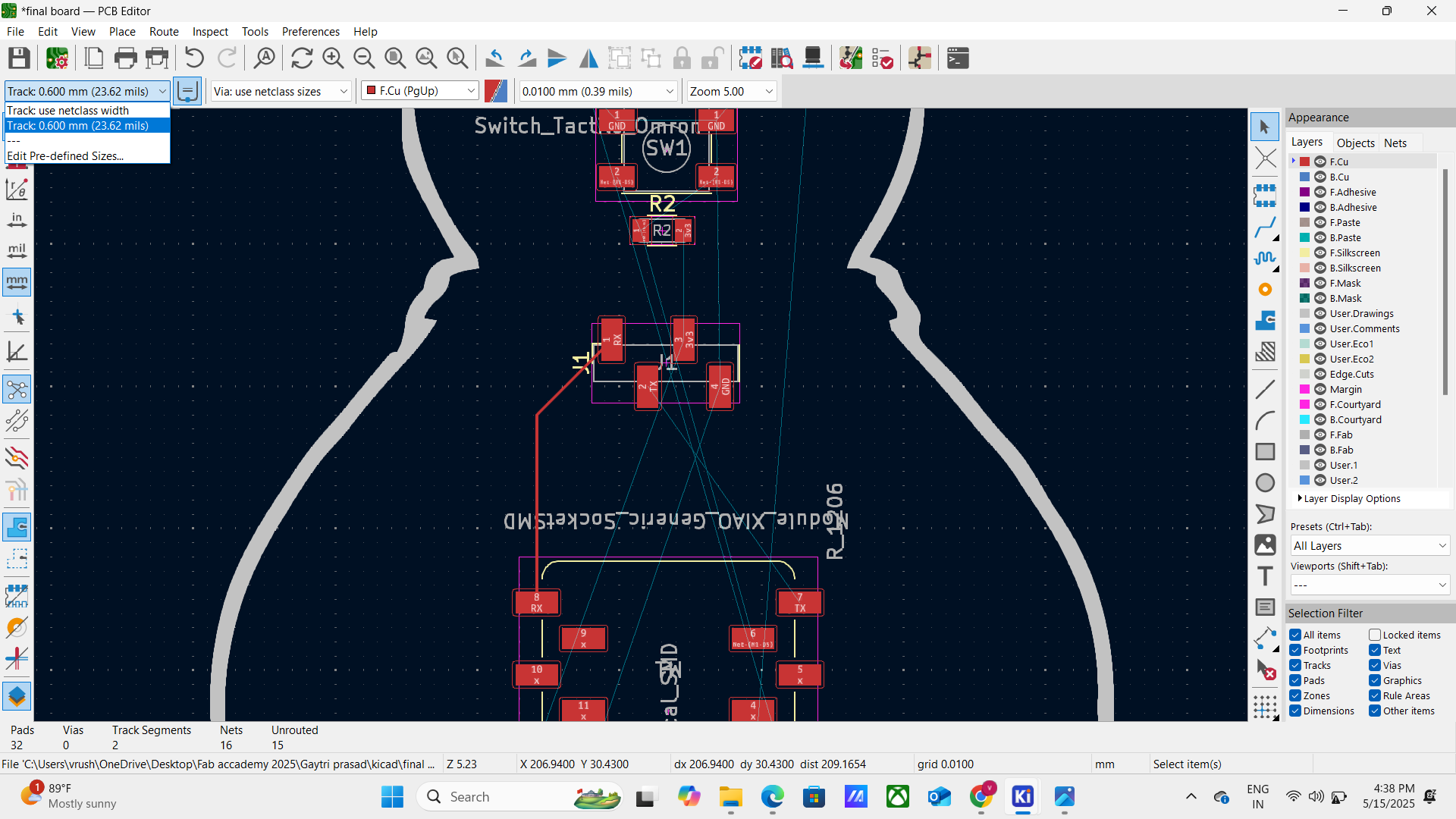
• Draw the board outline
• Route tracks manually (or use autorouter, if available)
- Design Rule Check (DRC): Run DRC to detect spacing, clearance, and overlap violations.
- Add Silkscreen, Text, and Logos: Place reference labels, orientation marks, and optional branding or logos.
- Generate Gerber Files: Use the “Plot” tool to export Gerber and drill files for PCB fabrication.
- Design Rule Check (DRC) completed with no errors
- Minimum trace width and clearance set according to milling tool size (1/64” bit)
- Traces and pads are clearly visible and properly separated
- No overlapping or short circuits detected
- Toolpath generated and verified using Mods
- Milling preview confirms proper isolation and cut paths
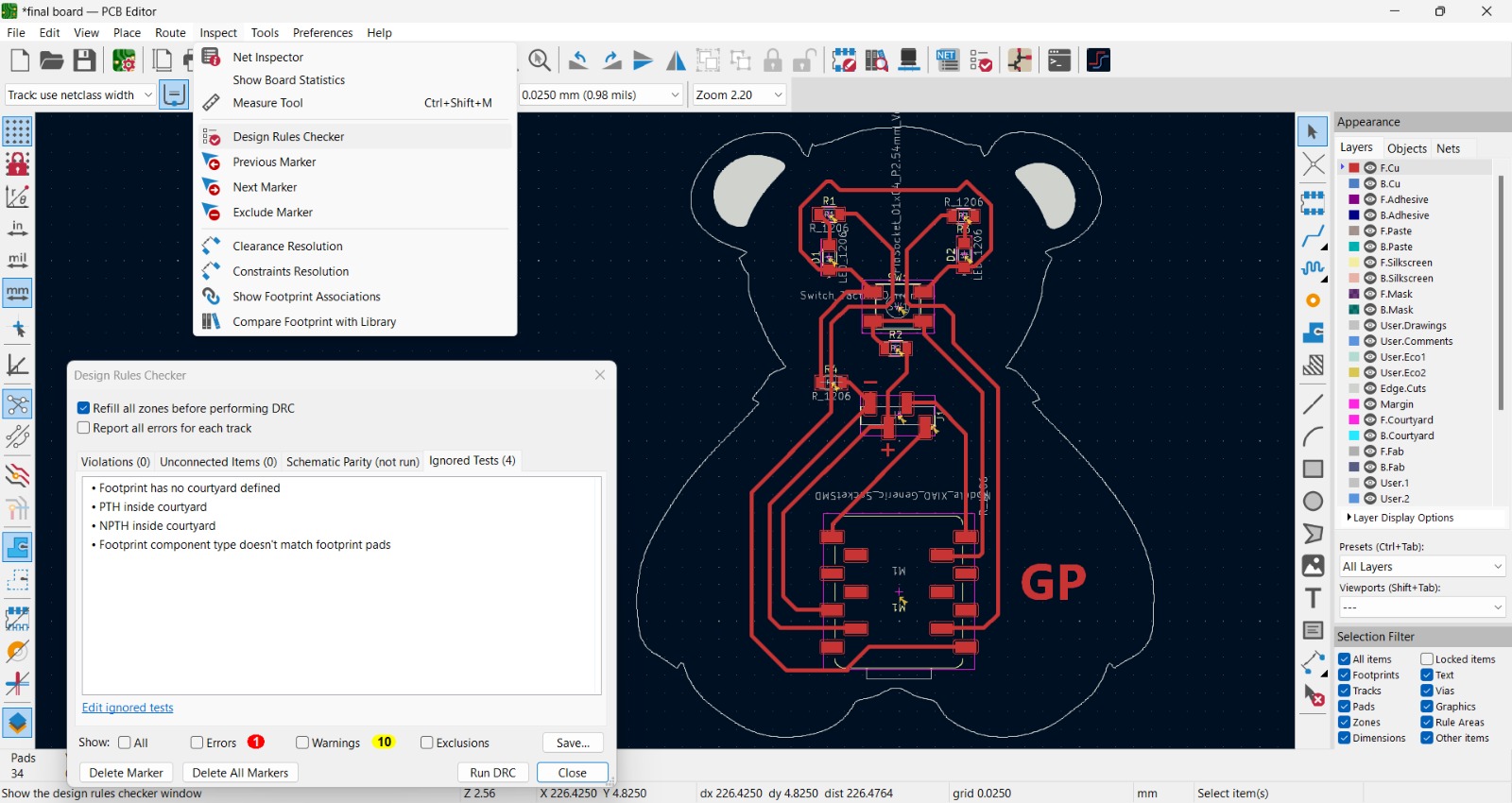
Final Fabrication Check
After completing the design, I verified that the PCB can be fabricated using the Fab Lab milling process:
Result:
Checked that the board can be fabricated successfully
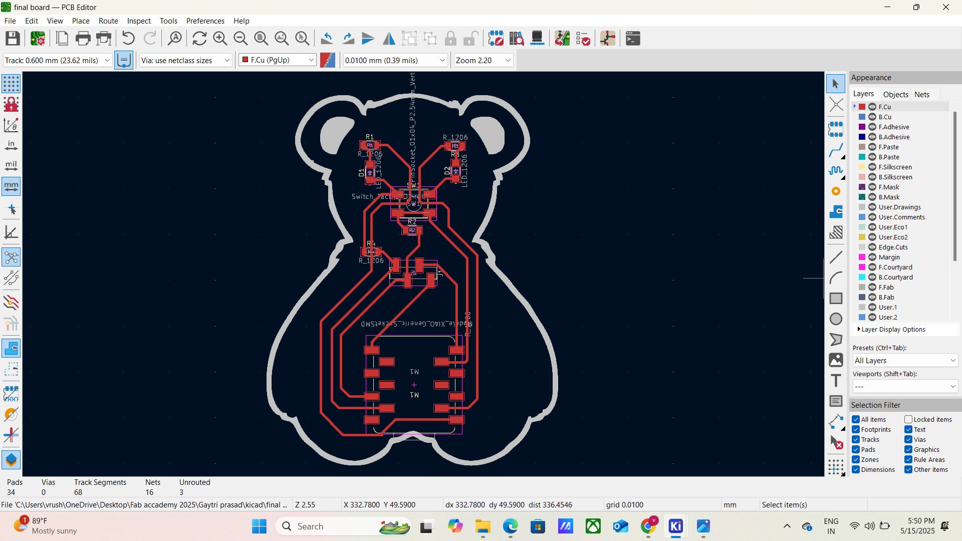
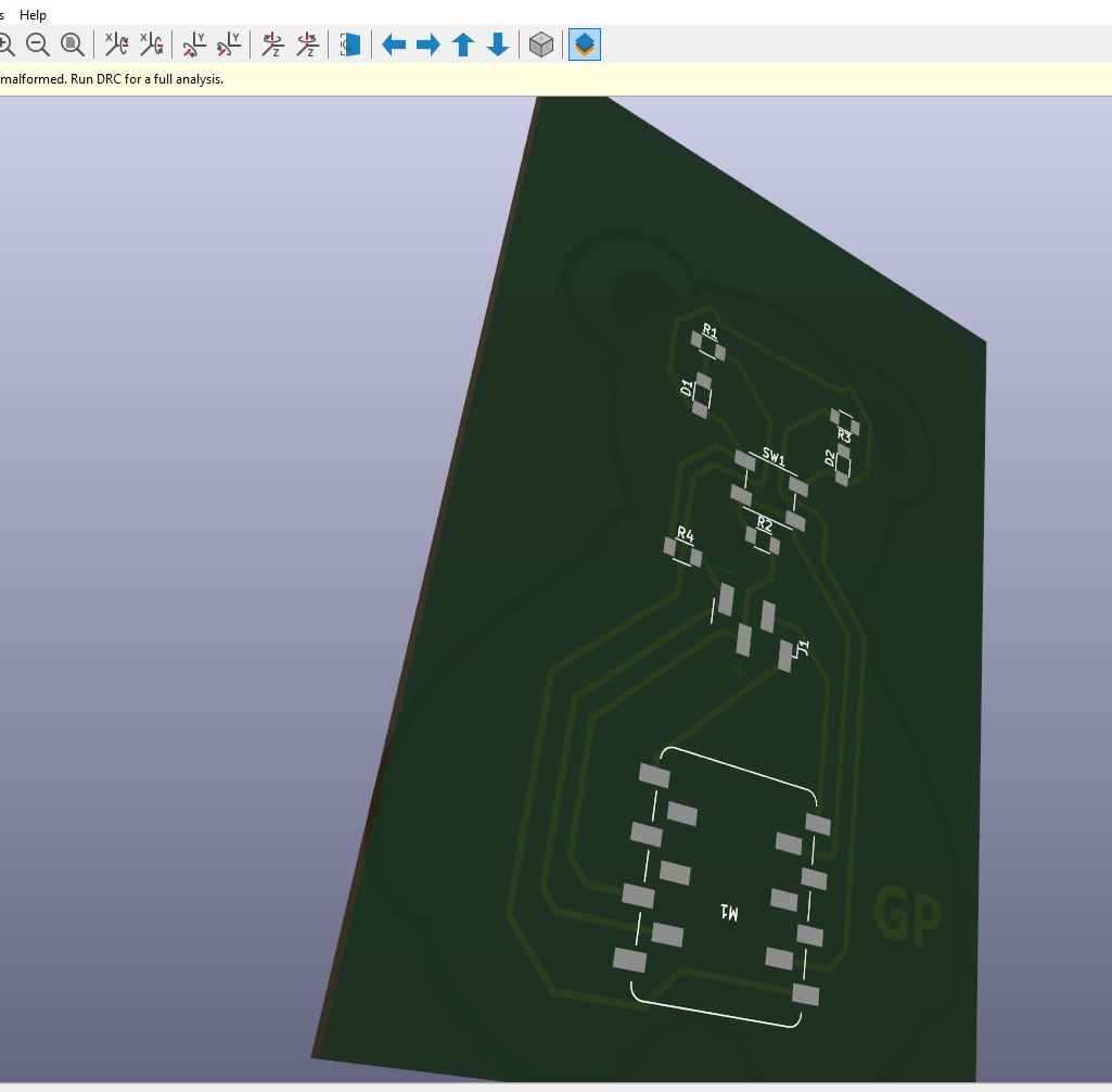
3d view of my board

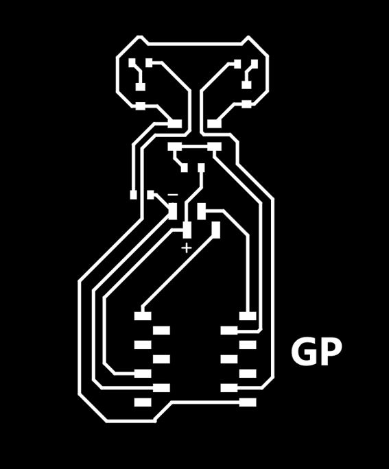
File svg

File Manufacturing Review .
The development board design demonstrates a good understanding of the electronic design workflow using KiCad. The schematic, PCB layout, ERC/DRC verification, and fabrication readiness checks are documented. To strengthen the documentation, include a detailed explanation of the circuit design, component selection rationale and PCB layout . Additional evidence showing manufacturability, such as trace width measurements and milling constraint verification, would further improve the review. Overall, the board appears ready for fabrication and aligns well with the assignment requirements.