KiCAD (Install & Fab Inventory Library & Schematic & PCB )
Hero Shot
Summary
This week, I focused on electronic design by creating a custom PCB using KiCad. I began by installing KiCad and setting it up with the Fab Academy 2025 component library, then designed a board based on the RP2040 microcontroller with integrated LEDs. The entire process is outlined step by step below.
I dove deeper into schematic design and component symbol management in KiCad, ensuring the Fab Academy inventory library was properly integrated. I explored the available components and designed a basic circuit featuring three push buttons, capacitors, resistors, and an LED, all connected to the RP2040. Once the schematic was complete, I verified the footprint accuracy for each component.
With the schematic finalized, I moved on to the PCB layout. In KiCad’s PCB Editor, I imported the schematic, arranged the components logically, and routed the necessary connections. This step ensured that the final PCB layout was both functional and ready for fabrication.
Work Process Detail
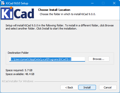
1. Installing KiCad
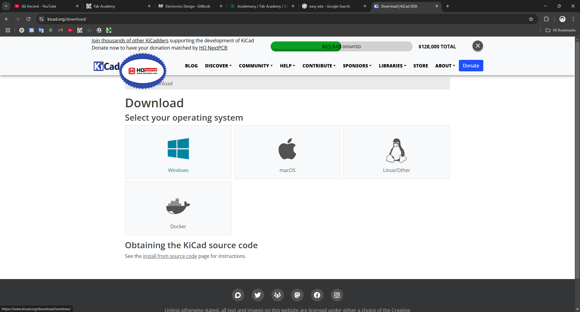
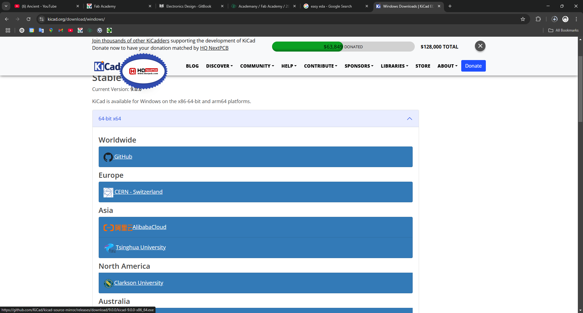
https://downloads.kicad.org/kicad/windows/explore/stable
- I visited the official KiCad EDA website and downloaded the Windows version.
- After downloading, I followed the GitHub installation link to ensure I installed the latest version.
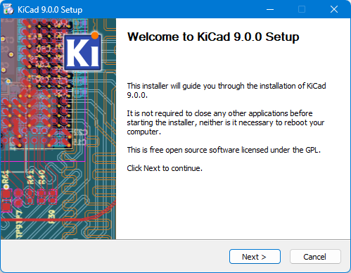
- I proceeded with the installation wizard, clicking Next until the process was complete.
- Once installed, I launched KiCad to confirm that it was working correctly.

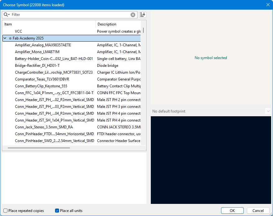
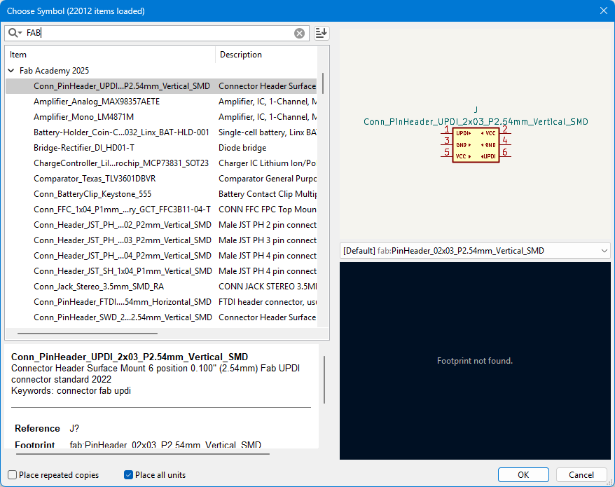
2. Adding the Fab Academy Inventory Library
- To make my experience smoother, I added the Fab Academy component library to KiCad.
- I followed the step-by-step instructions from a GitHub repository.
https://gitlab.fabcloud.org/pub/libraries/electronics/kicad
- Clone or download this repository. You may rename the directory to
fab.
- Store it in a safe place such as
~/kicad/librariesorC:/kicad/libraries.
- Run KiCad or open a KiCad
.profile.
- Go to "Preferences / Manage Symbol Libraries" and add
fab.kicad_symas symbol library.
- Go to "Preferences / Manage Footprint Libraries" and add
fab.prettyas footprint library.
- Go to "Preferences / Configure Paths" and add new environment variable "FAB" that points to location of the fab library on your drive, e.g.
~/kicad/libraries/fab. This is needed for the 3D models to load correctly.
- Clone or download this repository. You may rename the directory to
- I imported the schematic symbols and footprint libraries to ensure that all necessary components were available for PCB design.
- After installation, I verified that the library loaded correctly inside KiCad.
3. Creating A Noob PCB Design
- I started a new project in KiCad and created a schematic for my PCB.
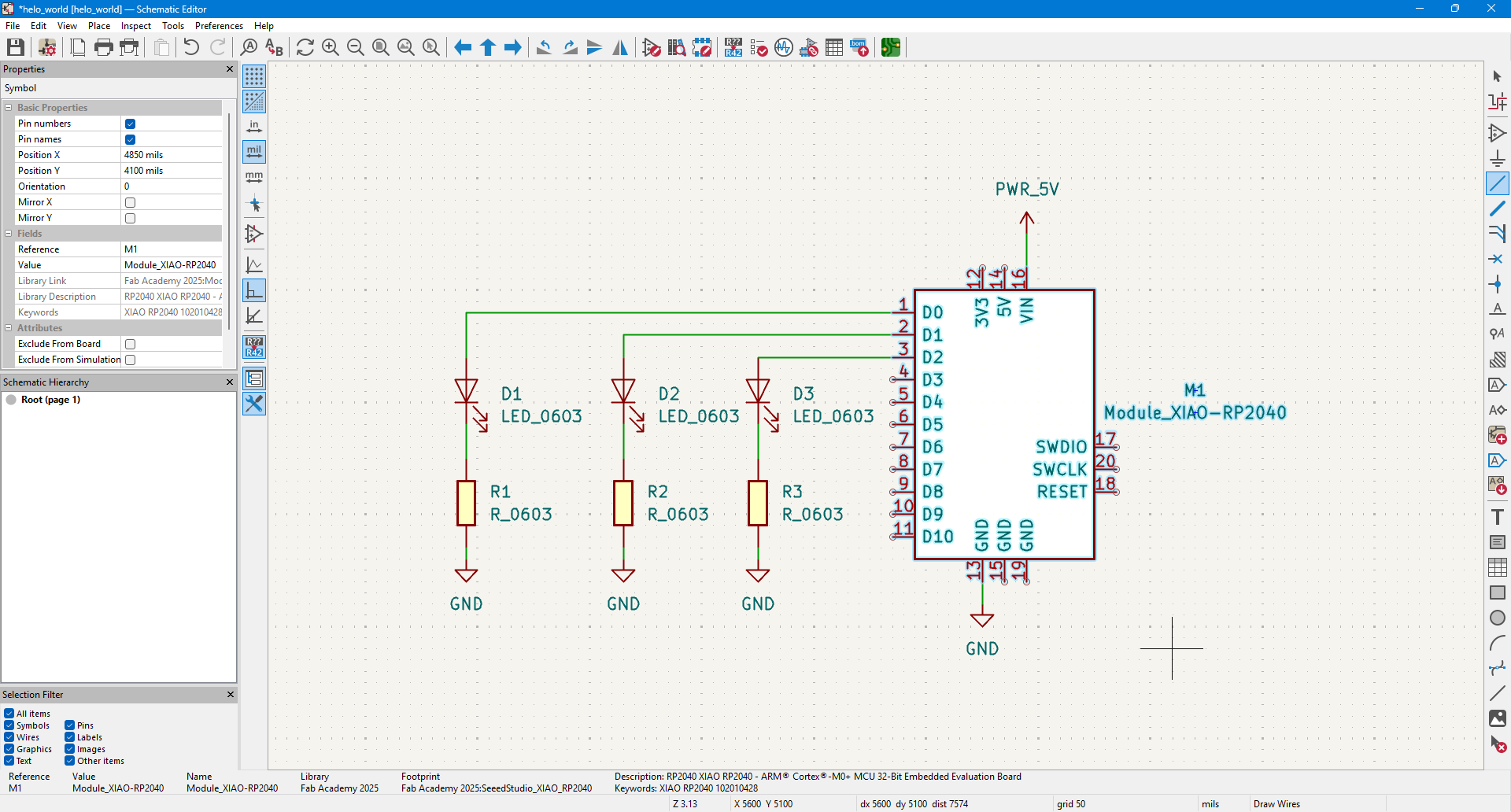
- The design included the RP2040 microcontroller and LEDs to test basic circuit functionalities.
- I placed and wired components in the schematic editor before proceeding to PCB layout.
- Once the schematic was complete, I assigned footprints and moved on to designing the board layout.
Main Board (Schematic + Symbol):
1. Setting Up the Fab Academy Library
- I ensured that the Fab Academy 2025 inventory library was properly installed and active in KiCad.
- I browsed through the available components in the inventory to understand which parts were locally available for my design.
2. Selecting and Placing Components
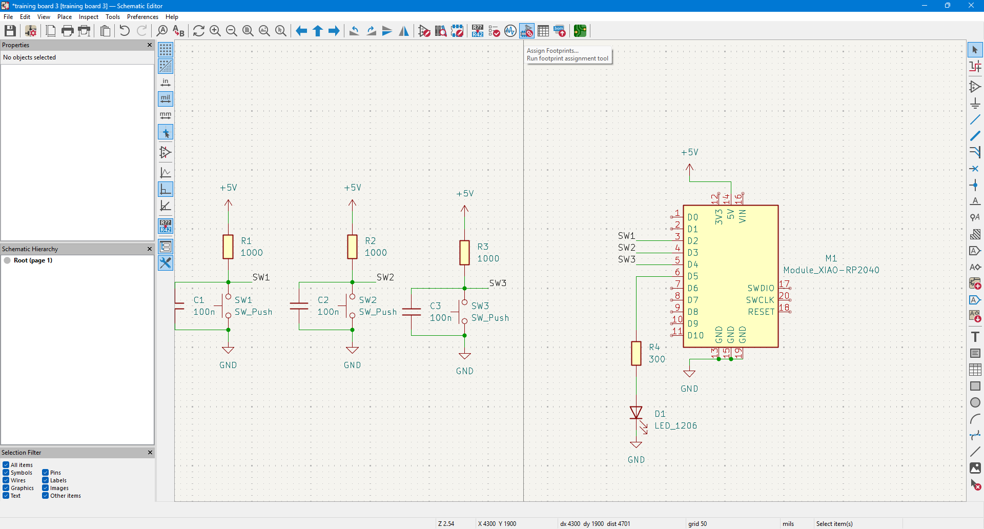
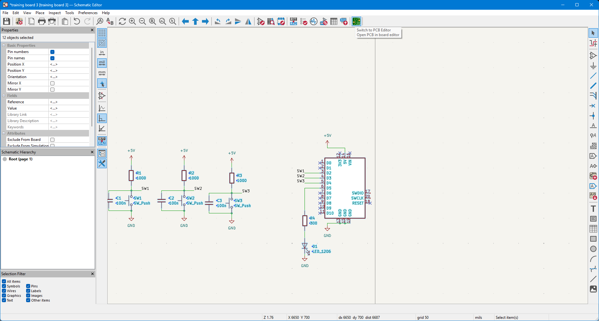
- After reviewing the inventory, I decided to create a simple example circuit using:
- Three push buttons as inputs.
- Capacitors and resistors to stabilize the circuit.
- RP2040 microcontroller as the main control unit.
- GND
- VCC


- I carefully placed the components in KiCad's schematic editor, ensuring proper connections and logical flow.


- Then i used ERC⇒ Electrical Rules Checker to make sure everything is right, and refixed the problem.


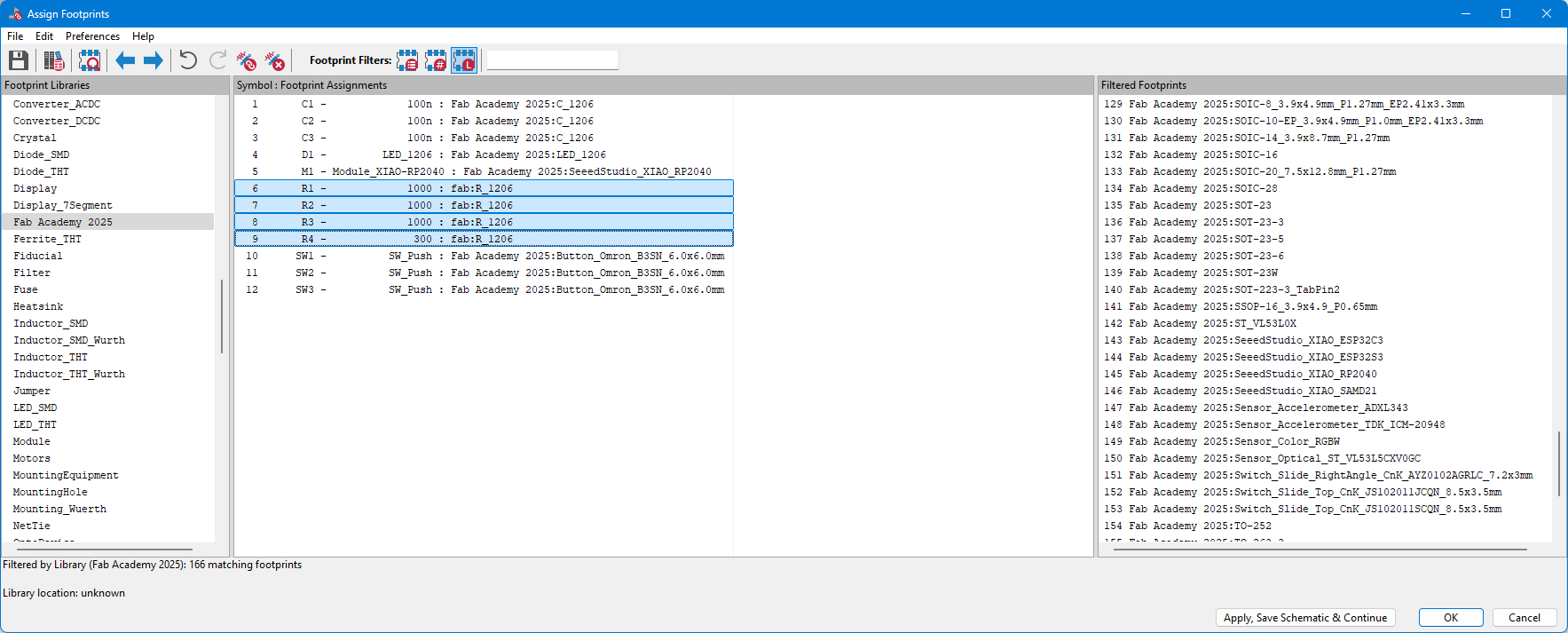
3. Assigning and Aligning Footprints
- After finalizing the schematic, I proceeded to assign the correct footprints for each component.
- I verified that the footprint dimensions matched the physical components to avoid misalignment during PCB fabrication.
- Ensured that pad sizes, hole placements, and spacing were correct for soldering.


Main Board(PCB + Footprint)
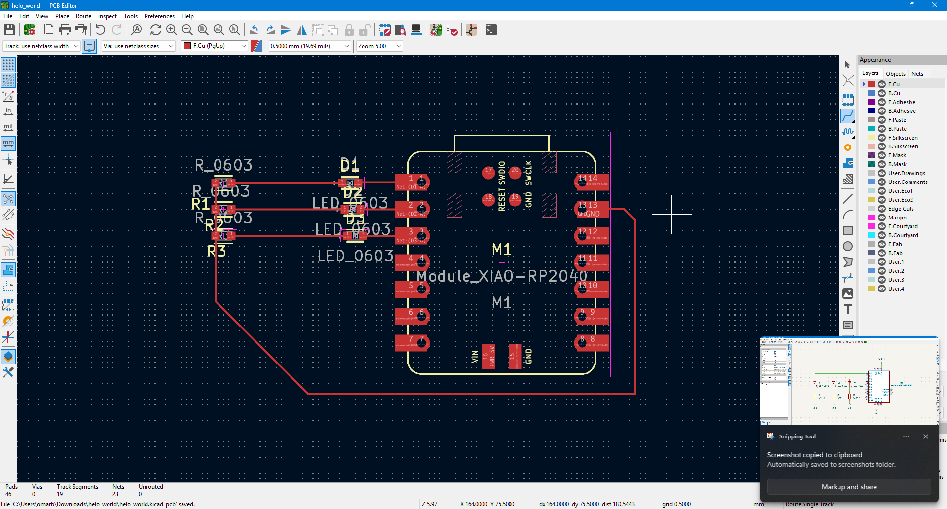
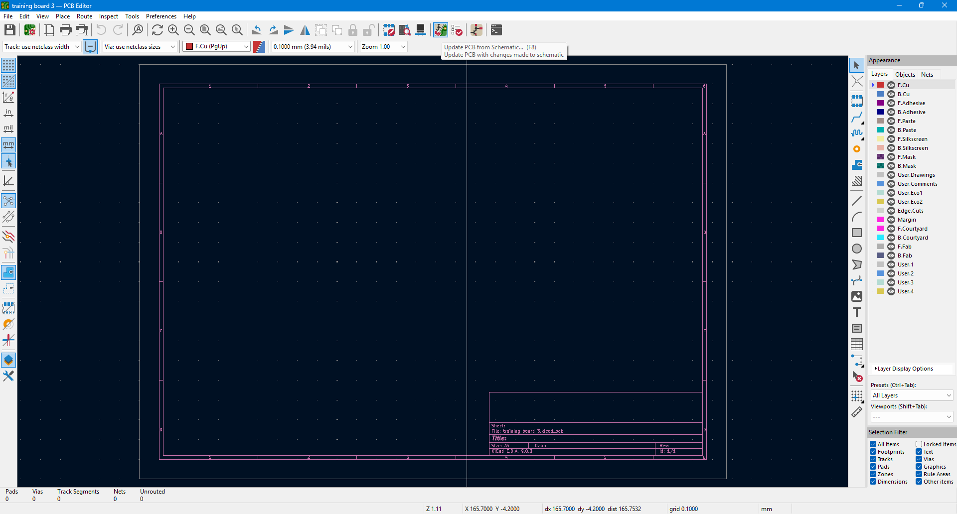
- After confirming that all schematic connections were correct, I went to the "Update PCB from Schematic" section in KiCad.
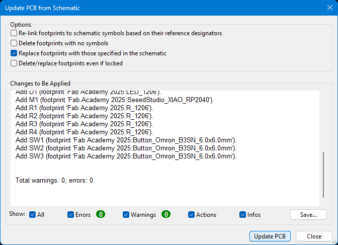
- I clicked “Update PCB from Schematic” to import all component footprints into the layout.
- I verified that there were no errors during the import and placed all components in the center of the workspace.

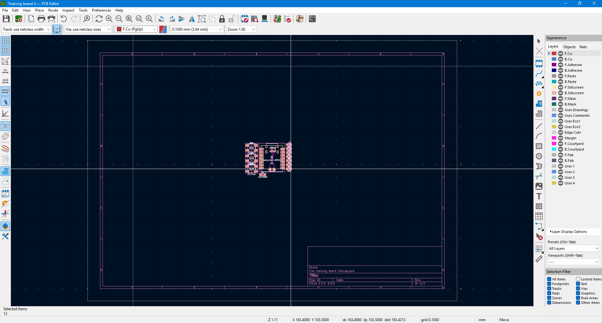
- Using the Select Tool, I arranged and rotated the components to fit the final board layout.
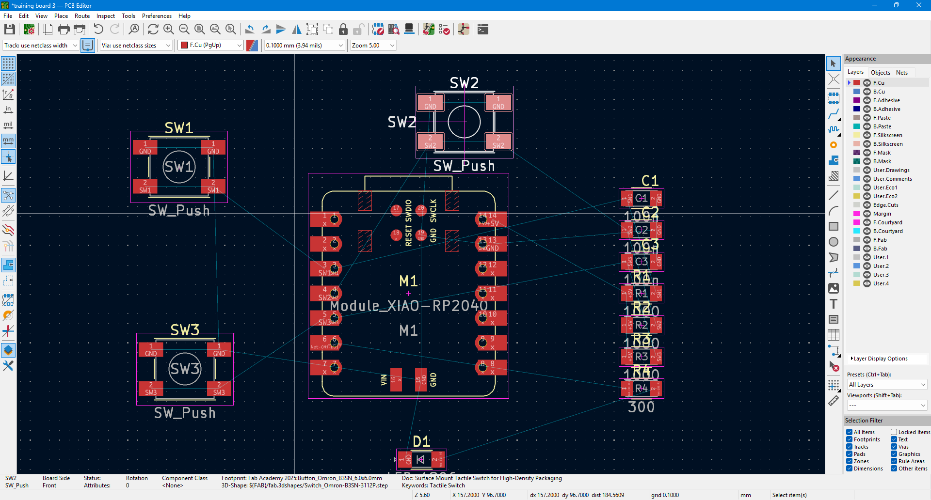
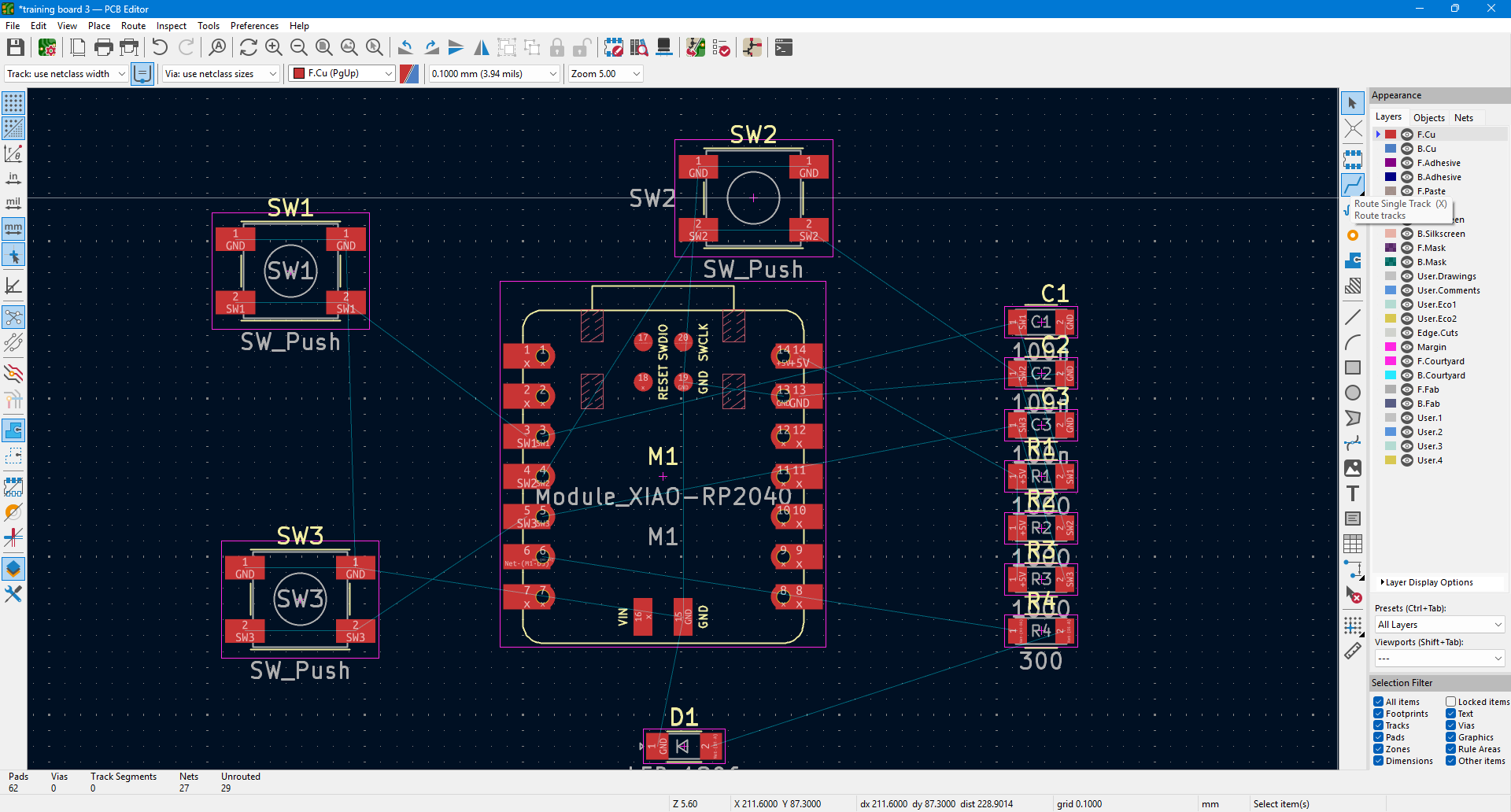
- I used the Route Tracks tool to draw traces connecting all components—buttons, capacitors, and others.


- Once routing was complete, I switched to the Edge.Cuts layer and drew a rectangle around the circuit to define the board’s boundary.
- Then, I selected “Add Filled Zones”, chose the top copper layer (red), and drew a filled rectangle to define the ground plane.

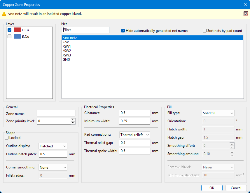


- Pressing ‘B’ on the keyboard generated the ground fill across all relevant connections.
- Before moving on to show you the 3D preview of the PCB, I'm going to check the DRC to ensure everything is functioning correctly. If I find any errors, I'll work on fixing them to make sure the design is clean. For this project, I’ll be using a manual wire to bridge the pins that don’t have proper traces, since this is purely for educational and learning purposes.


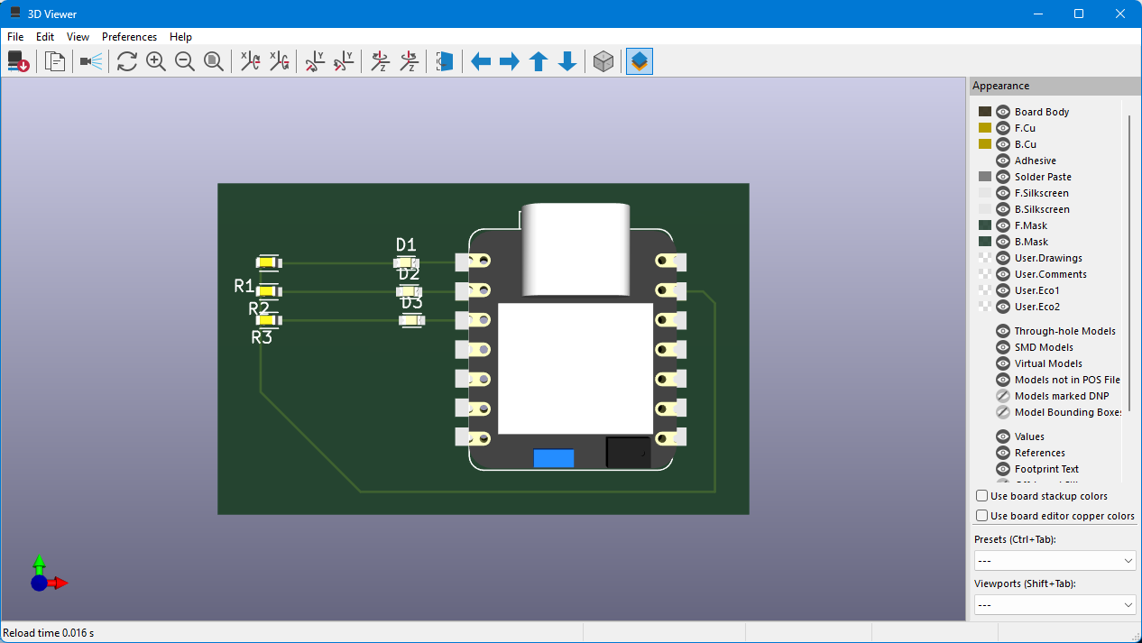
- I reviewed the design using the 3D Viewer to ensure the board looked correct.

- Finally, I prepared the design for fabrication by going to File > Plot, selecting the Top Layer and Edge.Cuts, setting the output format to SVG, and exporting the file to use in the fabrication process.


Learning Outcome
🔹 Getting Started with KiCad
- Installed KiCad and set it up with the Fab Academy library.
- Designed a simple PCB schematic with the RP2040 and LEDs.
- Routed the PCB to connect everything correctly.
- Ran a Design Rule Check (DRC) to make sure there were no errors.
🔹 Working with Components
- Made sure the Fab Academy 2025 library was installed.
- Looked through the parts and chose the right ones.
- Built a basic circuit using buttons, resistors, and capacitors with the RP2040.
- Added the correct footprints for each component.
- Checked the sizes and spacing to avoid mistakes in manufacturing.
🔹 From Schematic to PCB
- Switched from schematic to PCB view in KiCad.
- Synced the schematic with the PCB layout.
- Fixed any errors or warnings.
- Placed parts neatly and routed the wires.
- Used good layout practices for a clean design.