Etching + UV printer
Summary
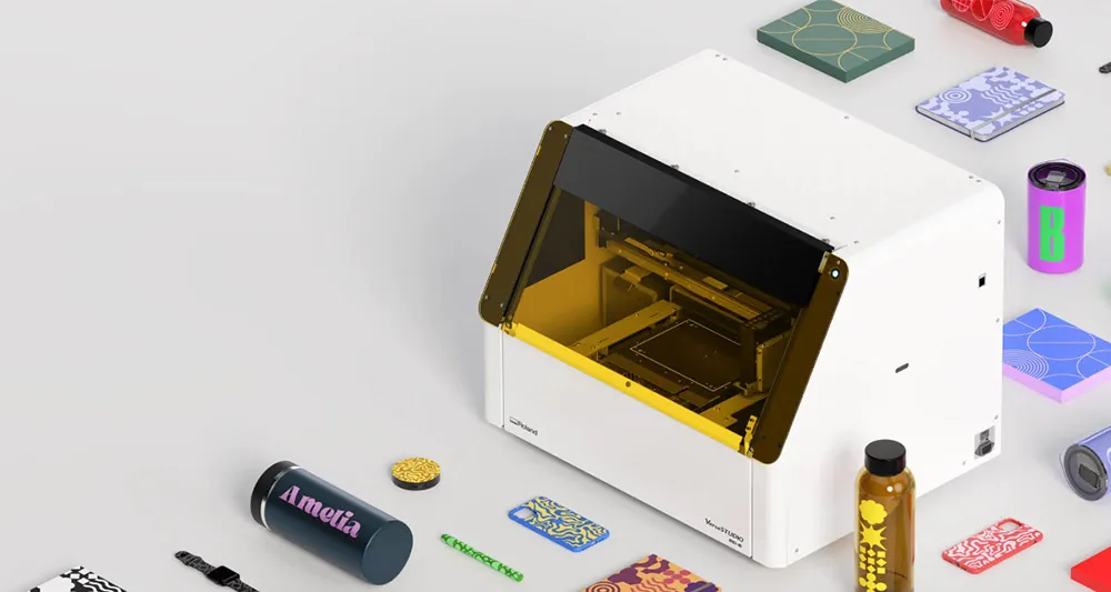
This week, I explored a new PCB fabrication method using the VersaStudio BD-8, a direct-to-surface printer that allows printing on various materials, including PCB copper boards. Instead of milling, I used etching with ferric chloride to create the circuit. This method proved to be more accurate than the traditional milling process. Below is the step-by-step process I followed.
Work Process Detail
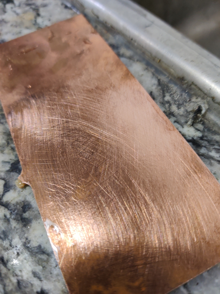
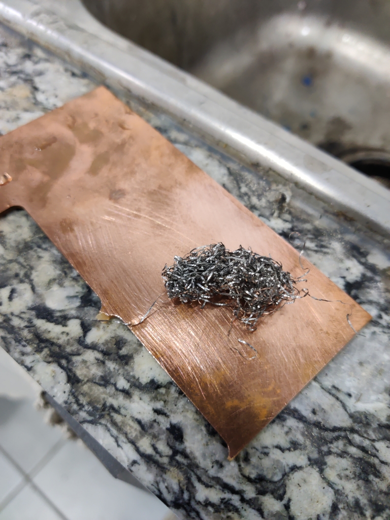
1. Preparing the PCB Copper Board
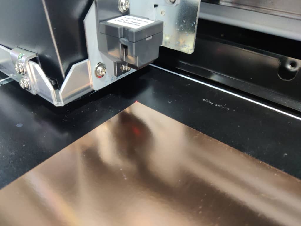
- Cleaned the copper surface to remove any oxidation or rust.
- Ensured the board was completely dry and smooth for better print adhesion.
📷 In this photo: The copper board after cleaning, ready for printing.
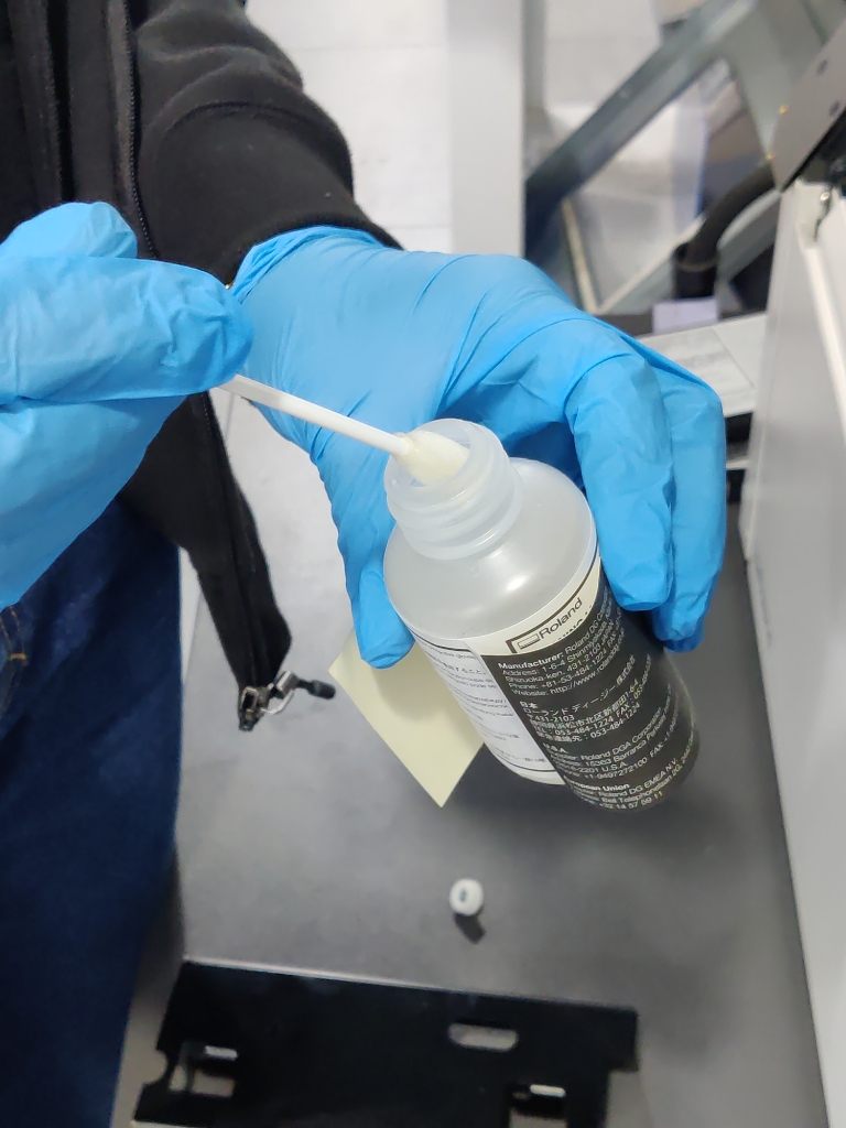
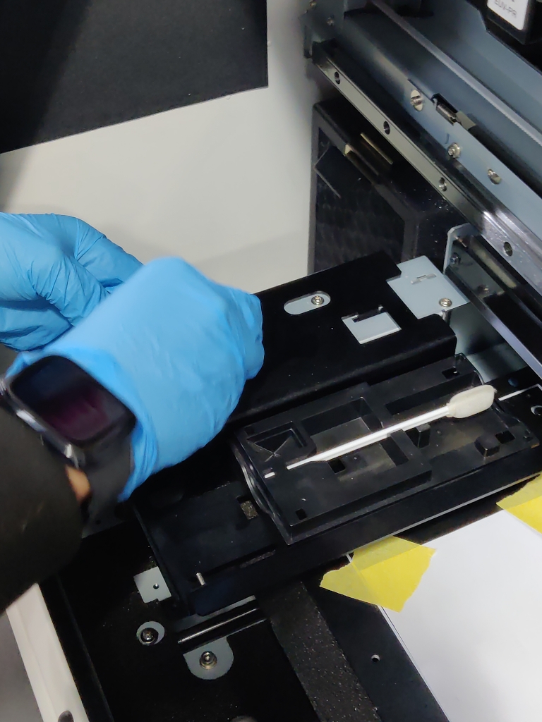
2. Cleaning the Printer Head & Preparing for Printing
- Performed printer head cleaning to avoid ink clogs.
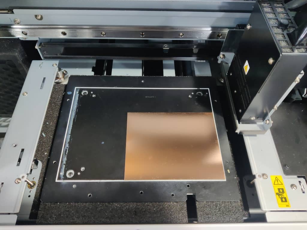
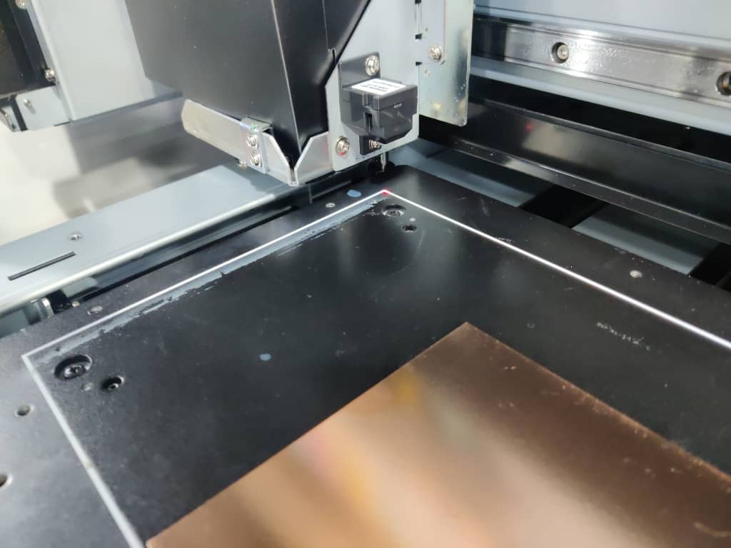
- Loaded the PCB copper board into the VersaStudio BD-8.
📷 In this photo: The VersaStudio BD-8 printer setup for PCB printing.
3. Printing the Circuit Design on the PCB Surface
- Uploaded the PCB trace image to the printer software.
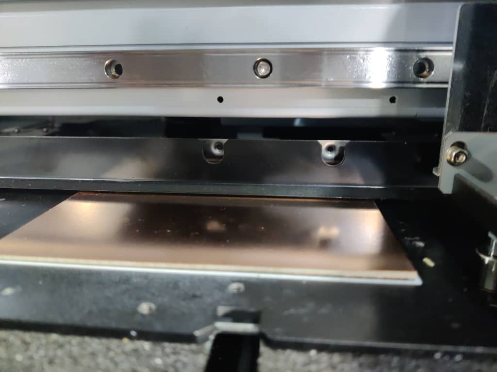
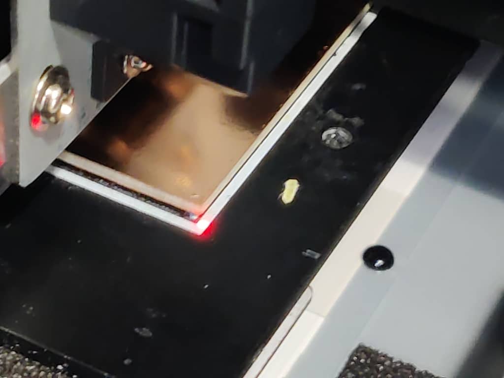
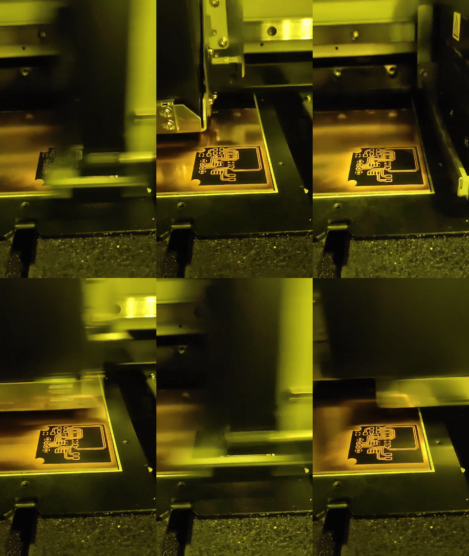
- Printed the circuit layout directly onto the copper board.
- Allowed the print to dry completely before proceeding.
📷 In this photo: The PCB images printed on the copper surface.
.png)
.png)
.png)
.png)
.png)
.png)
.png)
.png)
.png)
.png)
.png)
.png)
.png)
.png)
.png)
.png)
.png)
.png)
4. Cutting the Board to the Exact Size
- Used a saw to cut the board to the exact dimensions needed for the project.
📷 In this photo: The PCB being cut to size with precise measurements.
.jpg)
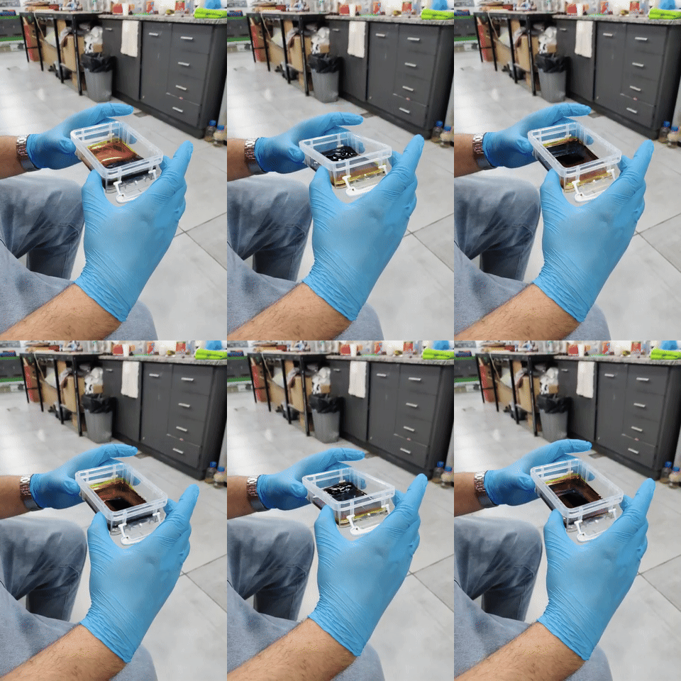
5. Etching the PCB with Ferric Chloride
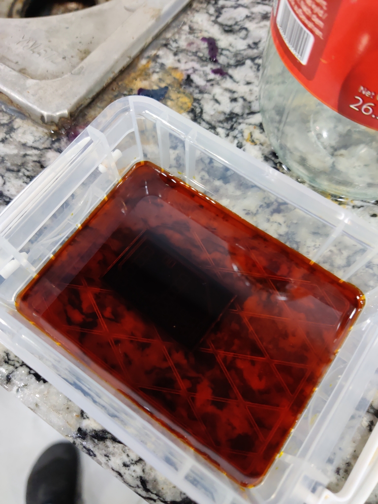
- Submerged the printed PCB into a ferric chloride solution to dissolve unwanted copper.
- Used proper safety measures (gloves, ventilation, protective eyewear).
- Monitored the etching process until the circuit traces were fully formed.
📷 In this photo: The PCB submerged in ferric chloride during etching.
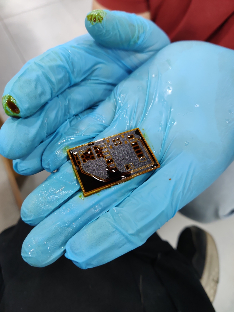
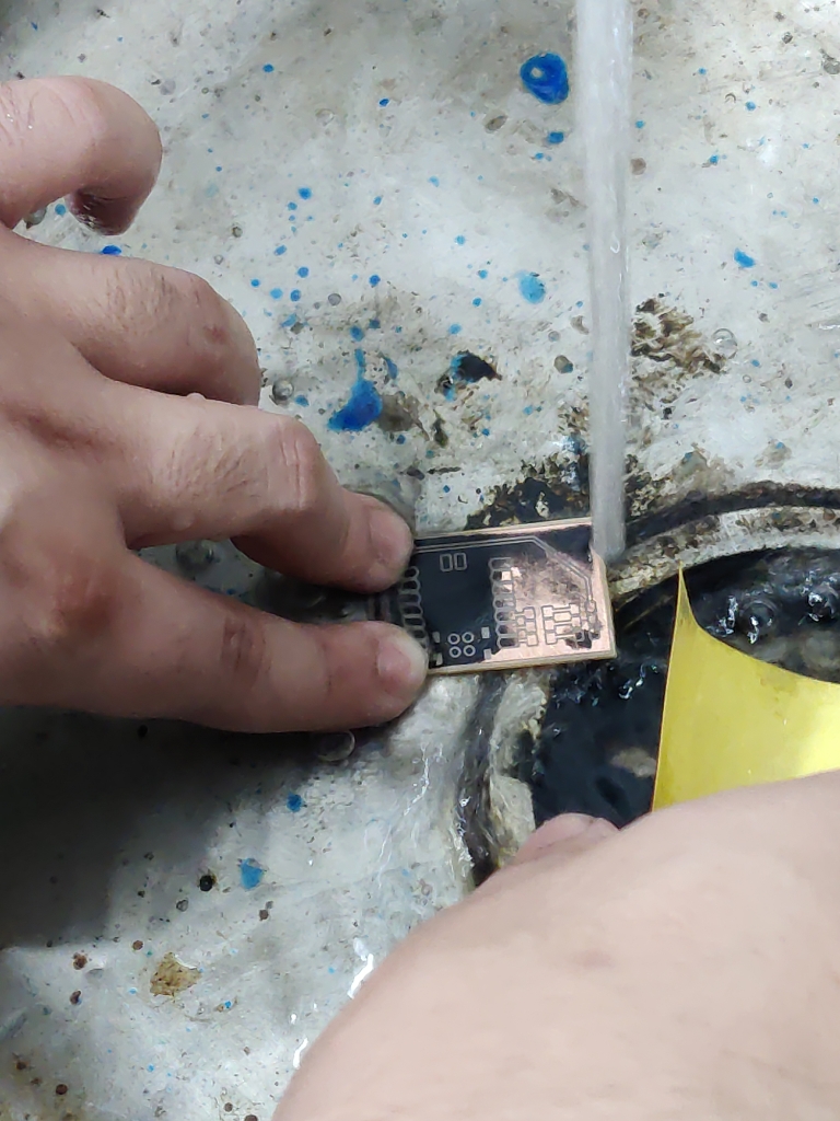
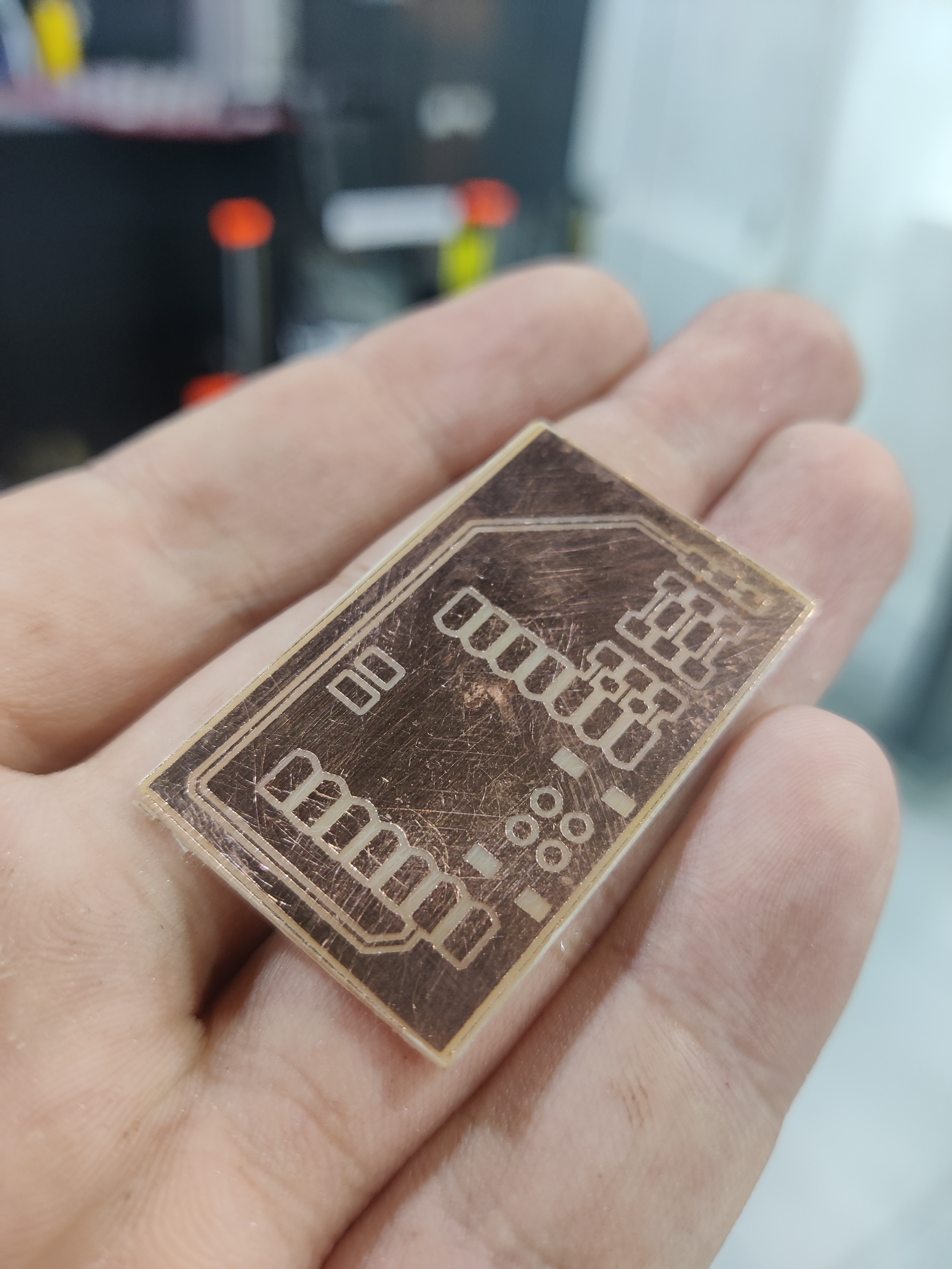
6. Cleaning and Finalizing the PCB
- Used sandpaper to remove any remaining ink and smoothen the board.
- Ensured that all traces were fully etched and clearly visible.
📷 In this photo: The PCB after etching and cleaning, ready for soldering.
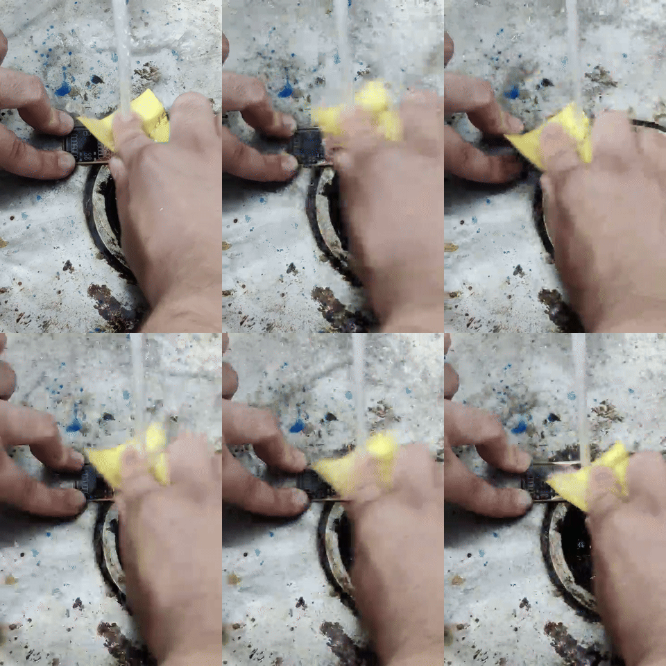
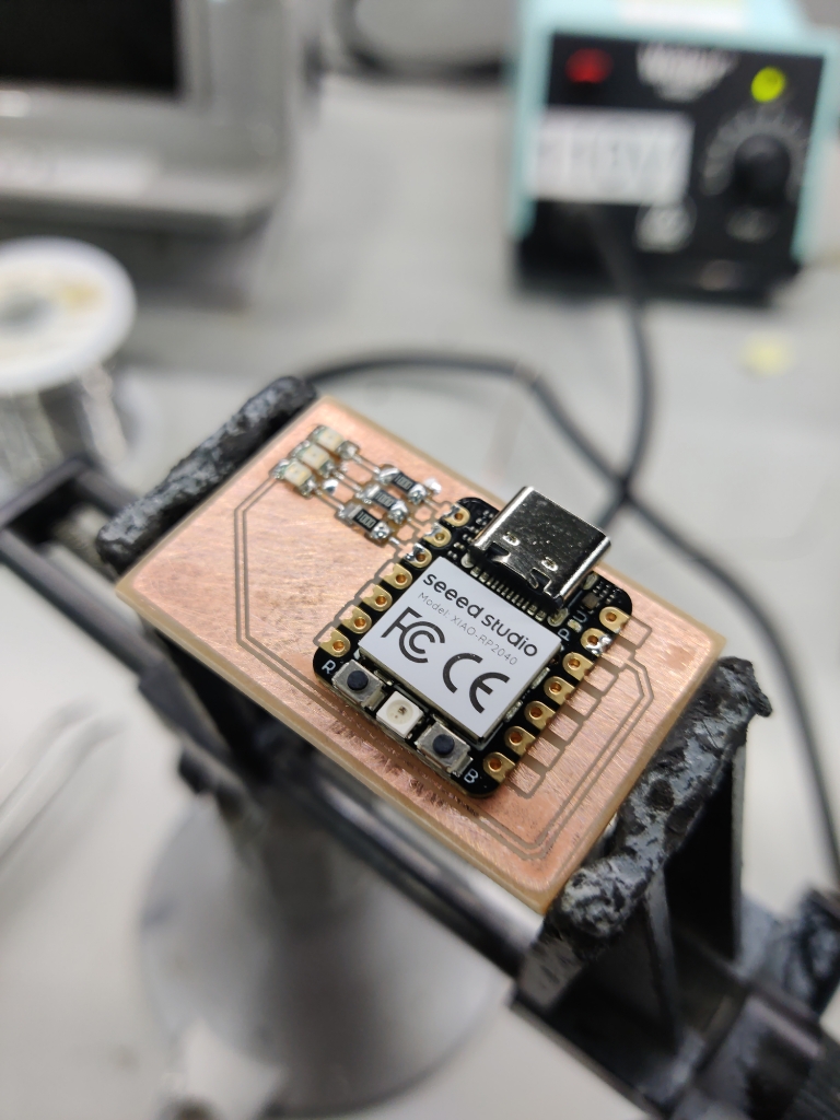
7. Soldering Components and Microcontroller
- Placed and soldered the resistors, capacitors, microcontroller, and other components.
- Ensured proper alignment and clean solder joints.
📷 In this photo: The PCB with all components soldered in place.
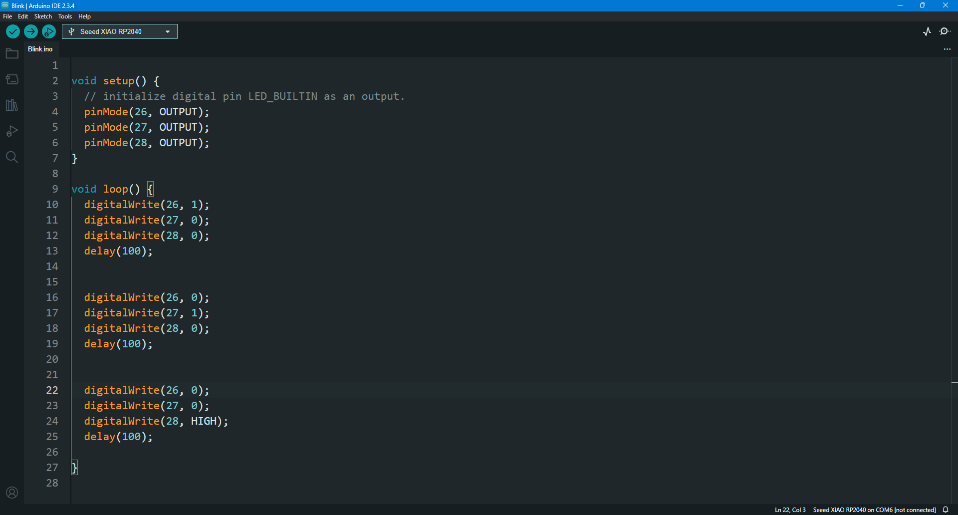
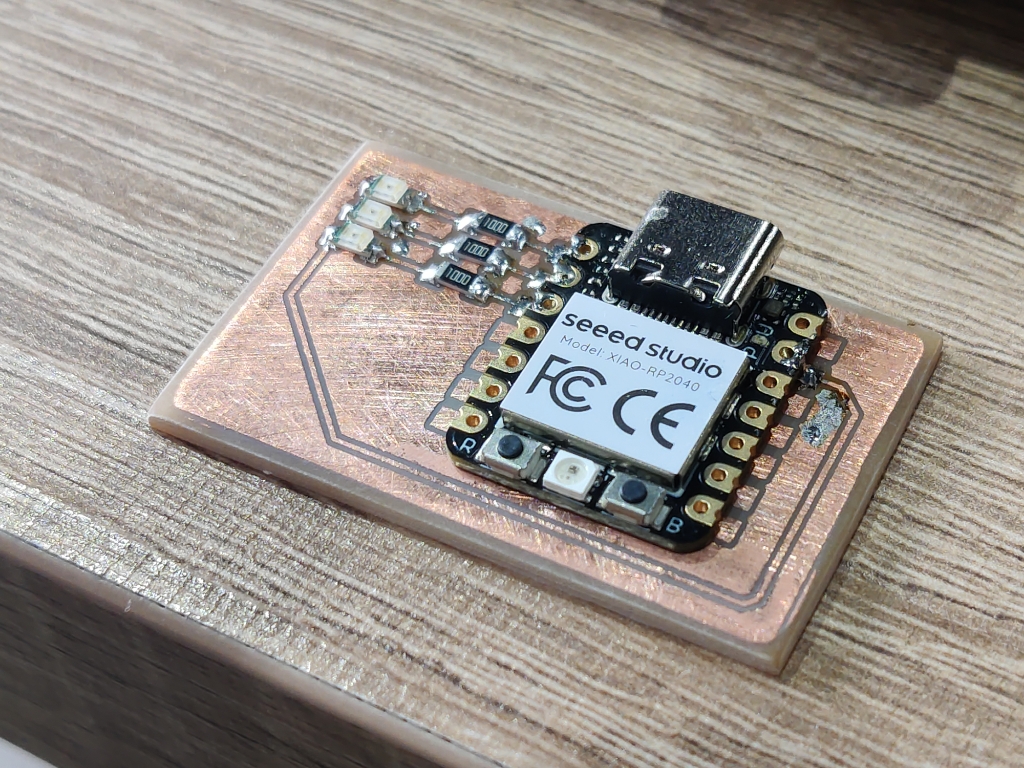
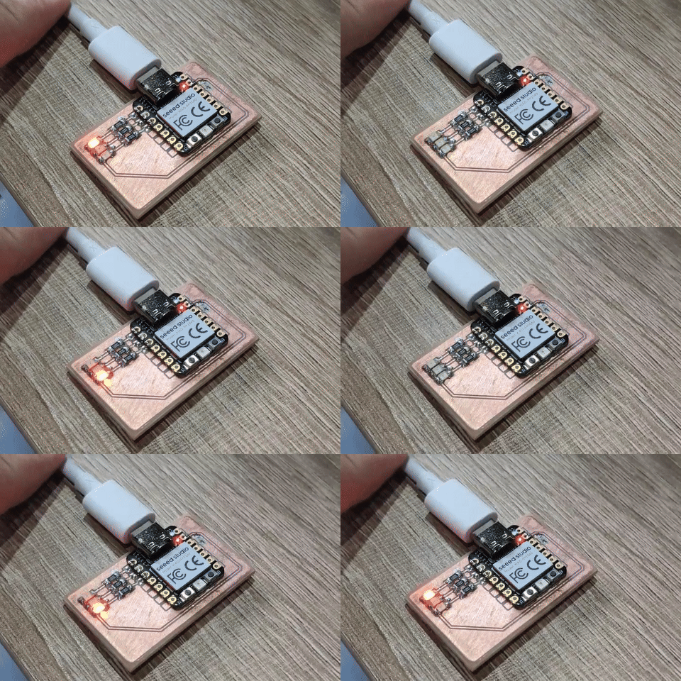
8. Uploading Code & Testing the PCB
- Connected the microcontroller to a computer and uploaded the firmware.
- Tested the PCB for continuity and proper functionality.
📷 In this photo: The final PCB connected for testing.
Learning Outcome
1️⃣ Discovered a new PCB fabrication method using direct-to-surface printing and etching.
2️⃣ Understood how to prepare and clean the PCB surface for better print adhesion.
3️⃣ Learned how to handle ferric chloride etching with proper safety precautions.
4️⃣ Compared accuracy between milling and etching, finding that printing and etching were more precise.
5️⃣ Successfully soldered and tested the PCB, confirming that all traces were correctly formed.