This week is going to be an exciting deep dive into electronic production, where theory meets hands-on creation! You'll be immersing yourself in PCB fabrication, turning digital designs into tangible circuit boards. The thrill of selecting the right PCB materials adds an extra layer of precision, ensuring durability and efficiency.
Exploring board houses, where PCBs are professionally crafted, will broaden your understanding of the industry and manufacturing standards. Then comes the fun part—working with components like resistors and LEDs, shaping circuits that power real-world applications. Testing on breadboards allows for quick iterations and troubleshooting, a crucial step before moving to final assembly. And finally, the moment of transformation—assembling all the pieces onto your custom PCB, watching your circuit come to life!
I will use mods (a software tool) to create paths for a PCB milling machine, which cuts the circuit design onto the board. This will help me understand how to design and make my own circuits. serve as the uppermost component of the structure, ensuring a balanced and sturdy design.
Design using Kicad
In Week 6, we successfully designed the XIAO RP2040 using KiCad, bringing our vision to life with precise schematics and meticulous layout planning. Now, the excitement builds as we take this design to the next stage—transforming it into G-Code using MoDS projects! The anticipation of seeing the design materialize through fabrication is electrifying. From digital traces on the screen to a tangible circuit, every step in this journey deepens our understanding of PCB design, machining, and real-world application.
I met certain failure in design done in previous week at the time of printing, I have mentioned at the end of the page and I did certain modification in the design and final schematic layout is shown below
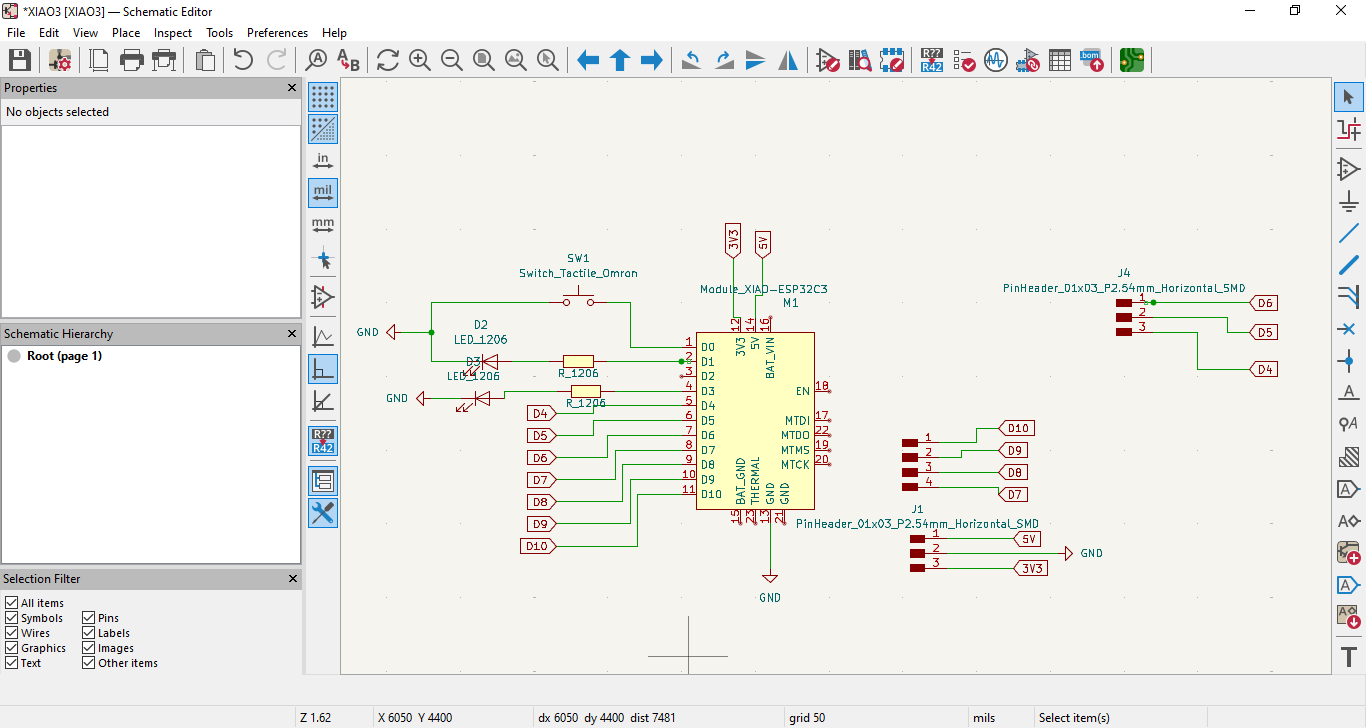
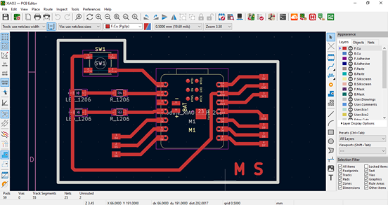
The PCB diagram showcases my design process, where I utilized the Xiao RP2040 board as the foundation. To enhance functionality, I incorporated a switch, an LED, and a connector, carefully integrating each component to create a cohesive circuit.
Then, I opened the PCB editor and used the "Route Track" command to make the necessary connections, ensuring that the PCB functions properly.
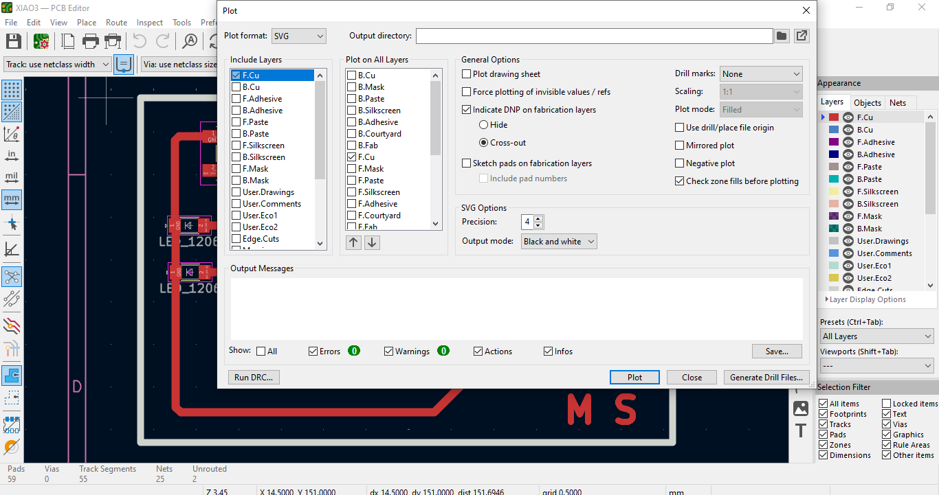
The next crucial step in the PCB fabrication process is saving the file in the appropriate format. Since PCB files are stored separately for traces and outline cuts, careful file management is essential. To save the trace file, navigate to the File menu and select Plot. In the Plot window, set SVG as the output format, ensuring a high-quality export.
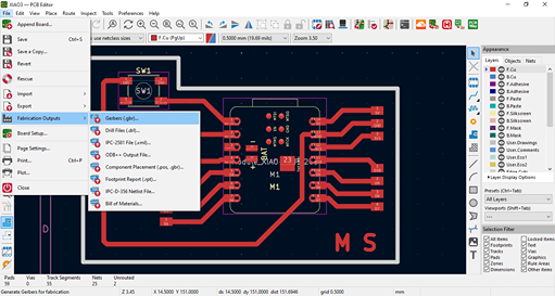
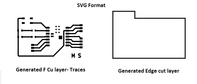
Choose F.Cu (the front copper layer) to capture the necessary trace details. Once completed, the system will confirm the save location of the file. Finally, clicking Save will securely store the trace file, preparing it for the next stage in the fabrication journey.
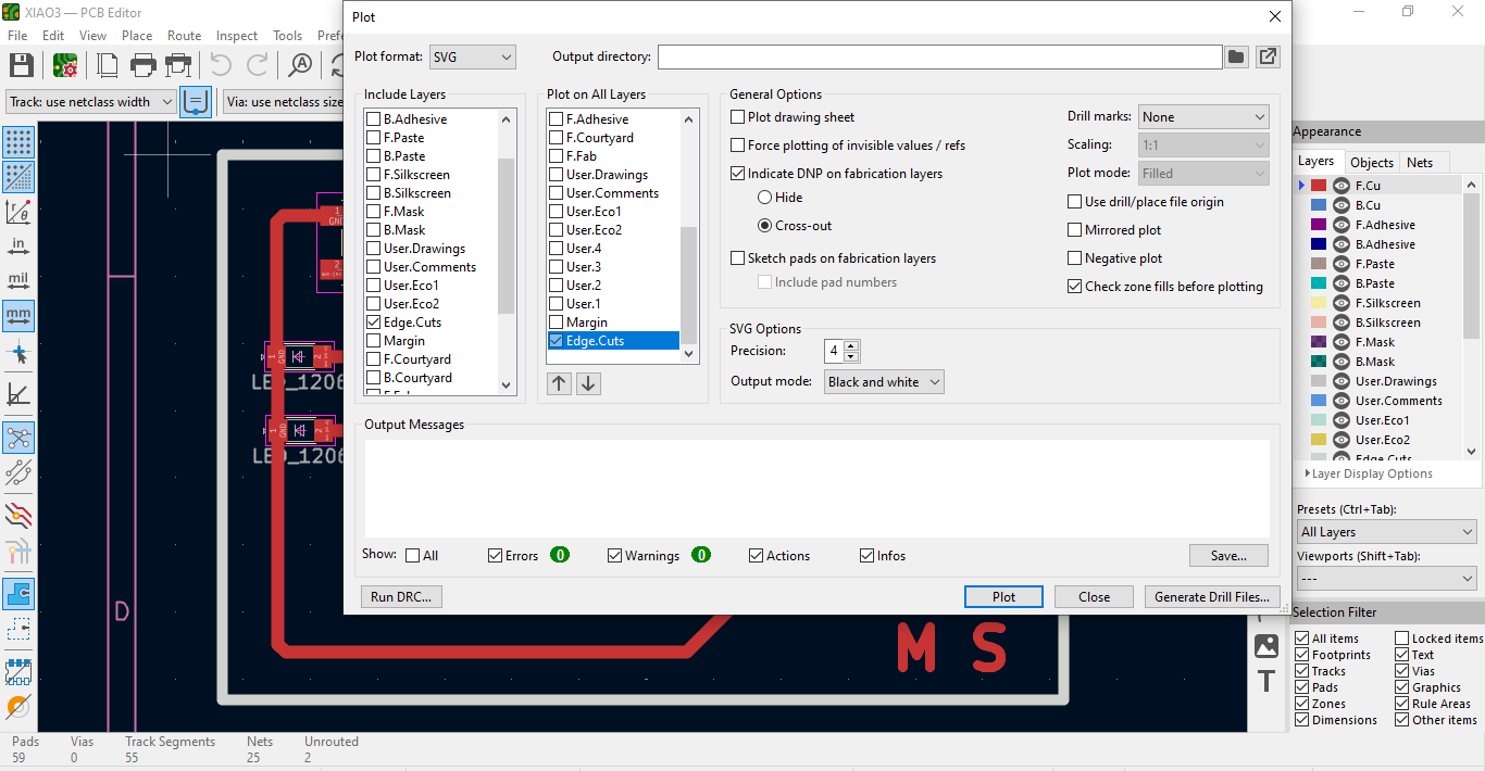
Same procedure is used to plot the edge cut layers in SVG format
SVG Format of both the files
Generate Toolpath for PCB Milling
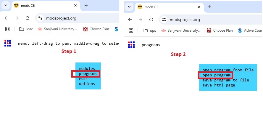
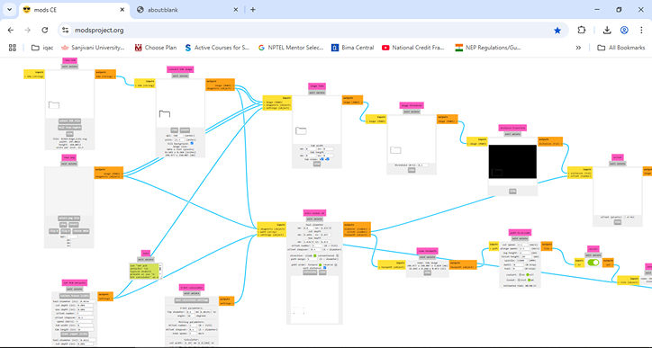
To generate the G-code for PCB milling, we used the online MODS interface developed by MIT's Center for Bits and Atoms (available at modsproject.org
1. Open the Mods Project website.
2. Once the website loads, the main window appears.
Followed the steps given as per the image for generating traces in .nc file
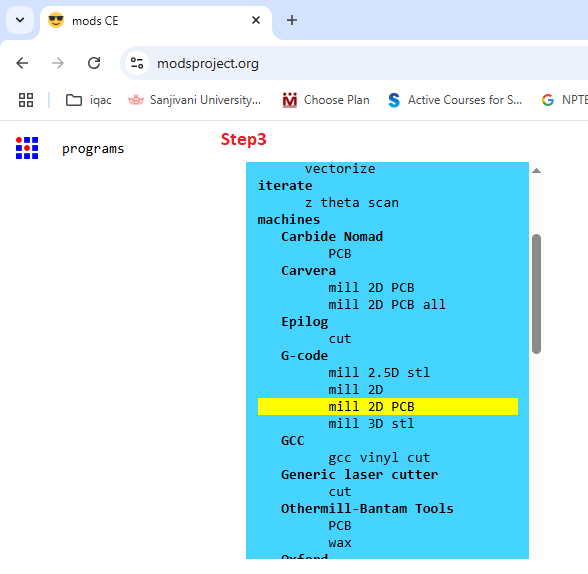
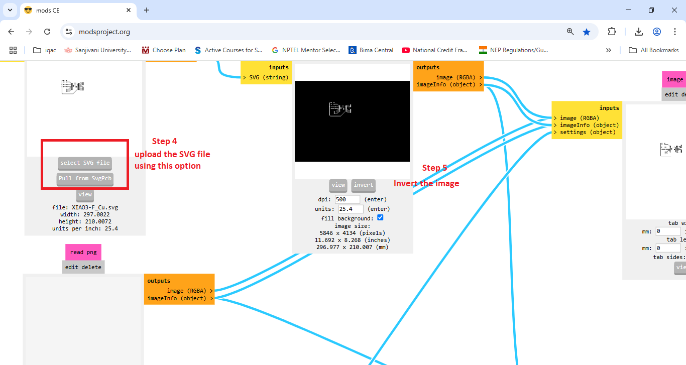
For generating .nc file the svg format of edge cut layer is uploaded and done as per the steps mentioned in the images
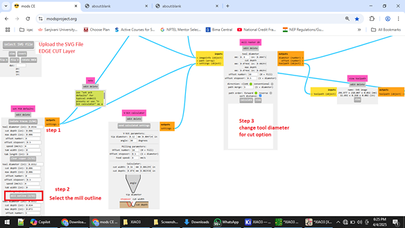
Entire process screen of MIT MODS for edge cut layer
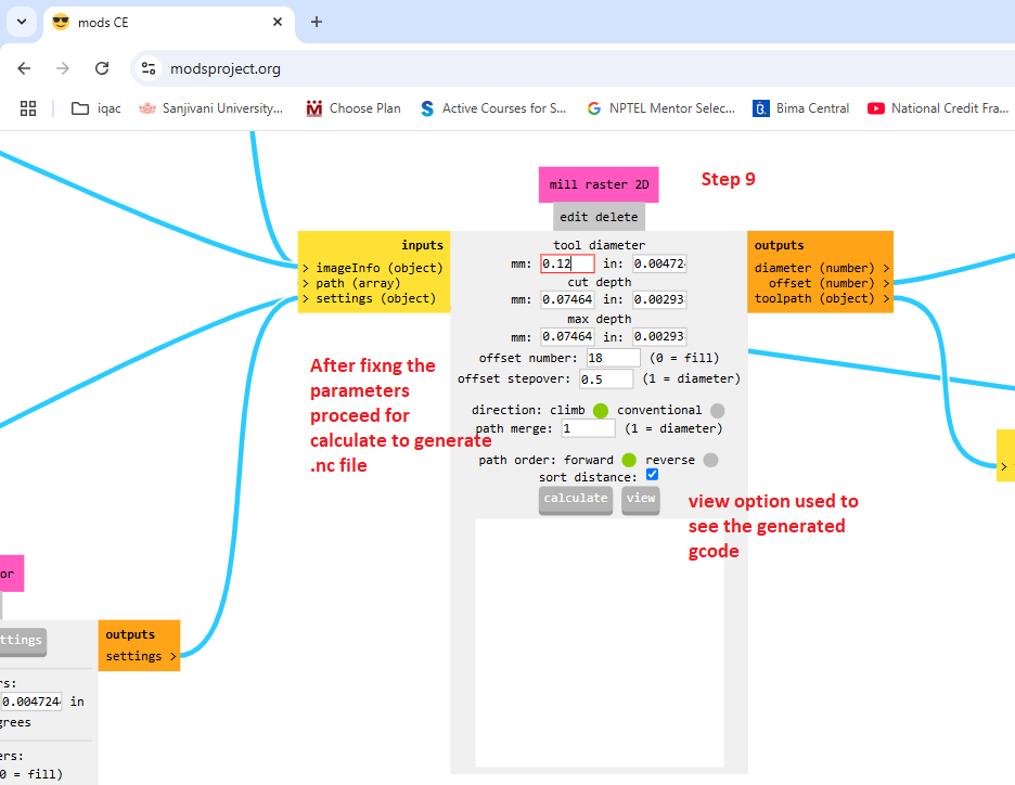
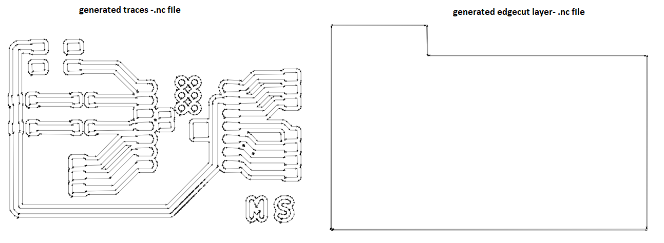
Calculated the .nc file view in Mill raster 2D option for FCu traces and Edge cut layers
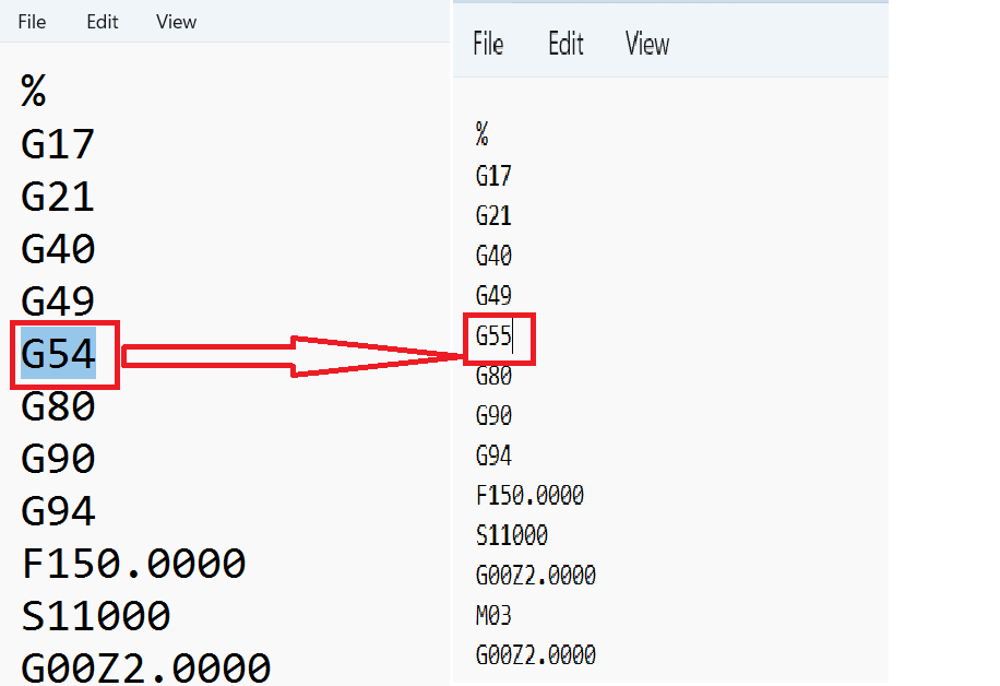
After downloading of .nc file modified the file name extension from .nc to .gcd format and opened the file changes G54 to G55 in the generated file as per machine requirements
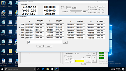
Set the origin of the machine after placing the pcb board
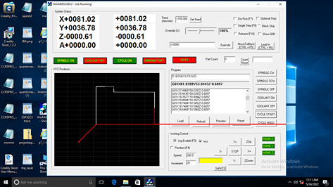
Upload the file to software, able to see in progress window and PCB milling video shown below
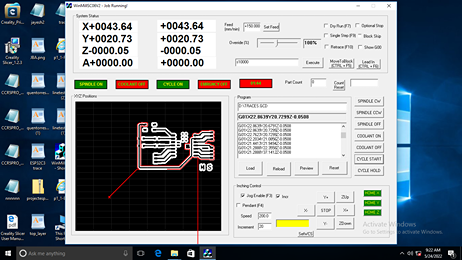
After loading Edge cut file
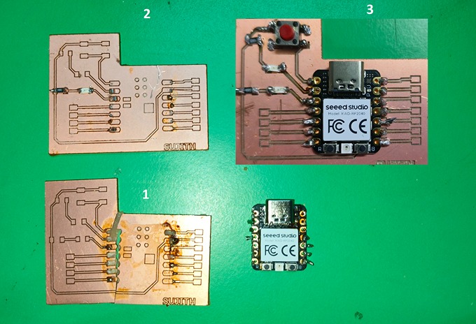
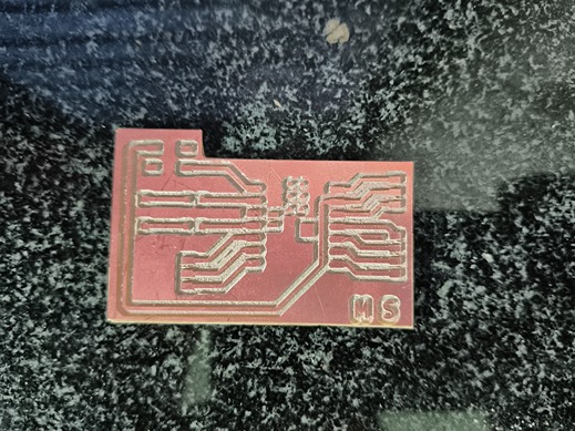
Final PCB engraved board
After Soldering of components pushbutton, led and resistor 50 ohm and header port for laying connections
Heroshots of my board
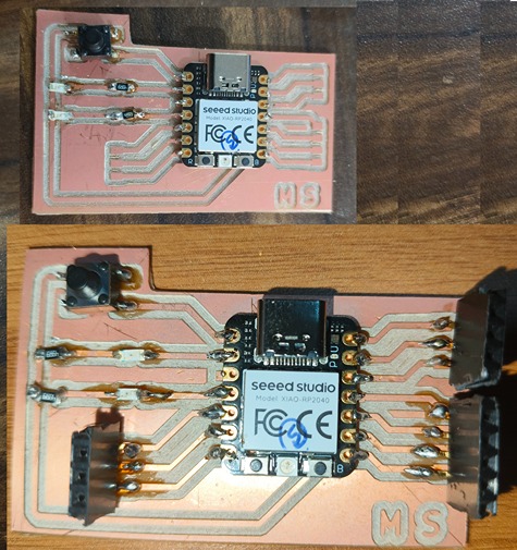
After completion of soldering i checked the XIAO RP 2040 by uploading the LED blinking code on port D1
Below program is uploaded to check the pcb
const int ledPin =  D1;

void setup() {
    pinMode(ledPin, OUTPUT);  // Set D0 as an output
}

void loop() {
    digitalWrite(ledPin, HIGH);  // Turn LED ON
    delay(1000);                  // Wait 1 second
    digitalWrite(ledPin, LOW);   // Turn LED OFF
    delay(1000);                  // Wait 1 second
}
Uploading the LED blinking code on Selecting D3, it works perfectly
Below program is uploaded to check the pcb
const int ledPin =  D3;

void setup() {
    pinMode(ledPin, OUTPUT);  // Set D0 as an output
}

void loop() {
    digitalWrite(ledPin, HIGH);  // Turn LED ON
    delay(1000);                  // Wait 1 second
    digitalWrite(ledPin, LOW);   // Turn LED OFF
    delay(1000);                  // Wait 1 second
}
Finally uploaded the pushbutton program, but it worked perfectly, there is mistake in the soldering, i used the multimeter to check the connectiivty and resoldered again
Below program is uploaded to check the pcb
#define LED_PIN D1 // LED connected to GPIO 13 (onboard LED)
#define BUTTON_PIN D0  // Push button connected to GPIO 2

bool ledState = false;

void setup() {
    pinMode(LED_PIN, OUTPUT);
    pinMode(BUTTON_PIN, INPUT_PULLUP); // Use internal pull-up resistor
}

void loop() {
    if (digitalRead(BUTTON_PIN) == LOW) {  // Button pressed (LOW due to pull-up)
        delay(200);  // Debounce delay
        ledState = !ledState;  // Toggle LED state
        digitalWrite(LED_PIN, ledState);
        while (digitalRead(BUTTON_PIN) == LOW); // Wait until button is released
    }
}