Week 8: Electronics Production
We have used the lab's test equipment to observe the operation of a microcontroller circuit board, demonstrating the use of a multimeter and oscilloscope. The work has been documented on the group work page, with individual reflections recorded on our personal pages.
Visit our Group Assignment Page to explore our findings and methodologies.
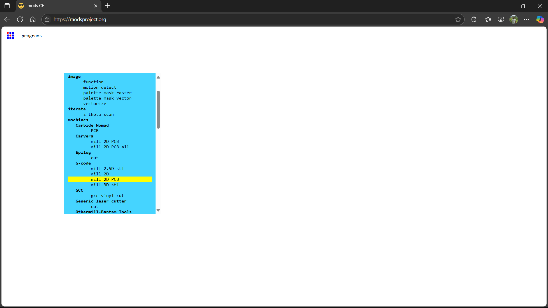
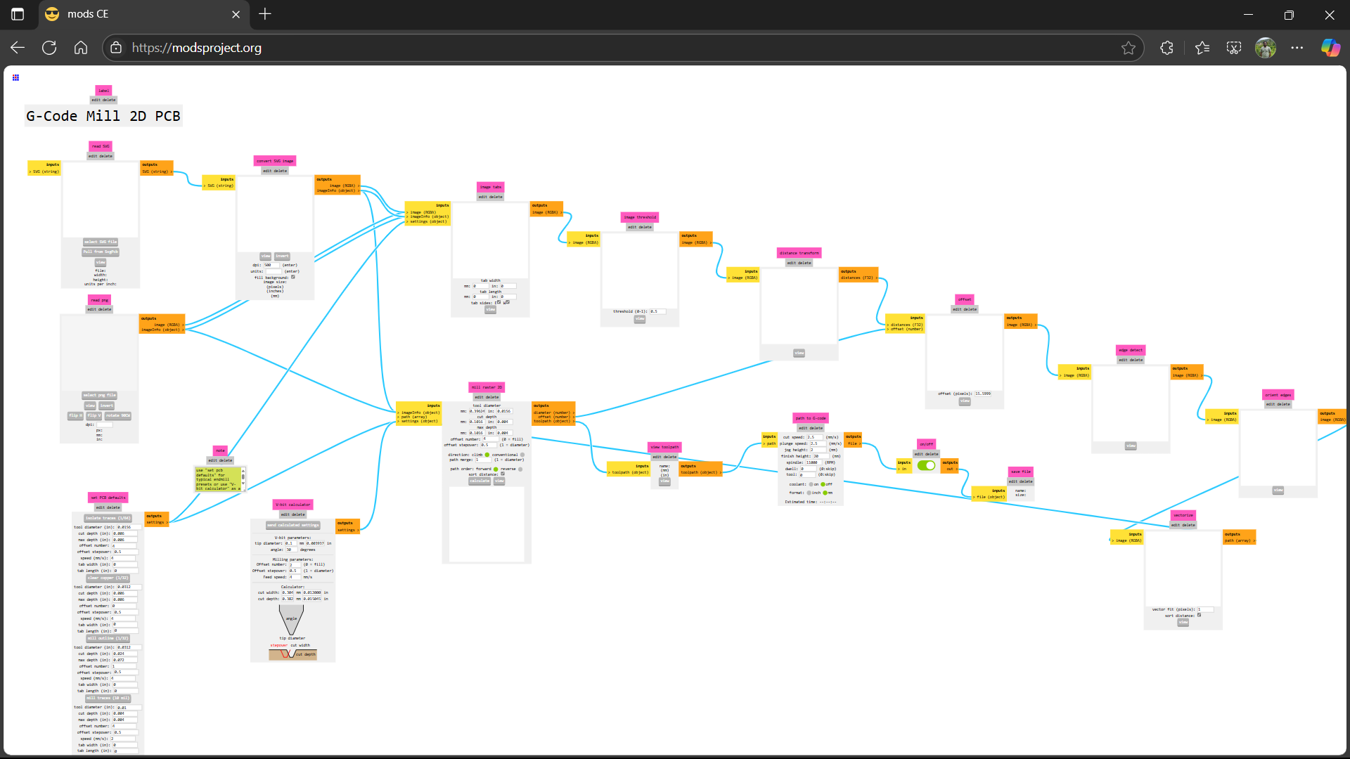
1. Toolpath Generation
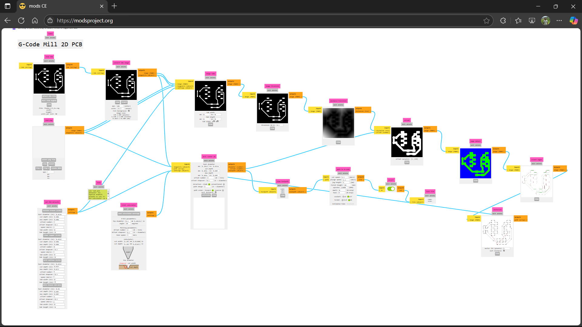
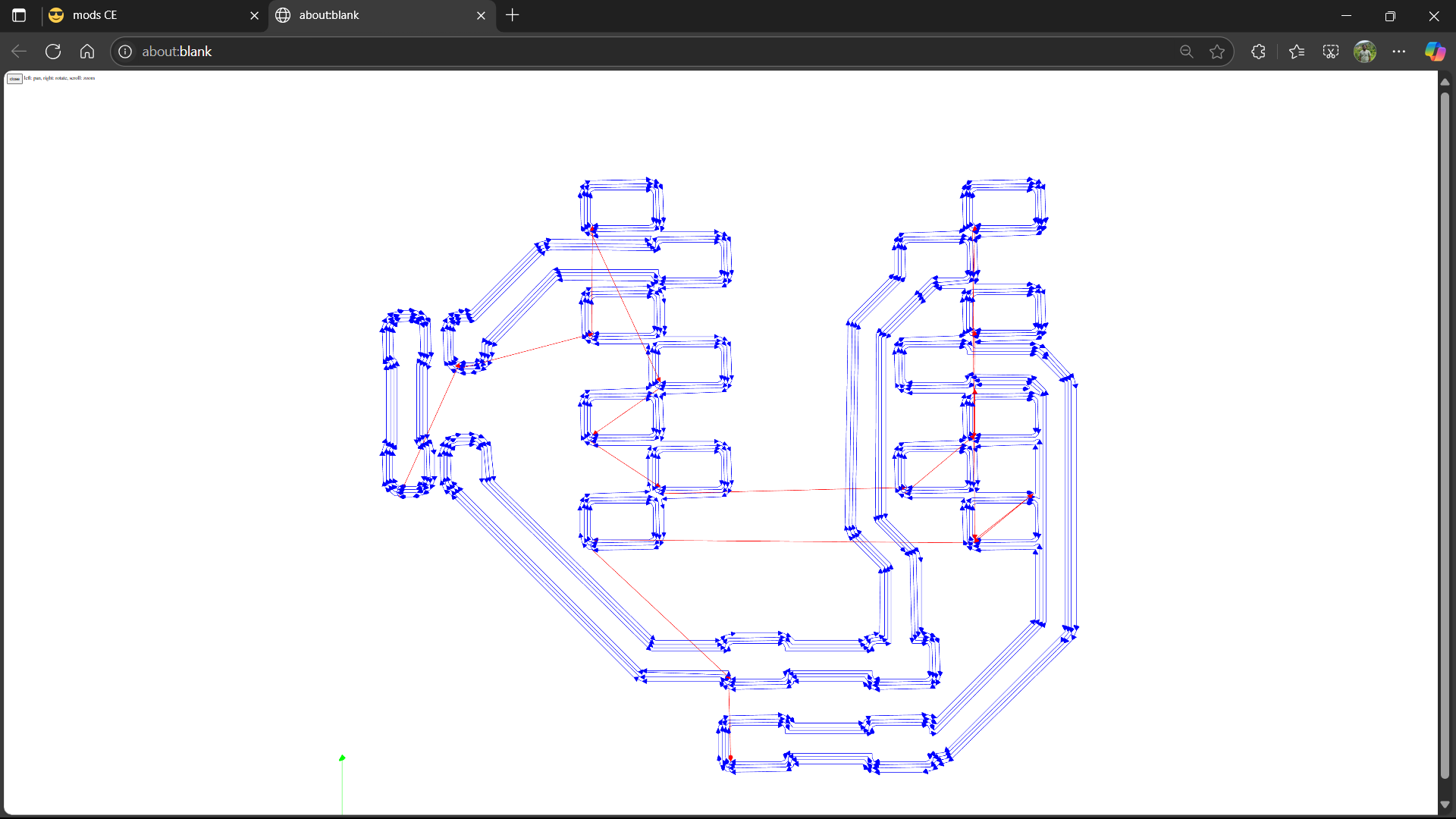
Generating an accurate and efficient toolpath is a critical step in PCB fabrication, ensuring precise milling and a functional end product. Using Mods, an open-source and modular software platform, we carried out the process systematically to achieve the desired results. Here is a detailed breakdown of how the toolpath generation was executed:
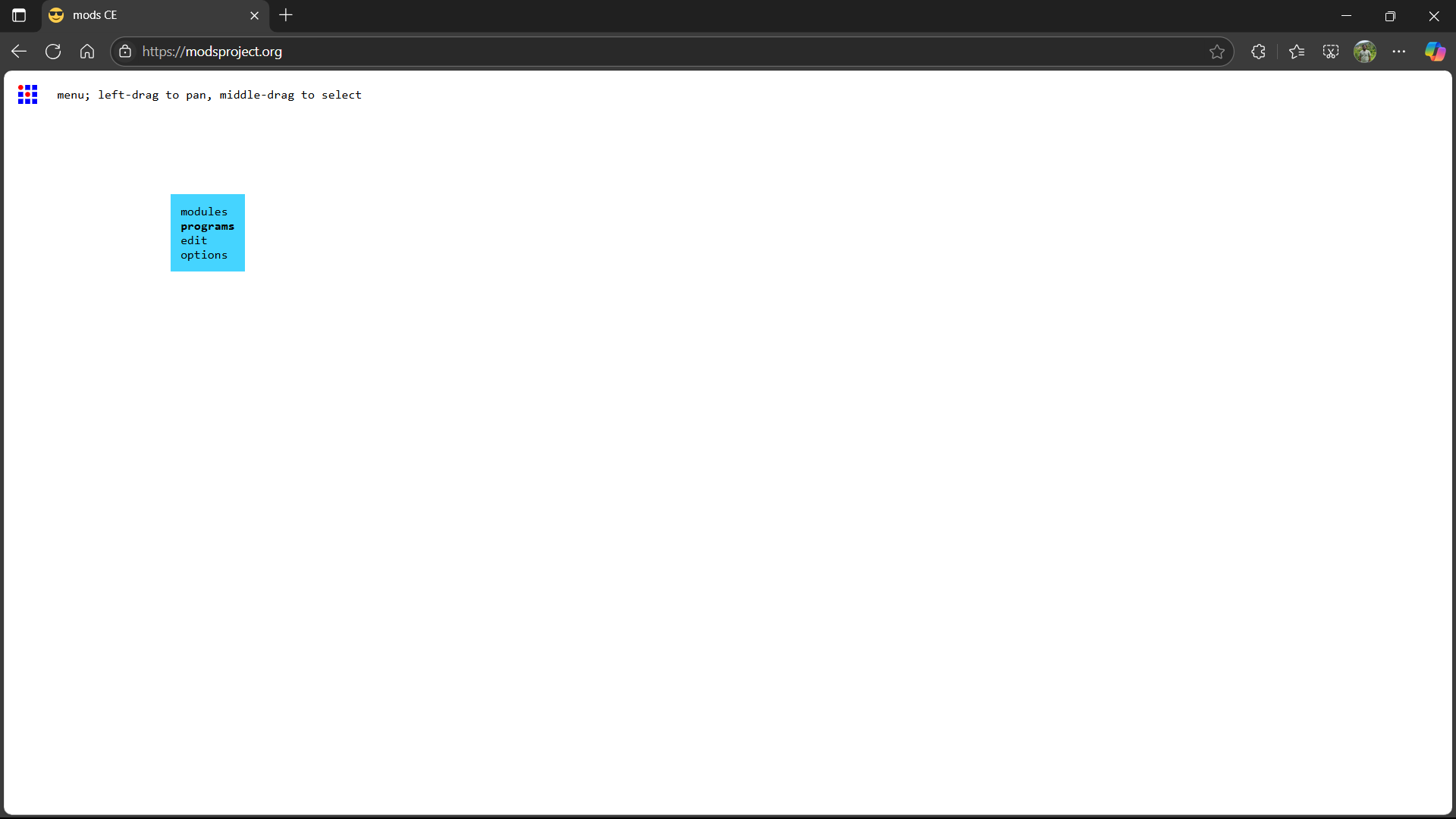
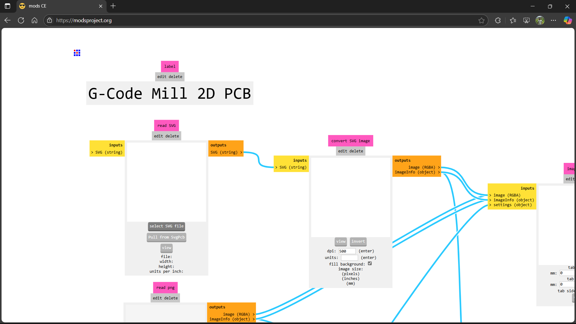
- Software Used: Mods was chosen for its versatility and suitability for PCB milling. Unlike conventional CAM software, Mods allows for modular configurations, enabling users to create a customized workflow tailored to their specific requirements. Its open-source nature also makes it highly adaptable, with features that cater to both simple and complex designs. The software was accessed via a web browser, and its intuitive interface made it easy to upload the design files and begin the toolpath generation process.
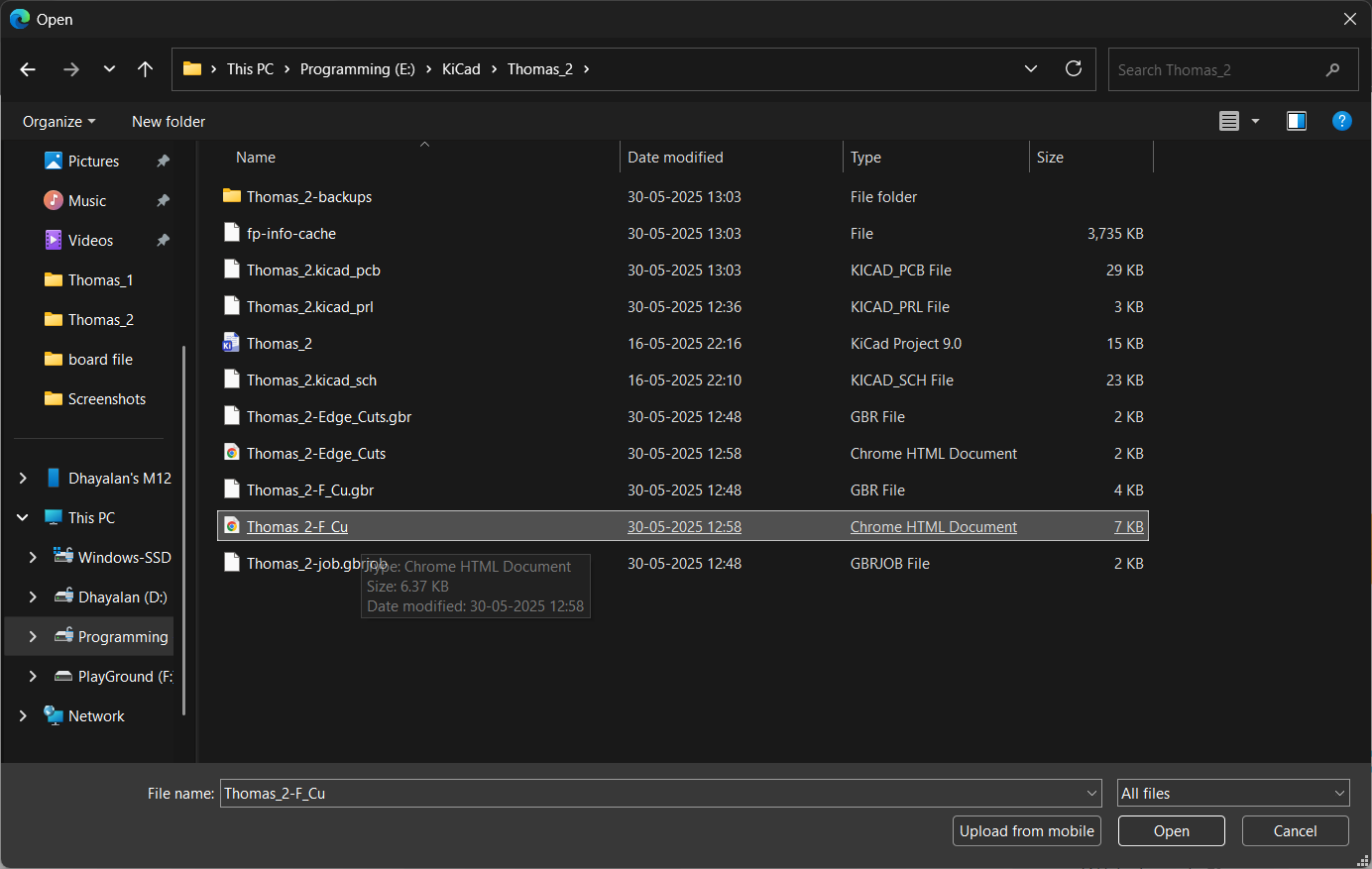
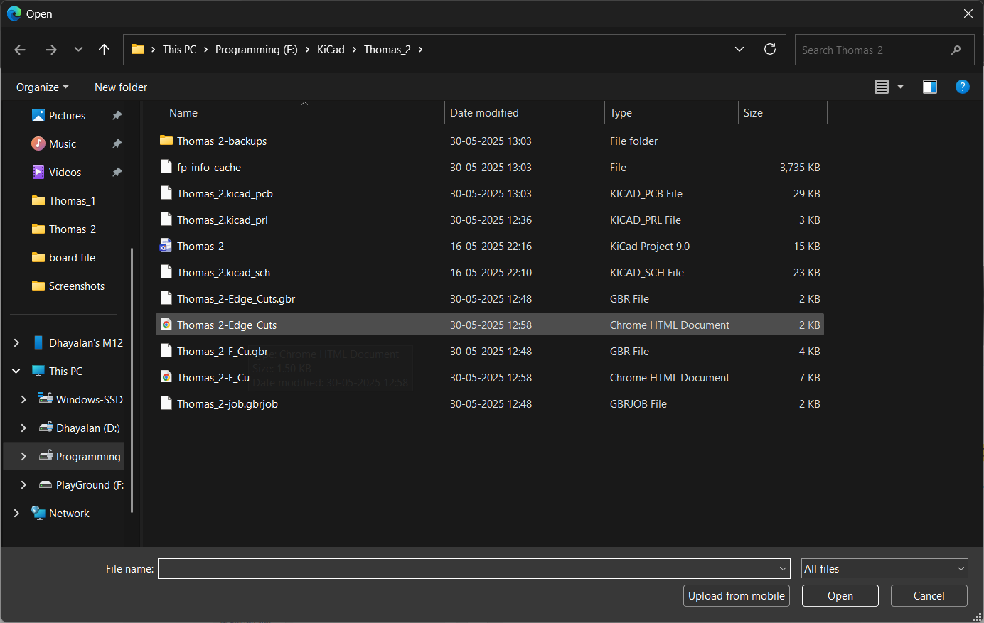
- File Preparation: Before starting with Mods, the PCB design was finalized using KiCad. The Gerber files generated from KiCad, which include copper layers, solder masks, and drill files, were imported into Mods. These files form the foundation for the toolpath generation. The design was checked thoroughly for errors or inconsistencies before proceeding to avoid any complications during milling.
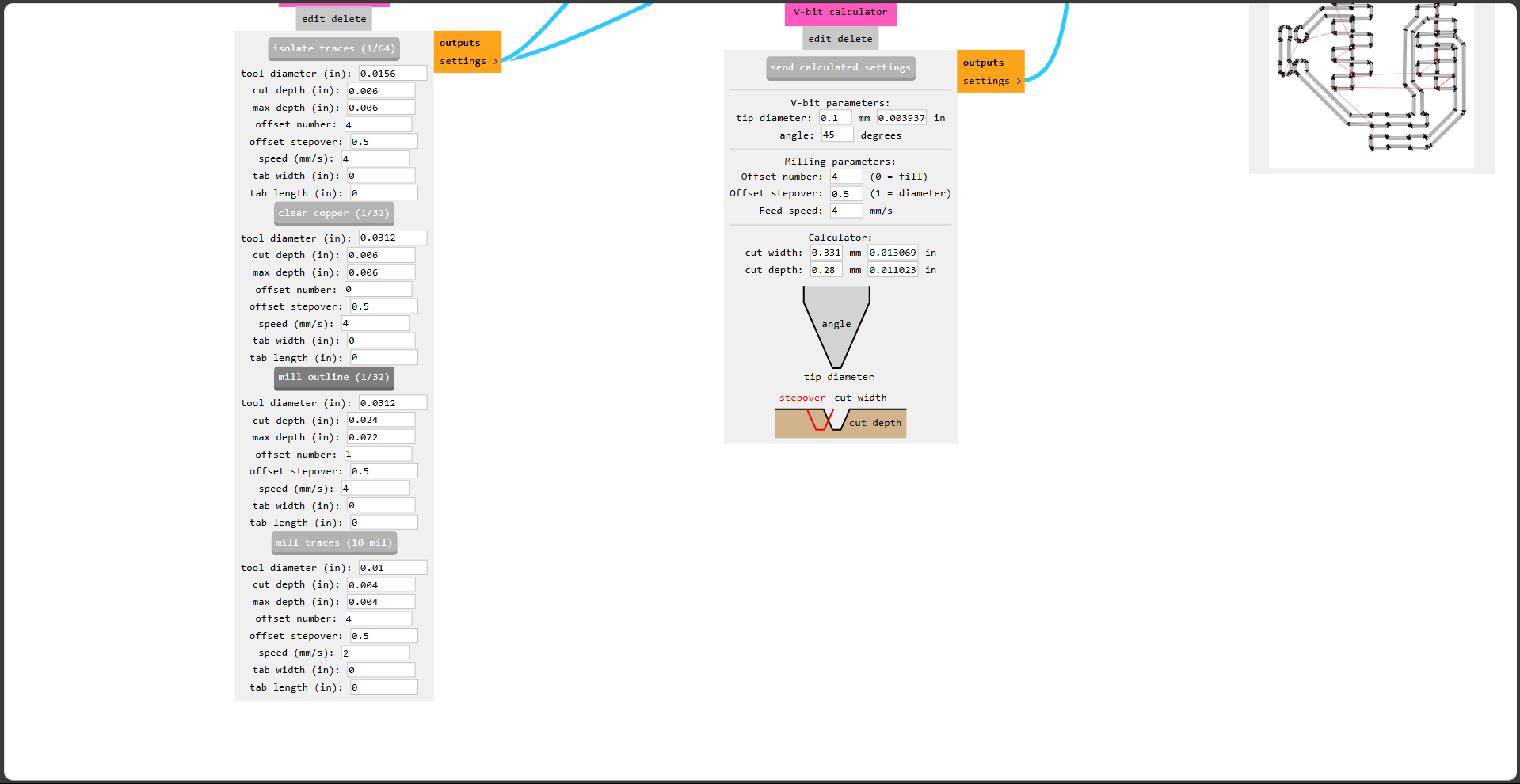
- Trace Width Definition: One of the critical steps in toolpath generation is defining the trace widths. In Mods, this was done by specifying the desired line thickness that corresponds to the design. Proper trace width ensures that the electrical paths on the PCB are neither too thin, which could lead to breaks, nor too thick, which could result in shorts or unnecessary material removal. This step was particularly important for maintaining the electrical integrity of the circuit.
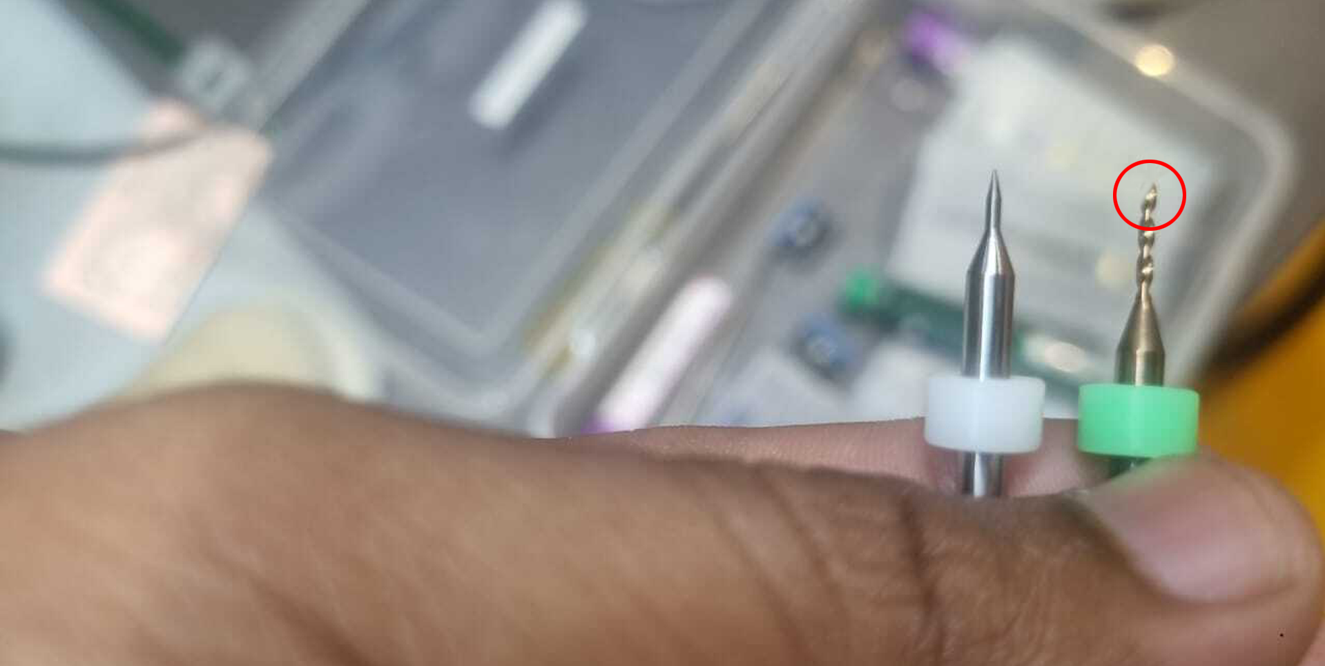
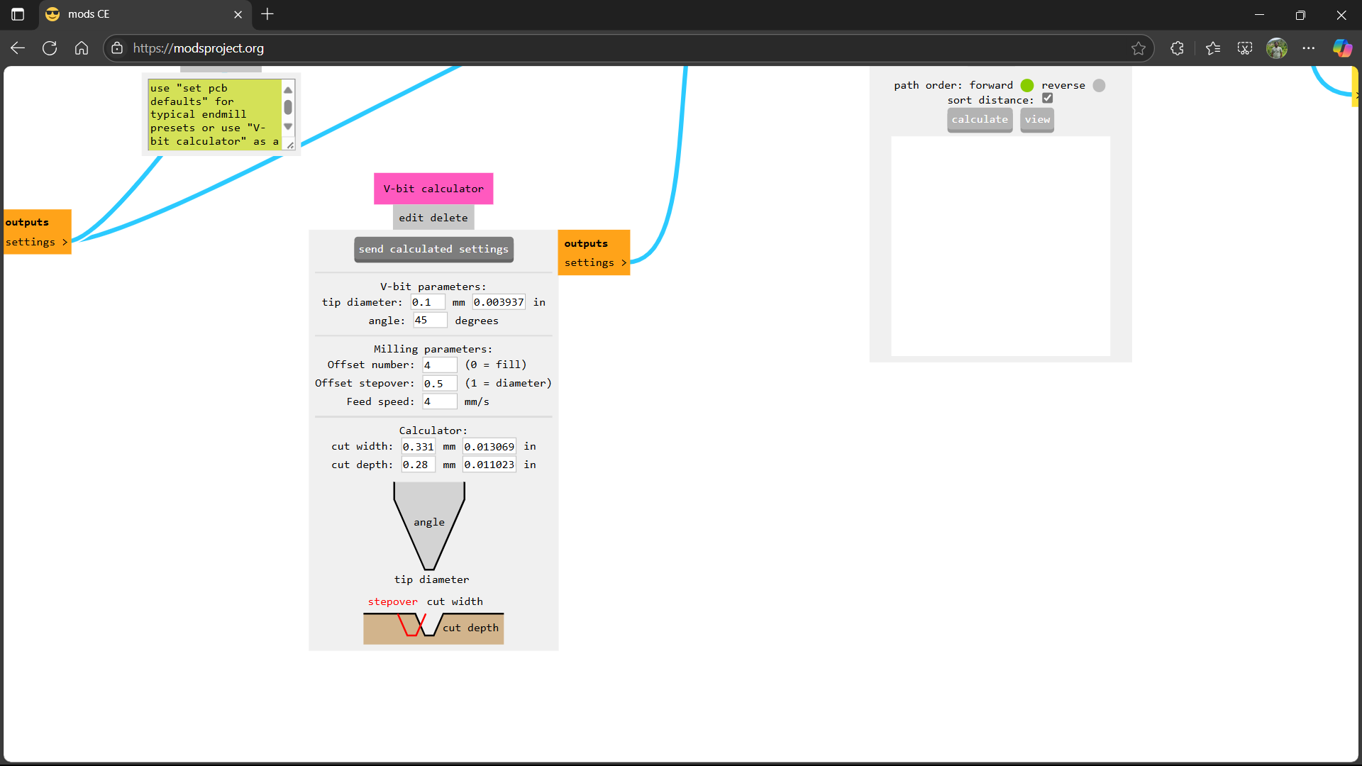
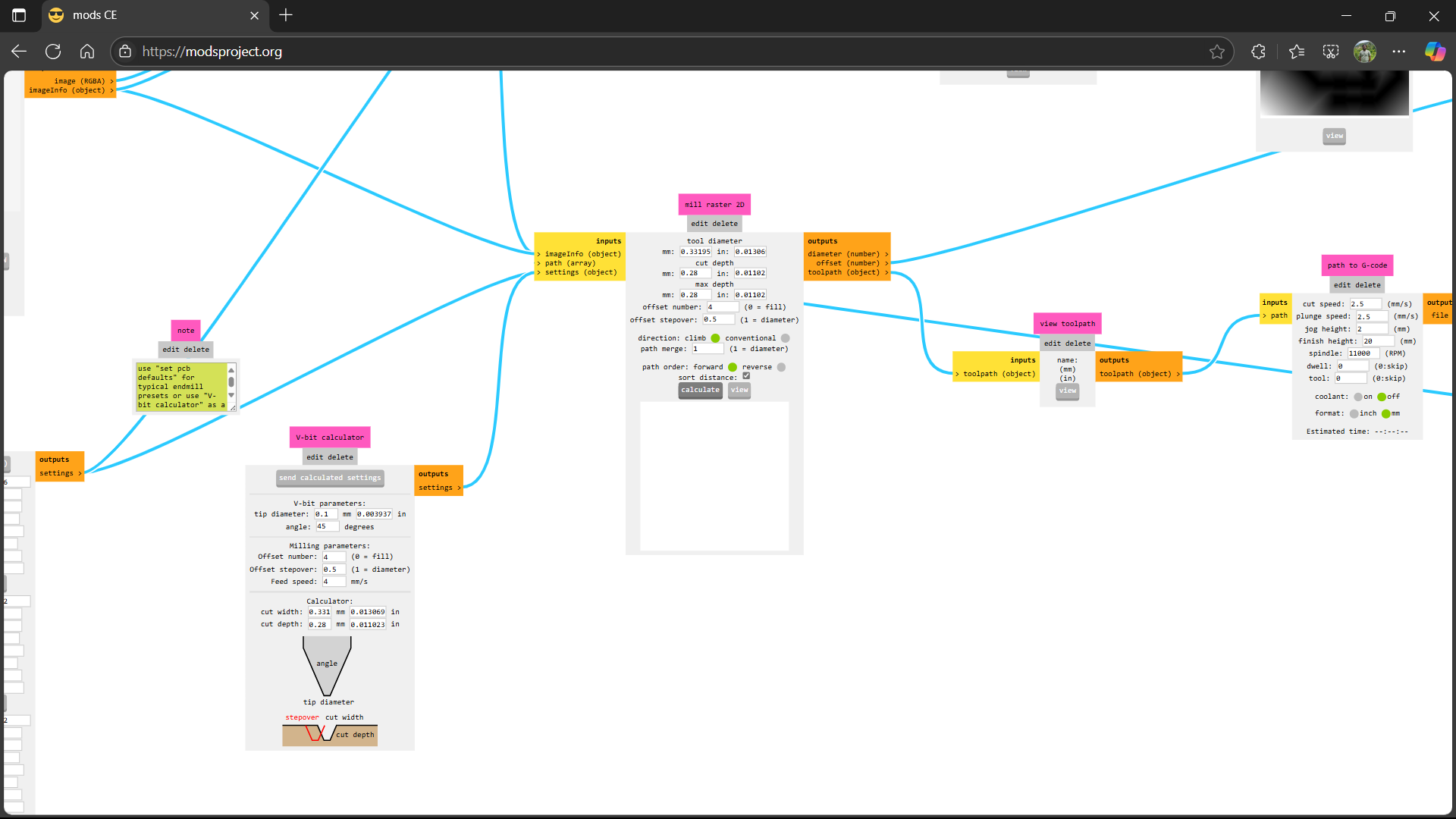
- Tool Selection: The choice of tools for milling was based on the design requirements and material properties. A fine-tipped end mill was selected for detailed work, such as cutting traces and vias. Mods provided the flexibility to input tool parameters such as diameter, cutting speed, and feed rate, which were adjusted to match the PCB material and ensure precise cuts without damaging the tools.
- Setting Milling Depth: Accurate milling depth is essential to ensure that the tool cuts through the copper layer without penetrating too deeply into the substrate. Mods allowed for precise control over the cutting depth, with parameters set based on the thickness of the PCB material. Multiple passes were programmed for deeper cuts to avoid tool stress and maintain precision.
- Toolpath Strategy: Mods supports various toolpath strategies, including isolation milling, pocketing, and drilling. For this project, isolation milling was used to separate the traces from the surrounding copper, while pocketing was applied for larger areas that needed to be cleared. Drill toolpaths were generated for vias and through-holes. The strategies were configured to optimize material removal while minimizing machining time.
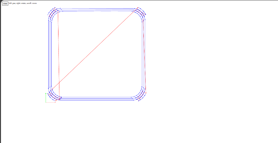
- Simulation: Before actual milling, the generated toolpath was simulated within Mods. The simulation feature provided a visual representation of how the milling would progress, highlighting any potential issues such as uncut areas, tool collisions, or excessive material removal. Adjustments were made based on the simulation results to refine the toolpath and ensure accuracy.
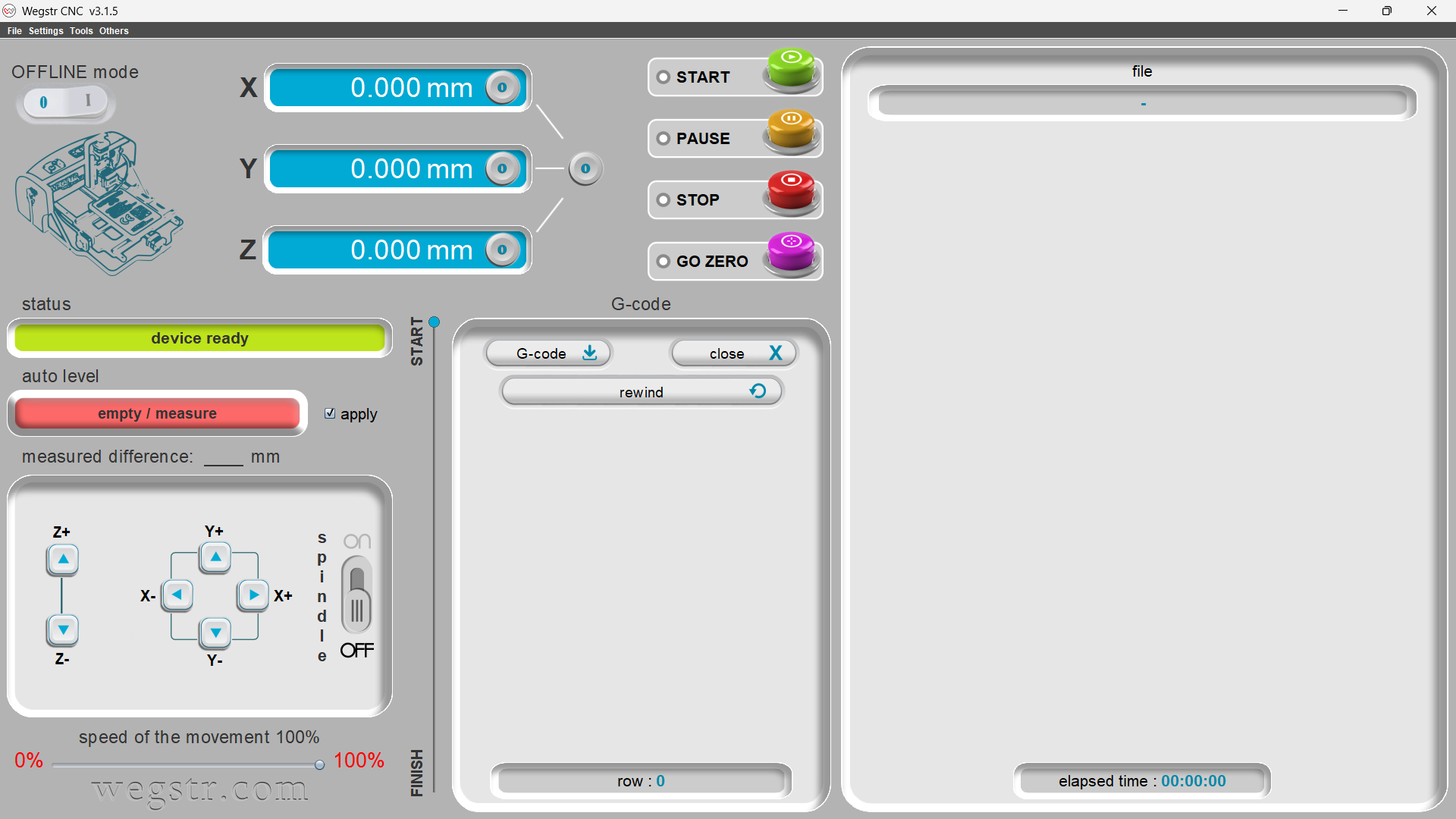
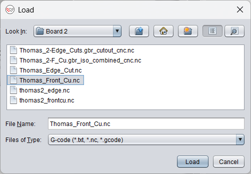
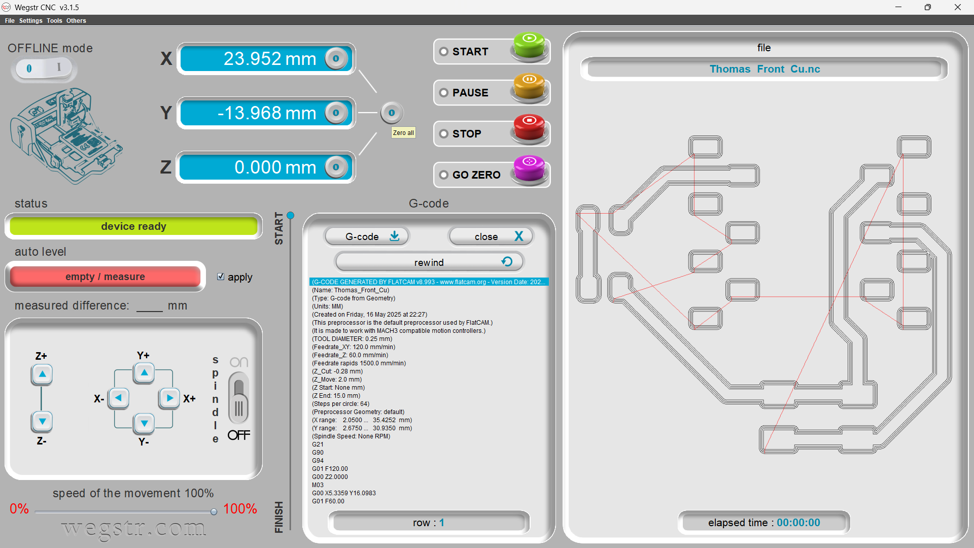
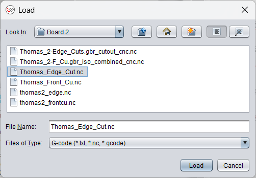
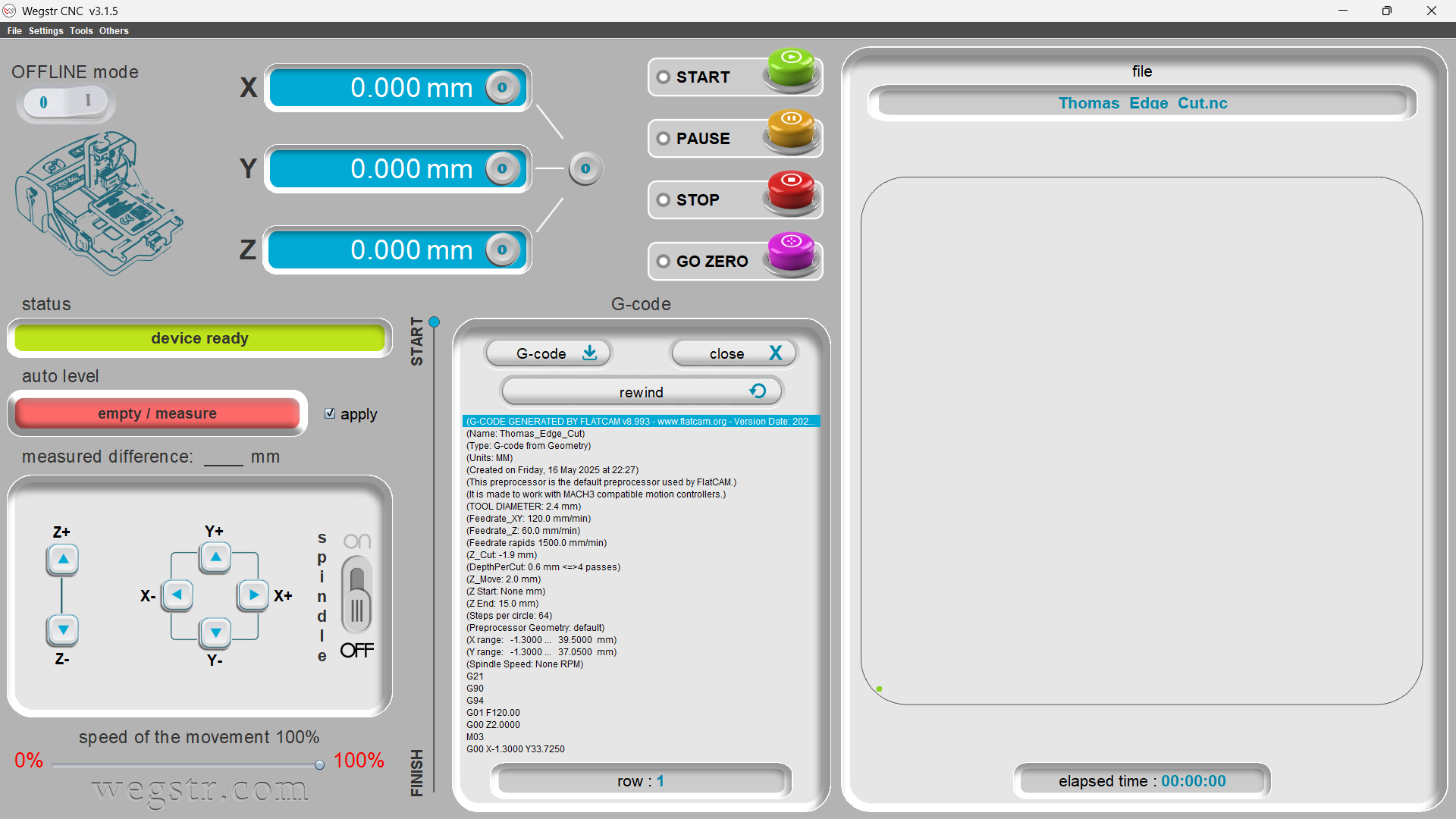
- Exporting the Toolpath: Once the toolpath was finalized, it was exported in a format compatible with the CNC milling machine. Mods supports various file formats, making it easy to integrate with different types of machines. The toolpath file was saved and transferred to the milling machine for execution.
- Error Handling: During the process, some minor errors were encountered, such as incomplete traces or overlapping toolpaths. These issues were resolved by revisiting the design in KiCad and re-importing the corrected files into Mods. This iterative approach ensured that the final toolpath met all design specifications.
- Testing and Verification: After generating the toolpath, test runs were performed on scrap material to verify the accuracy of the cuts. This step helped confirm that the settings in Mods were correct and that the toolpath would produce the desired results. Any necessary adjustments were made before proceeding with the actual PCB material.
Using Mods for toolpath generation proved to be a robust and effective approach for this project. Its modular design allowed for complete customization of the workflow, while its powerful simulation and error-handling features ensured a smooth and accurate milling process. By carefully following each step and addressing any issues promptly, we were able to create a precise toolpath that met the requirements of our PCB design.
2. Making the Board
The process of creating a printed circuit board (PCB) involves three main stages: milling the board to define its structure, placing components (stuffing), and soldering the components to create a functional electronic assembly. Each stage requires precision, attention to detail, and the right tools to achieve a high-quality result. Below is a detailed walkthrough of how the board was made.
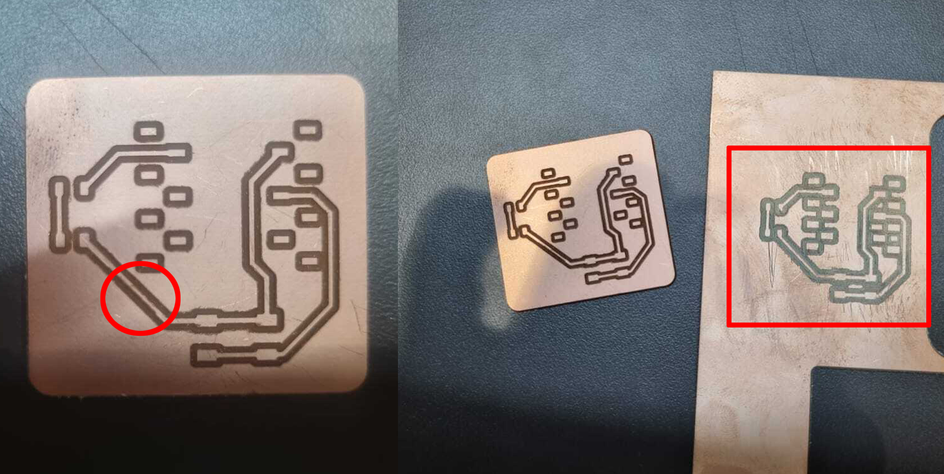
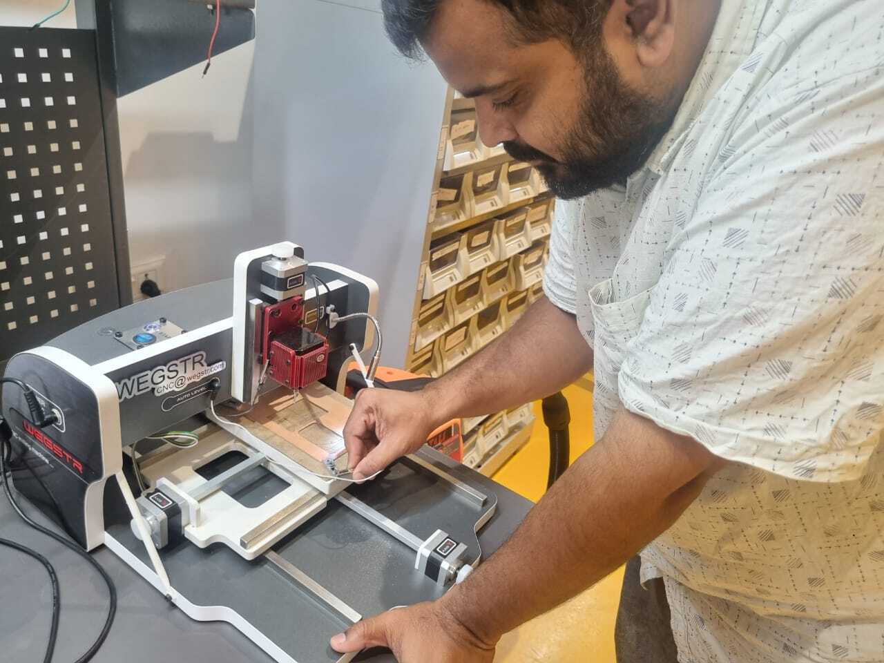
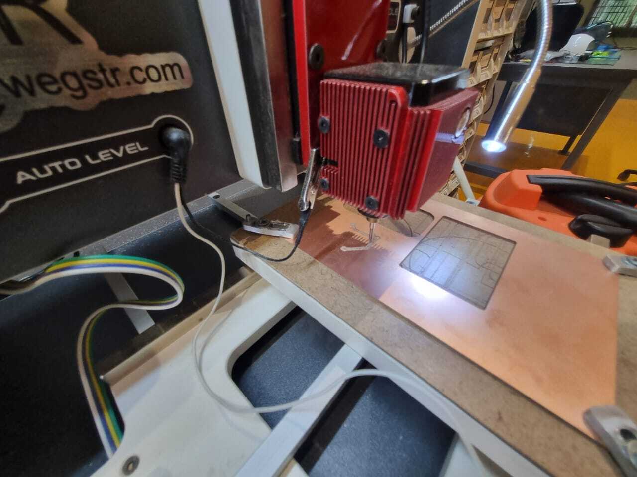
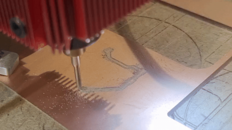
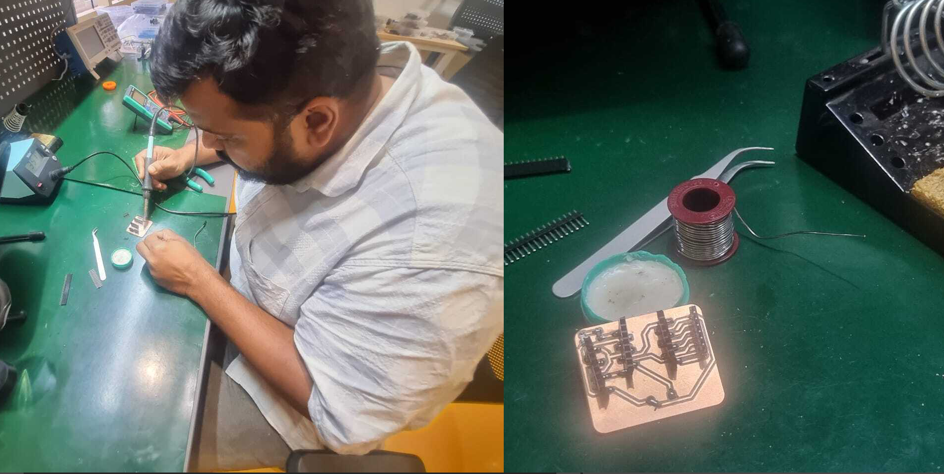
- Milling: Milling is the first step in fabricating a PCB, and it involves using a CNC milling machine to cut the copper traces and shape the board. The process begins by mounting a blank PCB onto the machine bed, ensuring it is flat and secure. The toolpath generated in the previous step was uploaded to the CNC machine. The machine was calibrated by zeroing the Z-axis to ensure the cutting tool would accurately penetrate the copper layer without damaging the substrate beneath. Multiple passes were made, starting with a shallow depth to outline the traces and drilling holes for through-hole components. Once the traces were complete, a separate toolpath was used to cut out the board's perimeter. Milling required constant monitoring to ensure the cutting tool did not wear out or misalign during the process. After the milling was complete, the board was inspected to confirm the traces were cleanly cut and aligned with the design. Any residual burrs were carefully sanded away to ensure smooth edges.
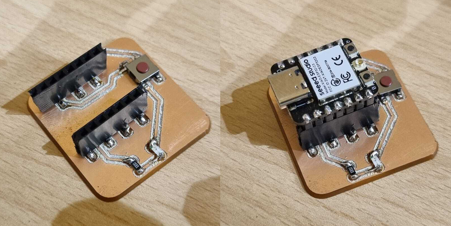
- Stuffing: After milling, the next step was placing components onto the board, a process known as stuffing. Each component, such as resistors, capacitors, LEDs, and ICs, was identified and matched to its designated position on the PCB based on the schematic. Components were arranged in an orderly manner to avoid confusion during soldering. To ensure accuracy, small tweezers were used to handle the delicate components, especially the smaller ones like surface-mount devices (SMDs). Polarized components, such as diodes and electrolytic capacitors, were double-checked to ensure they were oriented correctly according to their polarity markings on the board. Stuffing also involved verifying the alignment of ICs with their notches or dot indicators to match the corresponding silkscreen on the PCB. Care was taken to insert pins into the correct vias to prevent functionality issues.
- Soldering: Soldering is the final stage of making the board, where the components are securely attached to the PCB. A soldering iron with a fine tip was used for precision, and lead-free solder was chosen to meet environmental standards. The process began by heating each component lead and its associated pad on the PCB. A small amount of solder was applied, forming a strong, shiny joint that ensured electrical conductivity. Care was taken to avoid overheating the components, which could damage them or cause the solder to flow unevenly. Common soldering issues, such as cold solder joints (caused by insufficient heat) or solder bridges (unintended connections between adjacent pads), were meticulously avoided. In areas where solder bridges were detected, a solder wick or desoldering pump was used to remove excess solder and clean up the joints. For through-hole components, solder was applied to the underside of the board, ensuring that it fully covered the pads while remaining smooth and uniform. Surface-mount components required a slightly different technique, often using a reflow process or solder paste to achieve a clean finish. After soldering, the board was visually inspected under a magnifying glass to ensure all joints were intact and free from defects. A multimeter was also used to check for continuity, confirming that all connections were properly established.
The entire process of making the board was carefully documented to ensure reproducibility and to identify potential areas for improvement in future projects. From milling the traces to soldering the components, every step required careful planning and execution to create a fully functional PCB. The resulting board was tested for functionality, and any errors encountered during testing were promptly addressed.
3. Functional Testing
Functional testing is a critical phase in the PCB development process, ensuring the board operates as designed. This stage involves verifying power supply functionality, testing the input/output components, and uploading test programs to confirm that all elements of the board work seamlessly. Below is an in-depth account of how the board was tested.
- Power-On Test: The first step in functional testing was the power-on test, aimed at verifying that the board powers on correctly without any short circuits or unexpected behavior. A regulated power supply was connected to the board, and the current draw was monitored using a multimeter. If the board exhibited any signs of excessive current draw, indicating a possible short circuit, it was immediately powered off to avoid damage. The problem area was then identified and rectified. Once the board passed the power-on test, the voltage at various test points was measured to confirm that all components were receiving the correct supply voltage. LEDs connected to power rails served as visual indicators, lighting up to confirm proper voltage levels.
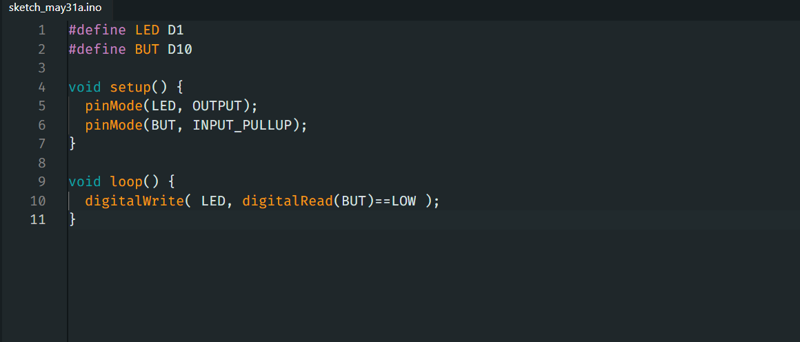
- Input/Output Test: Next, the board's input/output (I/O) functionality was tested. Each general-purpose input/output (GPIO) pin was probed using a logic analyzer to confirm that the signals were consistent with the design specifications. For digital I/O pins, test signals were sent to the board, and the output was monitored to ensure accurate response. Pull-up and pull-down resistors were checked to confirm proper logic levels. For analog inputs, varying voltage signals were applied to verify the microcontroller’s ADC (Analog-to-Digital Converter) functionality. Serial communication ports such as UART, I2C, or SPI were tested using appropriate devices to establish communication with external peripherals. For example, an I2C sensor was connected, and its data output was read to confirm successful communication. Similarly, the SPI interface was tested by connecting an external EEPROM and verifying data transfers. Any discrepancies in the output signals were resolved by rechecking connections and firmware configurations.
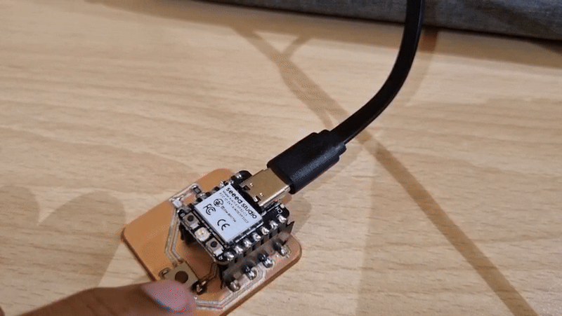
- Programming Test: The final phase of functional testing involved uploading a test program to confirm the microcontroller's operation. The microcontroller's programming port was connected to a computer via an appropriate interface, such as a USB-to-UART converter or an in-circuit programmer. A simple test program, such as one that blinked an LED or read a button press, was written and uploaded to the board. This test ensured that the microcontroller could successfully execute instructions and interact with the connected peripherals. Debugging tools, such as a JTAG debugger or a serial monitor, were used to monitor real-time data and outputs. If the microcontroller failed to respond, the issue was diagnosed by checking the firmware, connections, and configuration settings. In cases where the microcontroller required a bootloader, it was first installed to facilitate easy programming.
Throughout the testing process, careful documentation was maintained to record test conditions, expected outcomes, and observed results. This documentation served as a reference for troubleshooting and improving future iterations of the board.
After passing all functional tests, the board was deemed ready for deployment in its intended application. Testing not only validated the design but also provided valuable insights into optimizing the manufacturing process and ensuring reliability in real-world use cases.
4. Problems and Fixes
Throughout the project, several challenges arose, each providing valuable learning opportunities. Below is a comprehensive account of the problems encountered and the strategies employed to resolve them.
- Problem: Misaligned traces during milling.
Details: One of the primary issues faced during the milling process was the misalignment of traces on the PCB. This occurred because the material was not secured properly, causing slight shifts during the machining process. Misaligned traces can lead to broken connections, rendering the board unusable.
Solution: The problem was addressed by ensuring that the material was firmly clamped to the CNC milling machine’s bed. Double-sided tape was also used as an additional securing mechanism to prevent any movement. The toolpath was recalculated and realigned using precision alignment features in the CAM software. Finally, test runs were conducted on a scrap piece of material to confirm proper alignment before proceeding with the actual board. - Problem: Solder bridges on fine-pitch ICs.
Details: While soldering fine-pitch ICs, solder bridges formed between adjacent pins, causing unintended electrical connections. This issue is common when working with small components and can result in short circuits.
Solution: Solder bridges were resolved using a solder wick to absorb excess solder. A magnifying lamp was used to carefully inspect each pin, ensuring that all connections were clean and free of bridging. Additionally, the soldering iron’s tip was cleaned and tinned to enhance precision. Flux was applied to improve solder flow, and a finer soldering tip was used for better control. For subsequent attempts, a stencil and reflow soldering process were employed to achieve consistent results. - Problem: Microcontroller not responding.
Details: After completing the assembly, the microcontroller failed to respond during the initial programming test. This issue was traced to an unstable power supply circuit and a missing bootloader.
Solution: The power supply circuit was debugged by measuring voltage levels at different points on the board. A faulty voltage regulator was identified and replaced, stabilizing the supply. The bootloader was then reprogrammed using an in-circuit programmer. Additionally, all connections were rechecked to ensure continuity. To avoid similar issues in the future, extra care was taken to validate the power circuit during schematic design and layout stages. - Problem: Incorrect component placement.
Details: During assembly, some components were placed in the wrong orientation, particularly polarized components like diodes and capacitors. This mistake led to circuit malfunctions.
Solution: The incorrectly placed components were identified through careful inspection and testing. They were desoldered and replaced in the correct orientation. To minimize such errors, component placement was cross-referenced with the design files before soldering. Clear labeling on the PCB layout was also added to guide proper placement. - Problem: Noise in signal lines.
Details: During functional testing, high levels of noise were detected on some signal lines, affecting the performance of analog and communication circuits.
Solution: Decoupling capacitors were added close to the affected components to filter out noise. Signal traces were rerouted to minimize crosstalk and interference. Shielding techniques, such as using ground planes and avoiding long parallel traces, were implemented in the design. These changes significantly reduced the noise levels. - Problem: Components not fitting correctly.
Details: Some components did not fit properly into the PCB due to incorrect footprint dimensions in the design.
Solution: The footprints were re-verified against the component datasheets. Any mismatched components were desoldered, and the PCB was manually adjusted to accommodate them. The design files were updated to include accurate footprints for future iterations.
Each of these challenges underscored the importance of thorough planning and meticulous execution. By addressing these problems systematically, the project not only achieved its objectives but also provided a valuable hands-on experience in troubleshooting and problem-solving.
These experiences emphasize the iterative nature of PCB design and assembly, where each challenge brings insights that enhance future projects. With these lessons, subsequent designs will incorporate improved practices, ensuring higher quality and reliability.