Introduction To PCB Production
The electronics manufacturing process involves assembling electronic components and parts through electronic and mechanical assembly to create products that meet design requirements. Printed Circuit Boards (PCBs) are the backbone of most electronic devices, providing the necessary electrical connections between components
PCB Production Workflow
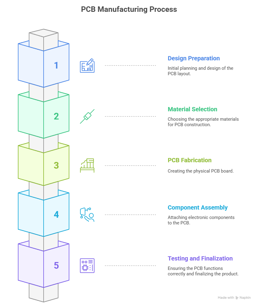
- Design Preparation
- Design Files: The process begins with design files, typically in formats such as SVG for front copper and edge cuts.
- File Conversion: The SVG file is converted into G-code using a tool like Mods CE (Community Edition), a web-based software for digital fabrication workflows. This conversion allows for precise control over tool paths, angles, and offsets required for PCB milling.
- Design Review: Key areas such as PCB pad design, trace width, and component locations are checked for defects. Additional considerations include thermal management, mechanical or dimensional constraints, and provisions for testing.
- Material Selection
- Types of PCBs: PCBs come in various forms, including single-sided, double-sided, multi-layer, and flexible boards.
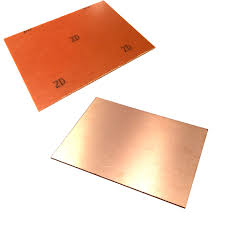
- Substrate Materials: The choice of substrate material is crucial. FR1 to FR4 are common materials, each with distinct properties.
- PCB Fabrication
- Milling: The G-code file is used to control a CNC milling machine. A copper-clad board (e.g., FR1) is securely fixed, and the machine engraves the circuit traces and cuts the board outline.
- Drilling: Holes for through-hole components are drilled as needed.
- Cleaning: After milling, the board is cleaned to remove dust and debris.
- Component Assembly
- Solder Paste Application: Solder paste is applied to the board using a stencil.
- Component Placement: Surface-mount components are placed using a pick-and-place machine.
- Reflow Soldering: The board passes through a reflow oven to melt the solder and secure components.
- Through-Hole Assembly: Through-hole components are inserted and soldered, either manually or using wave soldering.
- Inspection: The assembled board is inspected visually and using automated optical inspection (AOI) or X-ray for complex boards.
- Testing and Finalization
- Functional Testing: The board is powered and tested for correct operation.
- Documentation: A comprehensive Bill of Materials (BOM) and schematics are maintained for future reference and troubleshooting.
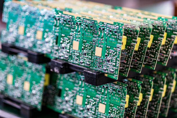
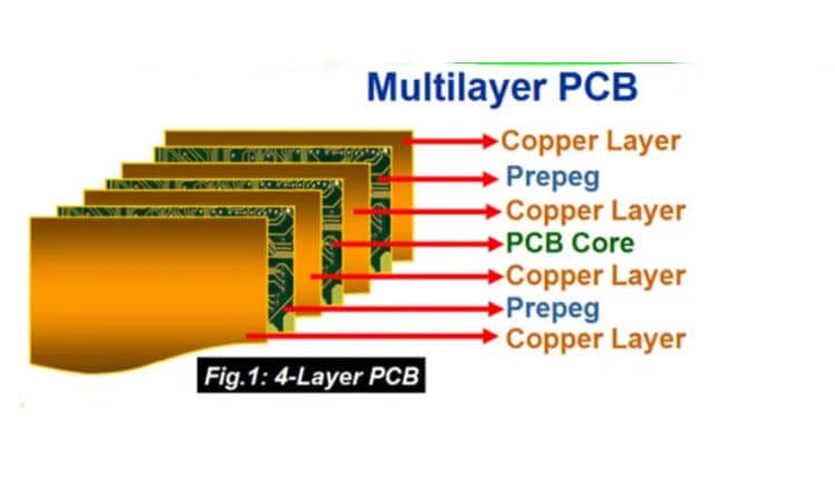
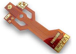
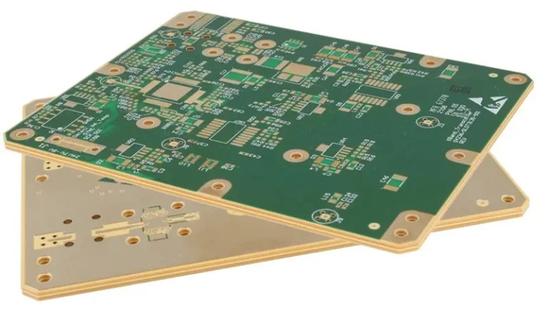
Types of PCBs
- Single-Sided PCBs: One layer of substrate with a conductive copper layer on one side. Components are mounted on one side, with traces on the opposite side.
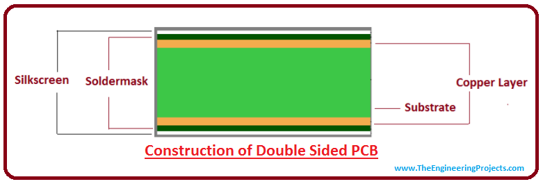
- Double-Sided PCBs: Copper layers on both sides of the substrate, allowing for more complex circuits.
- Multi-Layer PCBs: Multiple copper layers separated by insulating material, used for advanced electronics.
- Flexible PCBs: Made from flexible materials, used in applications where the board needs to bend.
PCB Substrate Materials: FR1 to FR4
FR1: Paper + Phenolic Resin
- Composition: Paper-based, coated with phenol-formaldehyde resin.
- Properties: Fire retardant, good mechanical strength, low cost, easy to handle.
- Applications: Single-layer PCBs, low-cost consumer electronics.
FR2: Cotton Paper + Phenolic Resin
- Composition: Cotton paper reinforced with phenolic resin.
- Properties: Enhanced over FR1, still low cost, suitable for less demanding applications.
FR3: Woven Fiberglass + Epoxy Resin
- Composition: Woven fiberglass mat embedded in epoxy resin.
- Properties: Improved electrical properties, higher temperature resistance (up to 170°C), lower loss tangent.
- Applications: Legacy industrial electronics, oscilloscopes, missile guidance systems.
FR4: Woven Fiberglass + Brominated Epoxy
- Composition: Woven fiberglass with brominated epoxy resin.
- Properties: Excellent electrical and mechanical properties, high temperature resistance (130–180°C), low loss tangent, self-extinguishing, high flexural strength.
- Applications: Industry standard for most modern electronics, including consumer, automotive, and aerospace products
PCB Production Process Flow
1. Circuit Transfer
The PCB manufacturing process begins by transferring the circuit layout onto the copper-clad substrate.
2. Solder Mask Application
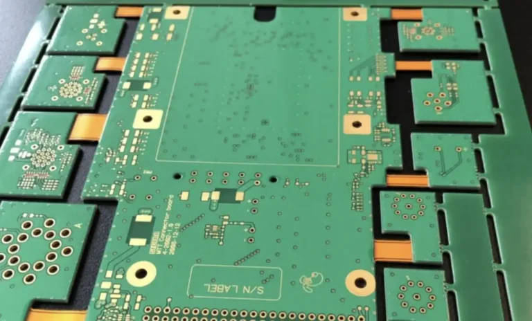
A solder mask is applied to the entire board surface, except for the areas where components will be soldered. This mask is typically green and provides insulation and protection against environmental factors.
3. Electrical Testing
For Electrical Testing of the milled PCB, a multimeter is used to check continuity between the tracks.This step ensures that there are no short circuits or unintended connections between traces.By performing this check before soldering components, potential damage to the components is prevented.This process helps maintain the reliability and safety of the final PCB assembly.
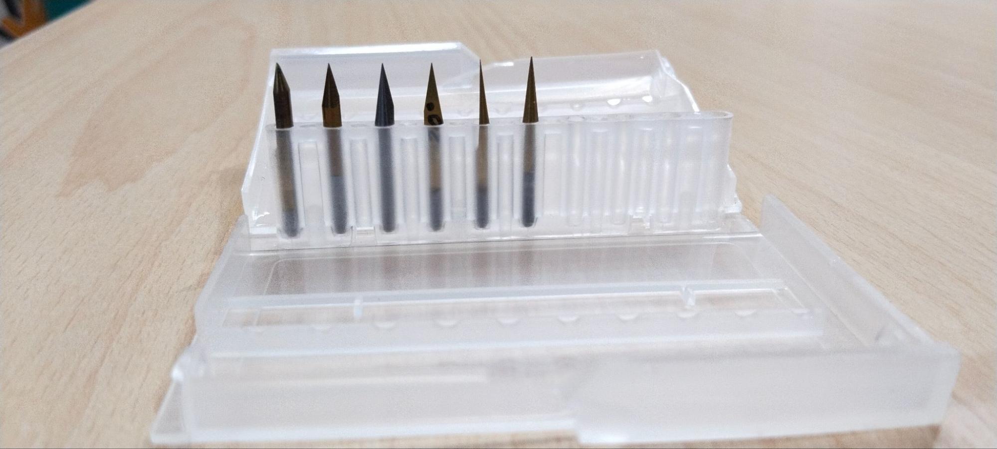
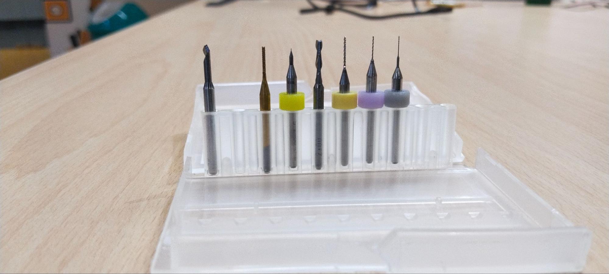
1. V-Shape Engraving/Isolation Bits (Common Angles: 10°, 20°, 30°, 45°, 60°)
- Main Feature: V-bit angle determines width and depth of cut—sharper angles (10°–20°) for fine detail.
- Application: Isolation routing to separate copper traces or engrave component outlines.
- Stage in Process: Used after drilling and before applying solder mask or components.
- Purpose: Avoids chemical etching by mechanically removing unwanted copper.
- Ideal Use: DIY PCB milling and prototyping with CNC machines.
2. Drill Bits (0.3 mm to 1.2 mm)
- Main Feature: Defined by diameter, not cutting angle.
- Application: Drilling via holes and component lead holes on the PCB.
- Size Selection: Based on the pin diameter of the components being mounted.
- Stage in Process: Used after copper layout design, before solder mask or component mounting.
- Purpose: Essential for creating electrical connections between top and bottom copper layers.
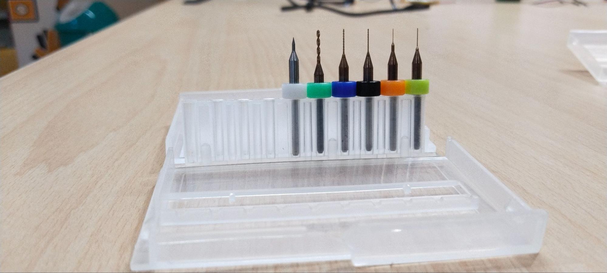
3. Spiral Drill Bits (1.05 mm to 1.3 mm)
- Main Feature: Similar to micro drill bits; no specific cutting angle emphasized.
- Application: Drilling larger holes for mounting screws or connector pins.
- Stage in Process: Used after micro holes, typically at the end of the drilling phase.
- Purpose: Supports mechanical assembly and interface connectors.
- Requirement: Used where strong, stable holes are needed on the PCB
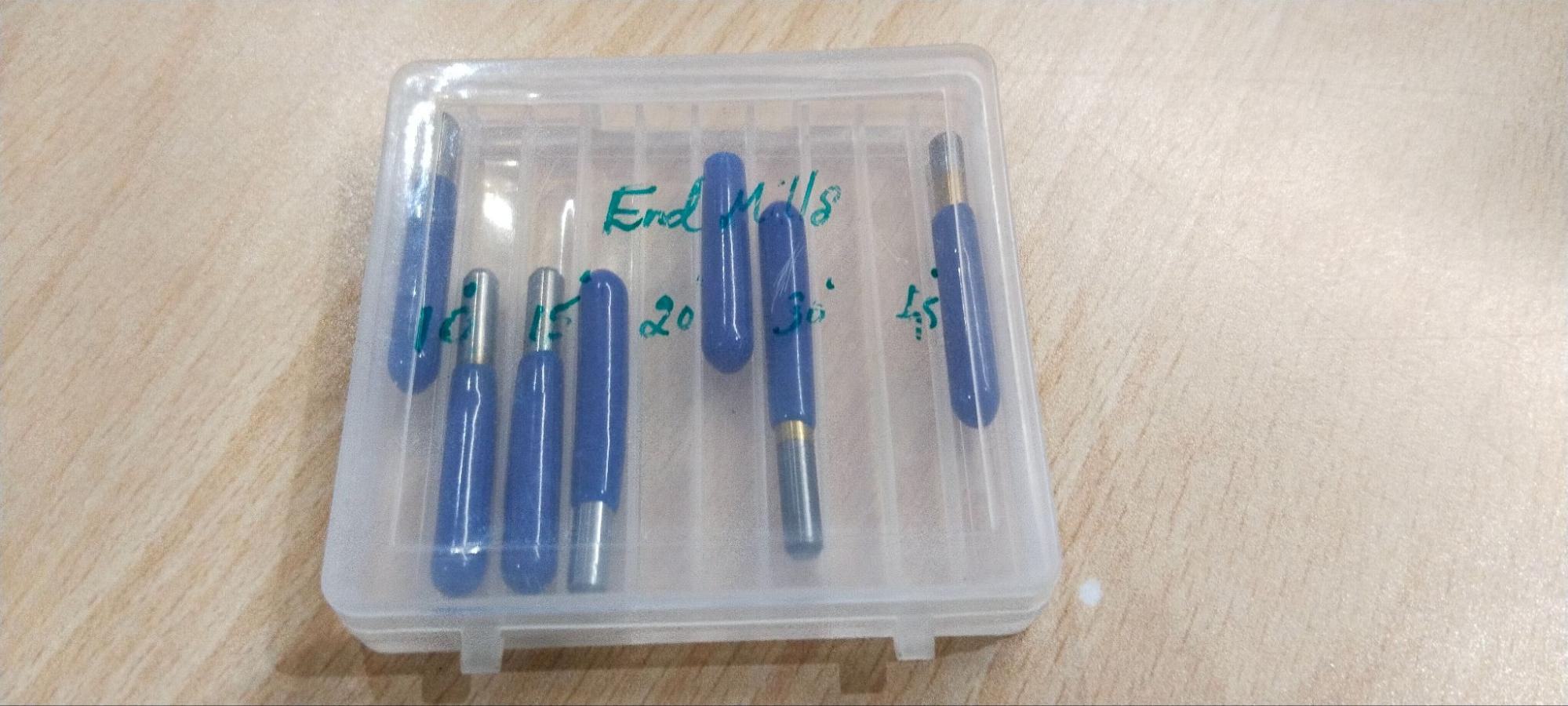
4. Flat End Mill Bits (No specific angle – flat tip, various diameters)
- Main Feature: Flat tip, available in various diameters.
- Application: Cutting PCB shape and removing large copper areas.
- Stage in Process: Used after isolation routing and drilling, as the final shaping process.
- Purpose: Milling straight, flat-bottom paths for board outlines or slots.
- Essential Function: Defines board size or cuts out individual PCBs from a panel.
Basic Conversions
1 mil
- = 0.001 inches
- = 0.0254 millimeters (mm)
1 inch
- = 1,000 mils
- = 25.4 millimeters (mm)
Wegster
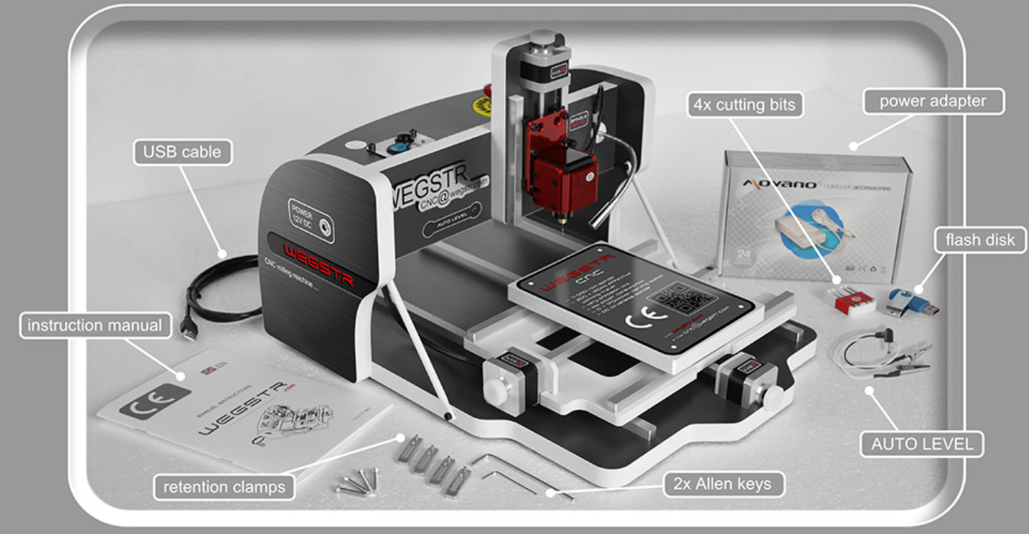
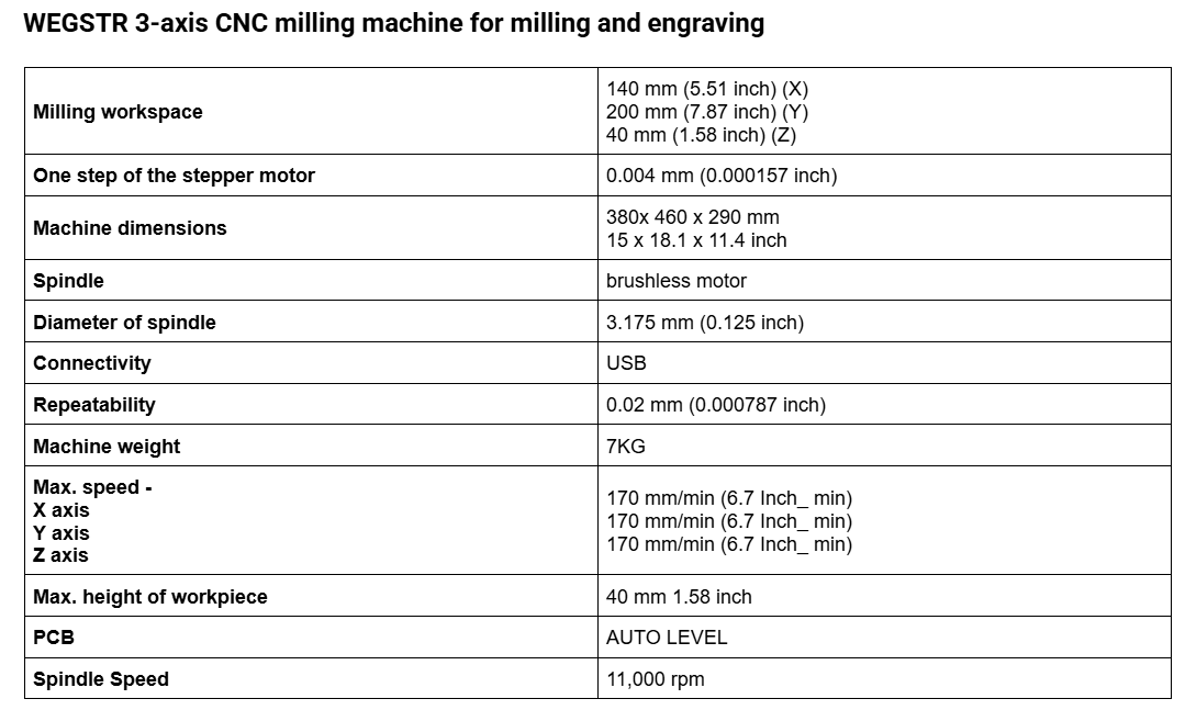
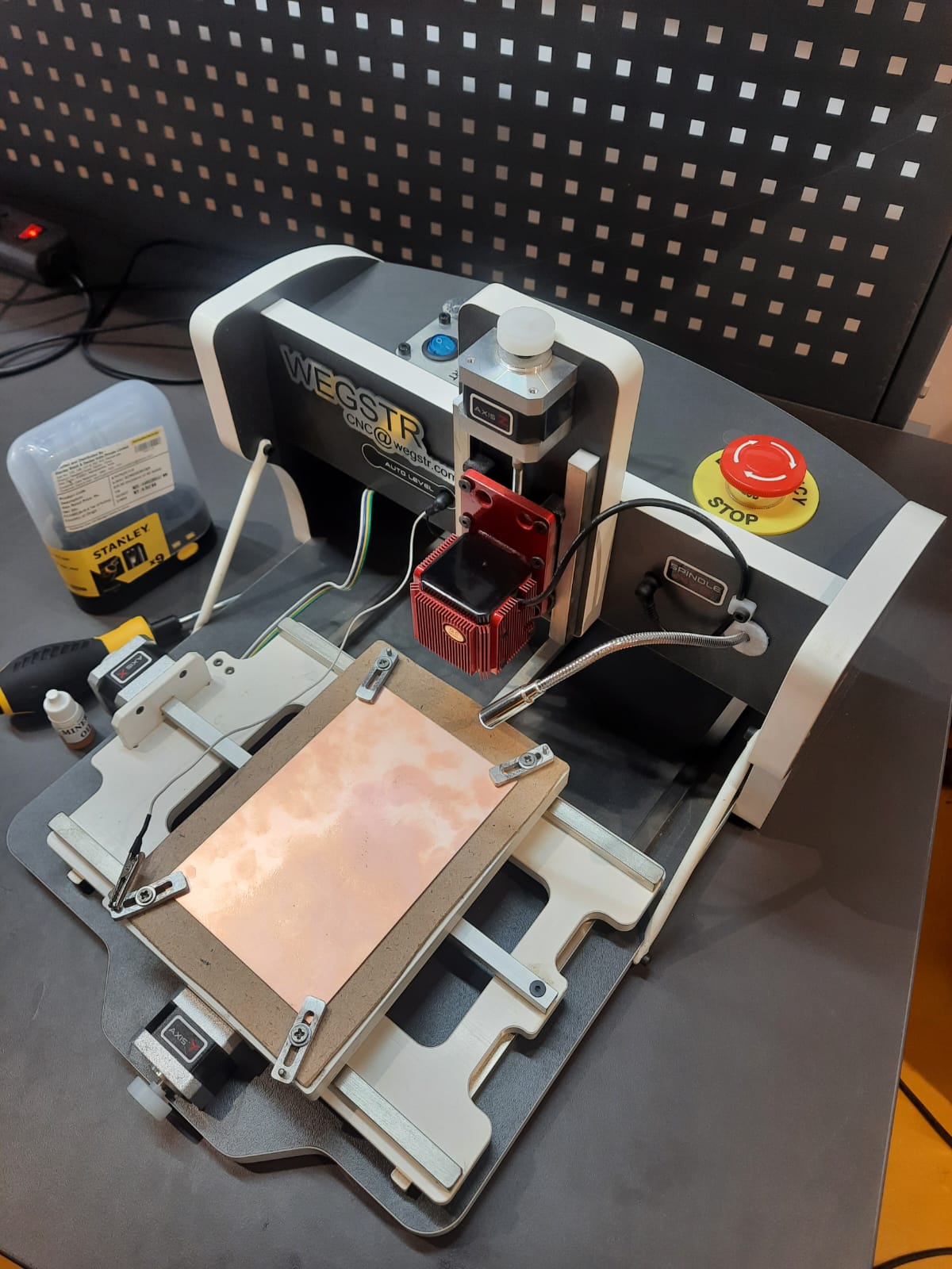
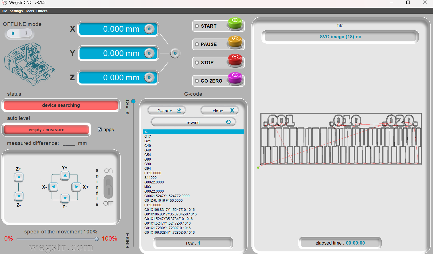
The Wegstr PCB milling machine is a compact desktop CNC designed specifically for rapid PCB prototyping. It allows users to fabricate circuit boards by milling copper-clad boards instead of traditional chemical etching. This is ideal for makers, engineers, and students who want to quickly test their circuit designs. The Wegstr software complements the machine by providing an intuitive interface to load, simulate, and control the CNC toolpaths (usually in G-code format). Users can import files generated from FlatCAM (like the front copper and edge cuts), visualize the milling process, set spindle speeds, and control axis movements with precision. Together, the Wegstr machine and software offer a clean, fast, and eco-friendly approach to producing custom PCBs directly from your digital designs
Machine Details
Setting Up the Wegstr CNC Machine
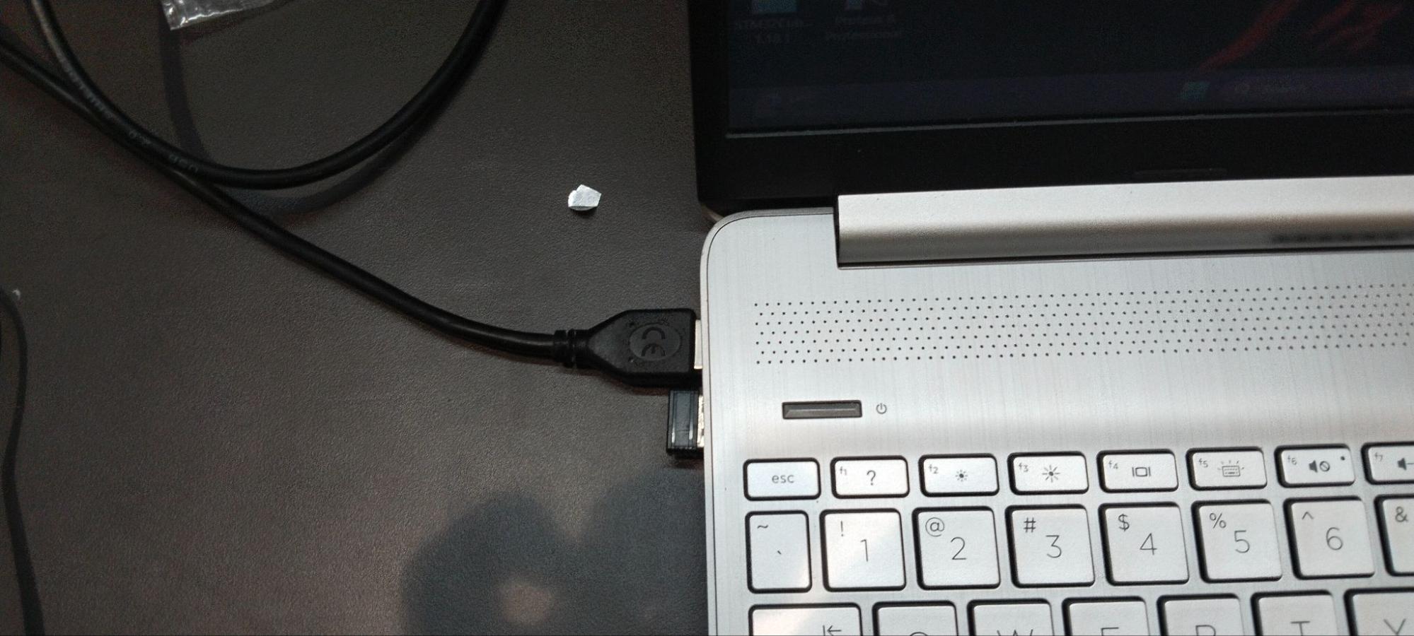
- Connect the Machine via USB
- Use the USB cable to connect the Wegstr CNC machine to your laptop.
- Ensure the cable is securely plugged in and the machine is properly powered on.
- The USB connection allows communication between the machine and your computer.
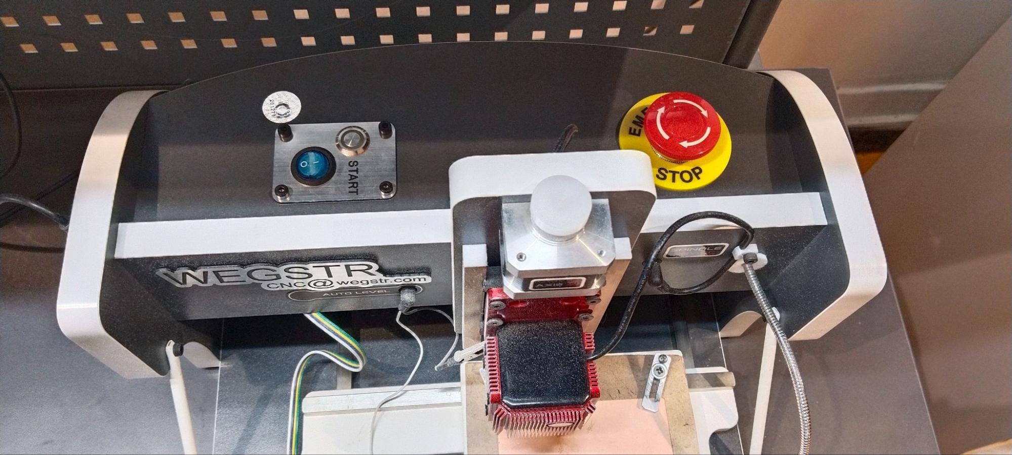
- Locate the power switch on the machine and turn it on.
- The machine will initialize, and indicators may light up to show it is receiving power.
- Wait for the machine to be fully ready before proceeding.
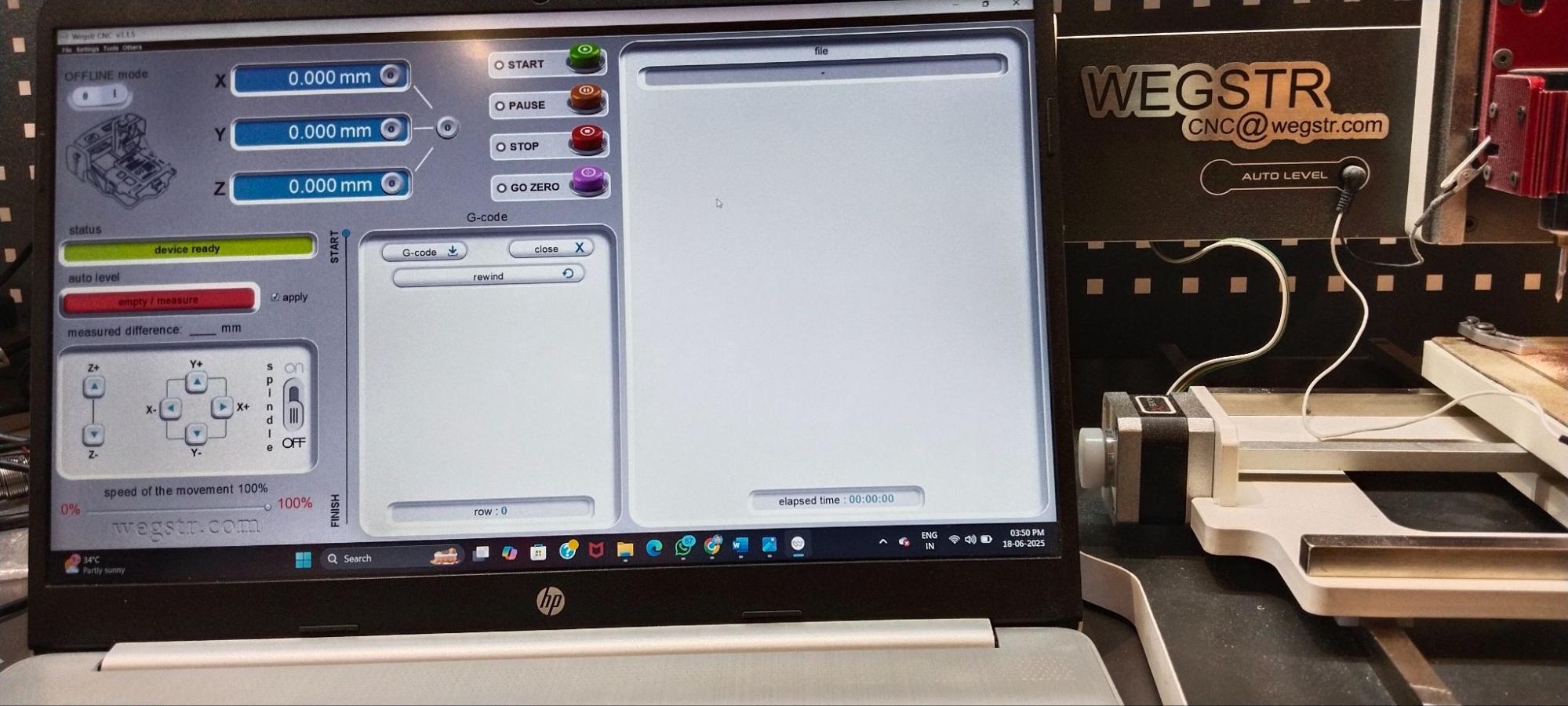
- Open the Wegstr App on Your Laptop
- Launch the Wegstr controlling software or designated app on your laptop.
- The software will search for the device if it is not already connected.
- If not connected, the device searching option will be visible in the software interface.
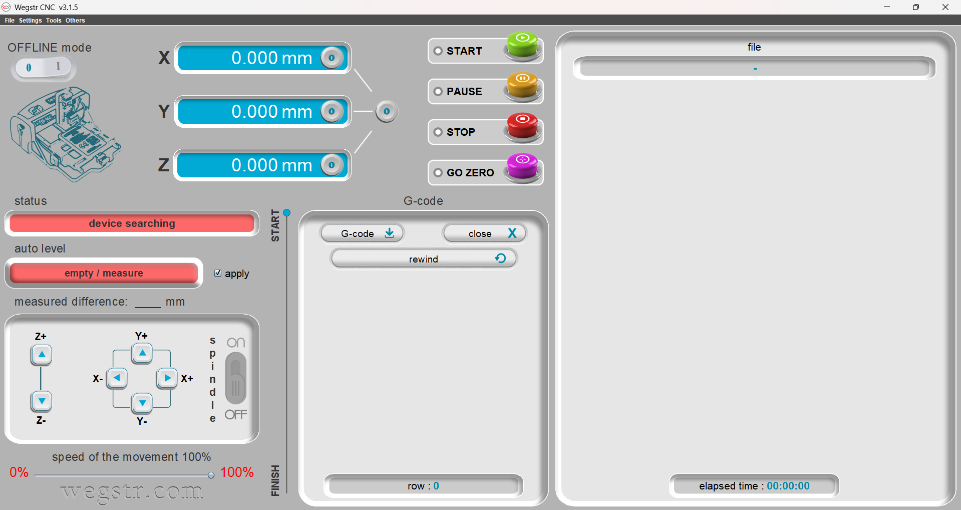
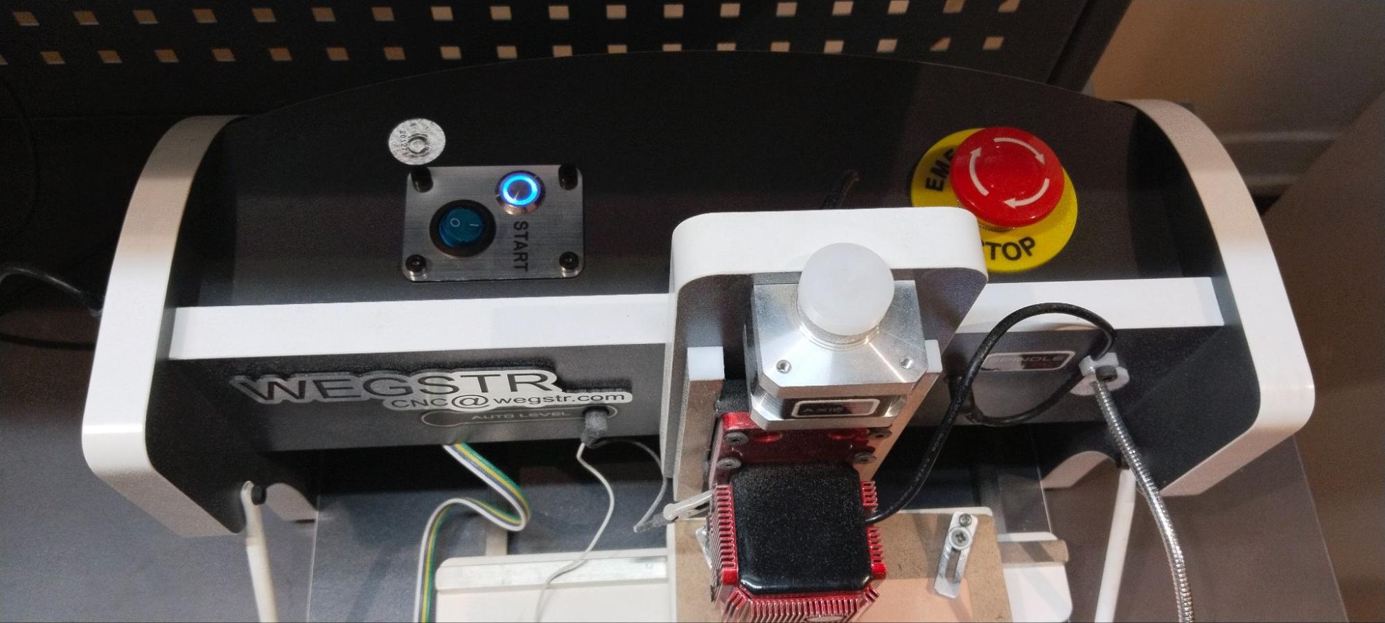
- Device Detection and Connection
- After connecting the USB cable, the software will display a message that the device is released or detected.
- A blue LED on the machine will start blinking, indicating it is ready and connected to the computer.
- The software will now show a live connection status, confirming the machine is ready for use.
- Use the software interface to manually jog the X, Y, and Z axes.
- This allows you to test and calibrate the machine’s movement before starting a job.
- You can also send commands or load G-code files for automated operation.
Milling Traces
- Used for milling wider traces or removing larger areas of copper.
- Suitable for roughing out the board or cutting the main outline.
- Not typically used for fine trace isolation.
- Most commonly used bit in the lab for milling PCB traces.
- Allows for very fine, precise isolation of traces due to its small diameter and sharp tip.
- Ideal for detailed work and separating closely spaced copper traces.
Setting Origin and Auto Level Before Printing
- Prepare the Machine and Board
- Place the PCB board securely on the machine bed.
- Ensure the milling bit is installed and the machine is powered on.
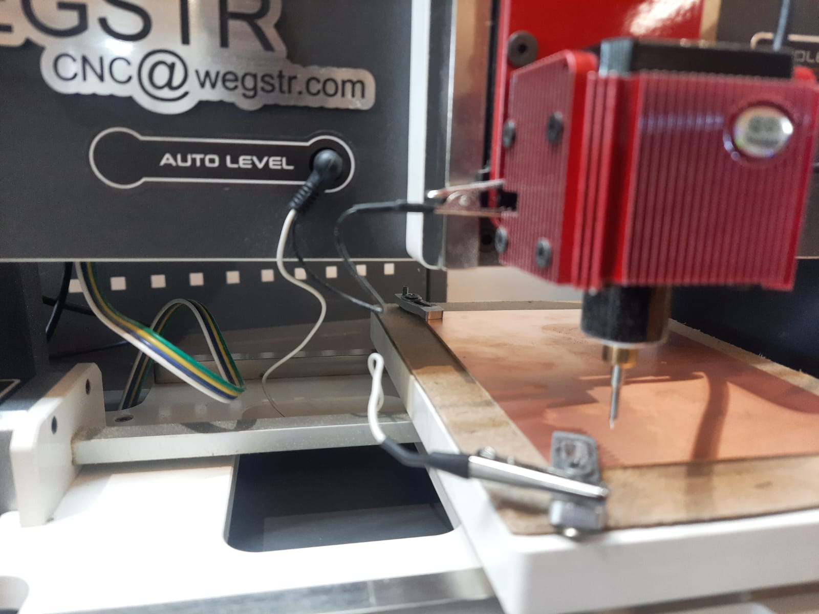
- Check Autolevel with the Bit
- Manually jog the Z axis to bring the bit close to the board surface.
- The machine’s autolevel sensor will detect when the bit touches the board.
- While the bit is not touching the board, the white indicator light remains off. When the bit touches, the light glows to confirm contact.
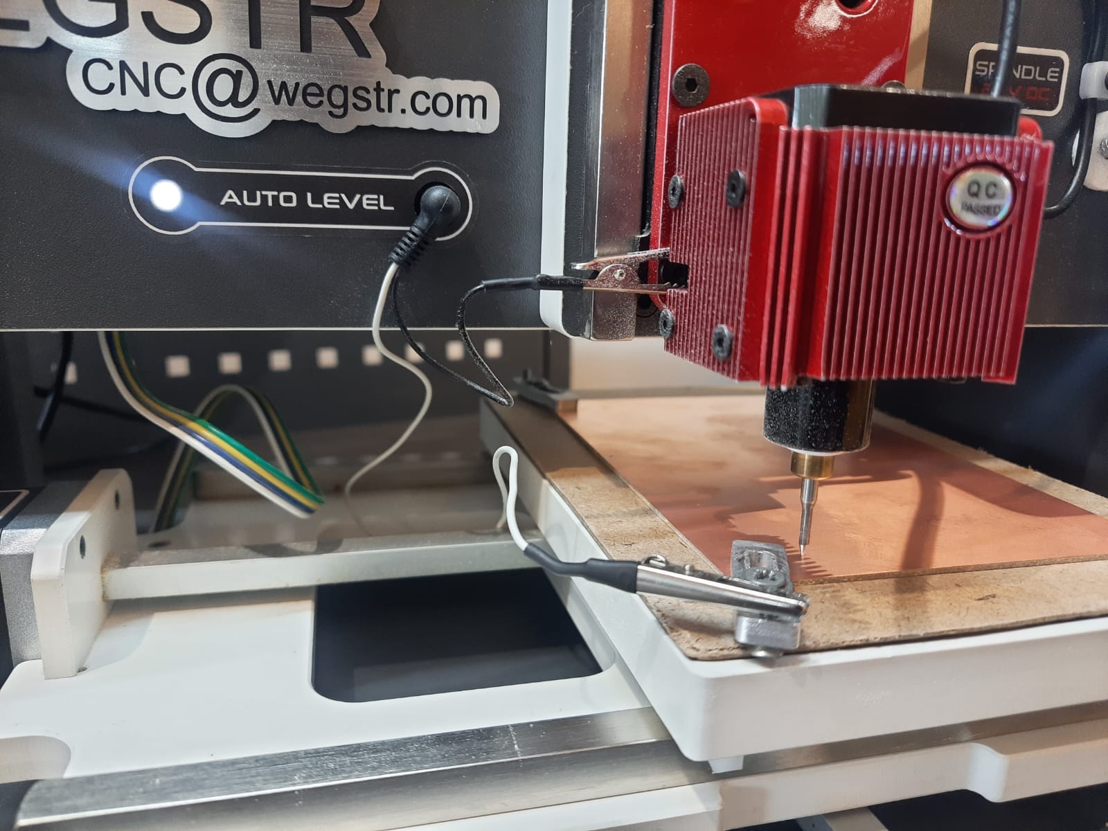
- Set the Origin
- Once the autolevel is verified (bit touches, light glows), press the “0” button in the software to set the origin (home position) for the job.
- Run Autolevel Measurement
- Before starting to print, click the autolevel button in the software interface.
- The machine will automatically measure the height of the board at multiple points covering your entire design area, including all pads and tracks.
- This ensures the milling depth is consistent across the board, compensating for any unevenness in the material.
- Begin the Milling Process
- After autolevel measurement is complete, you are ready to start printing your PCB design.
Exporting and Preparing PCB Design for Milling
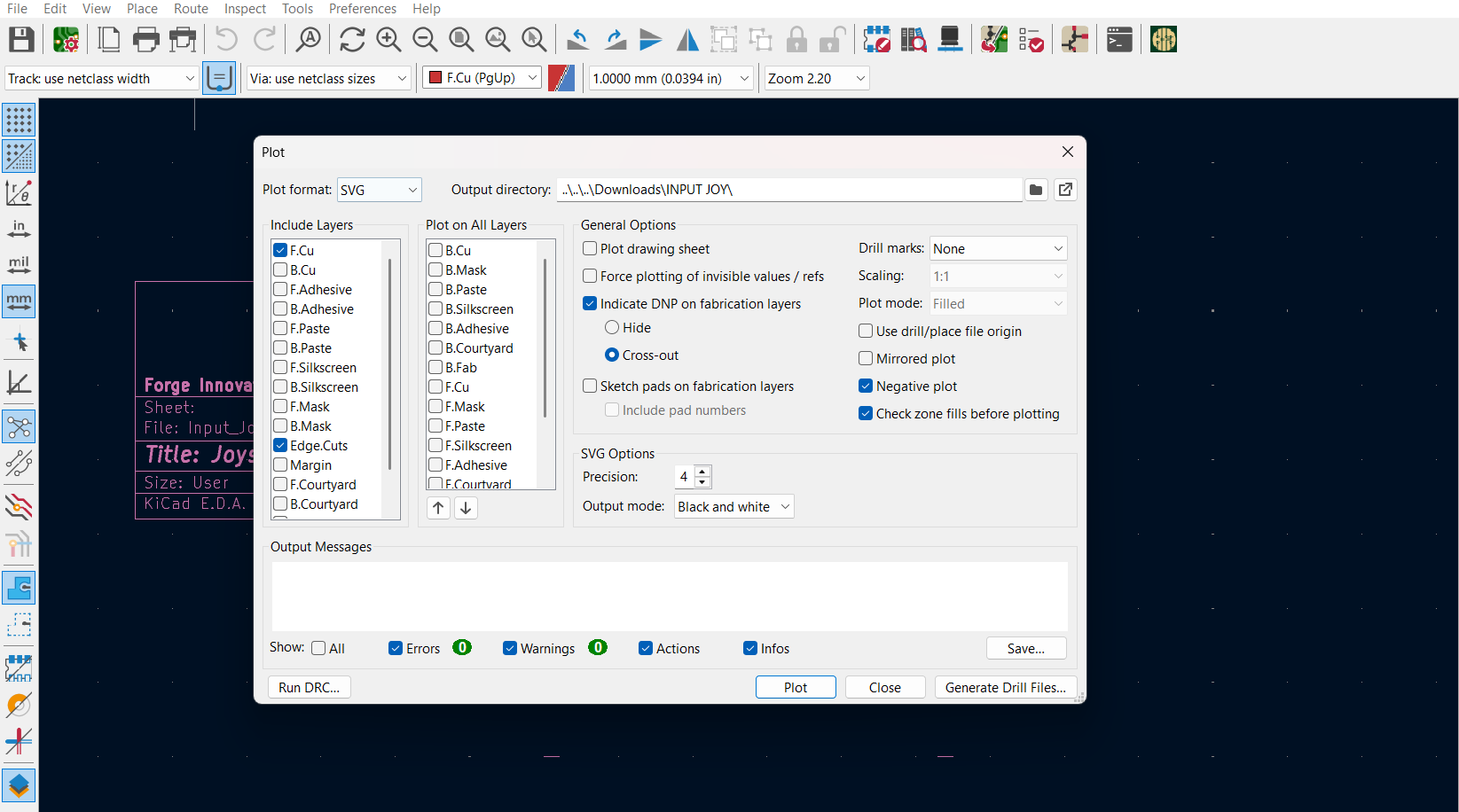
- Export the Front Copper Layer as SVG
- After completing your PCB design in your KIcad tool export the front copper layer as an SVG file.
- In most software, this is done through the menu: File > Export > SVG (or similar).
- Export the Edge Cut (Outline) Layer as SVG
- Similarly, export the edge cut (board outline) layer as a separate SVG file.
- This outlines the shape of your PCB for cutting out the final board.
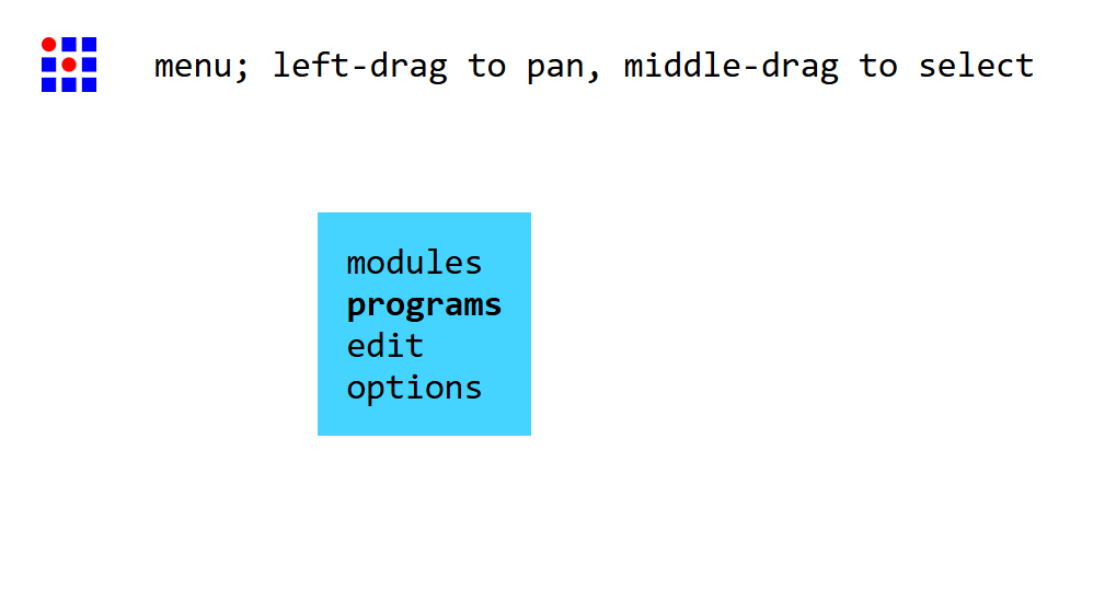
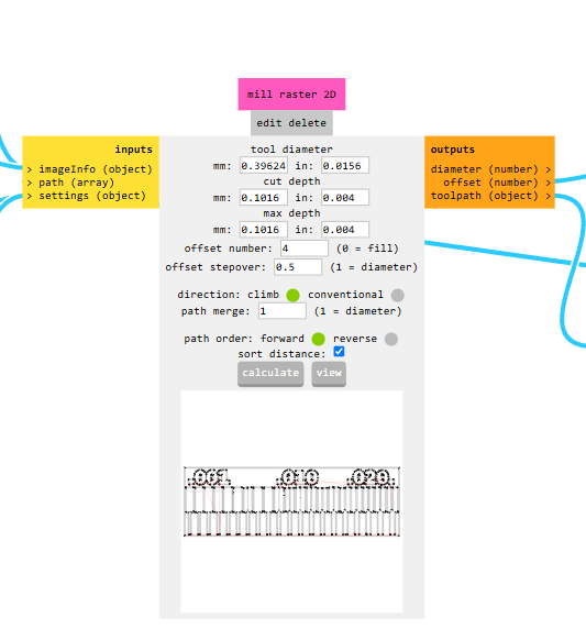
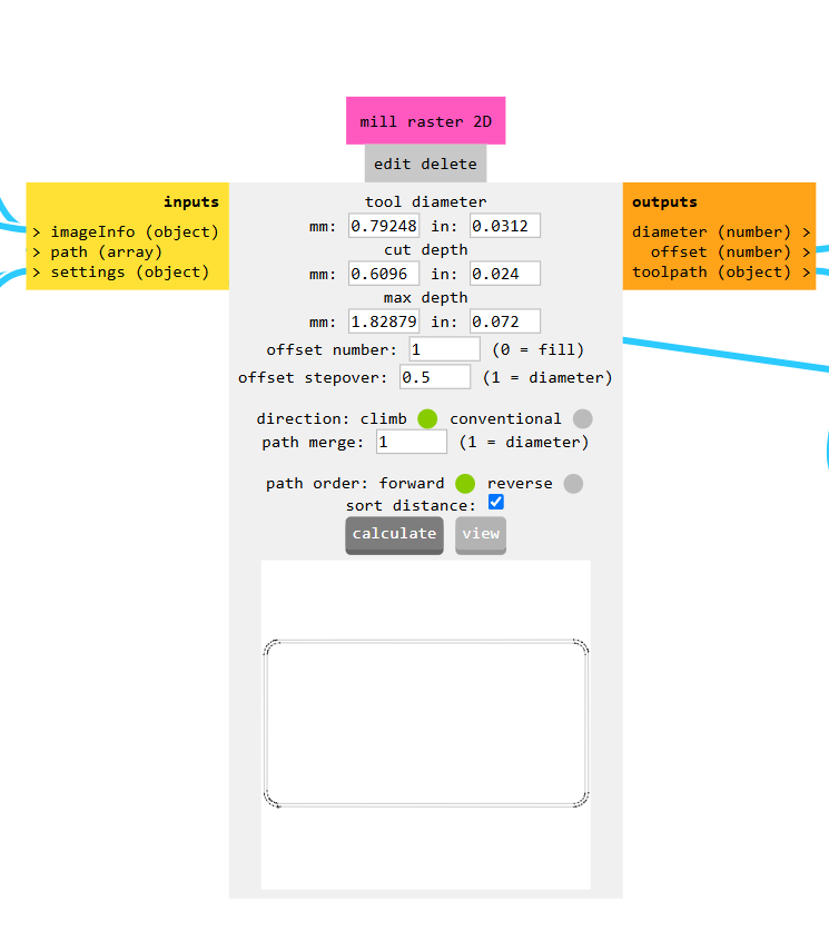
- Open Mods CE Website
- Go to the Mods CE website and open the appropriate workflow for PCB milling.
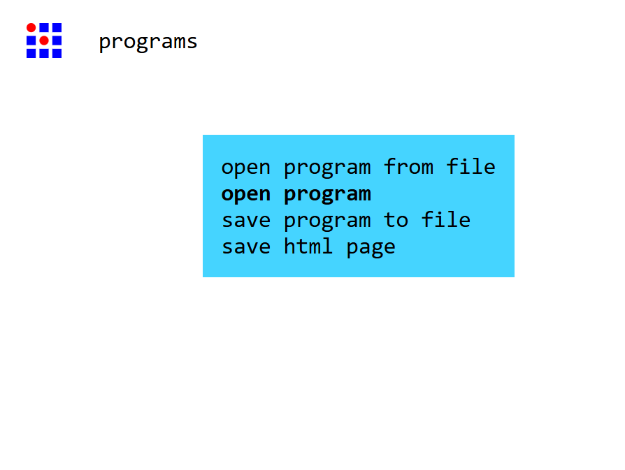
- Load the Front Copper Layer SVG
- Upload the front copper layer SVG file into Mods CE.
- Set the bit angle to 45 degrees and the offset to 10 (units as per your setup, usually mm or mils).
- Click the Send Calculate button to process the file.
- Click Calculate again (or the appropriate button) to generate and download the G-code (NC file) for the front copper layer.
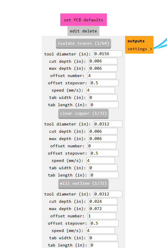
- Repeat for Edge Cut (Outline) Layer
- Upload the edge cut (outline) SVG file into Mods CE.
- For the outline, select the mill outline 1/32 option or choose the appropriate end mill for board cutting.
- Click Send Calculate to process the file.
- Click Calculate to generate and download the G-code (NC file) for the edge cut.
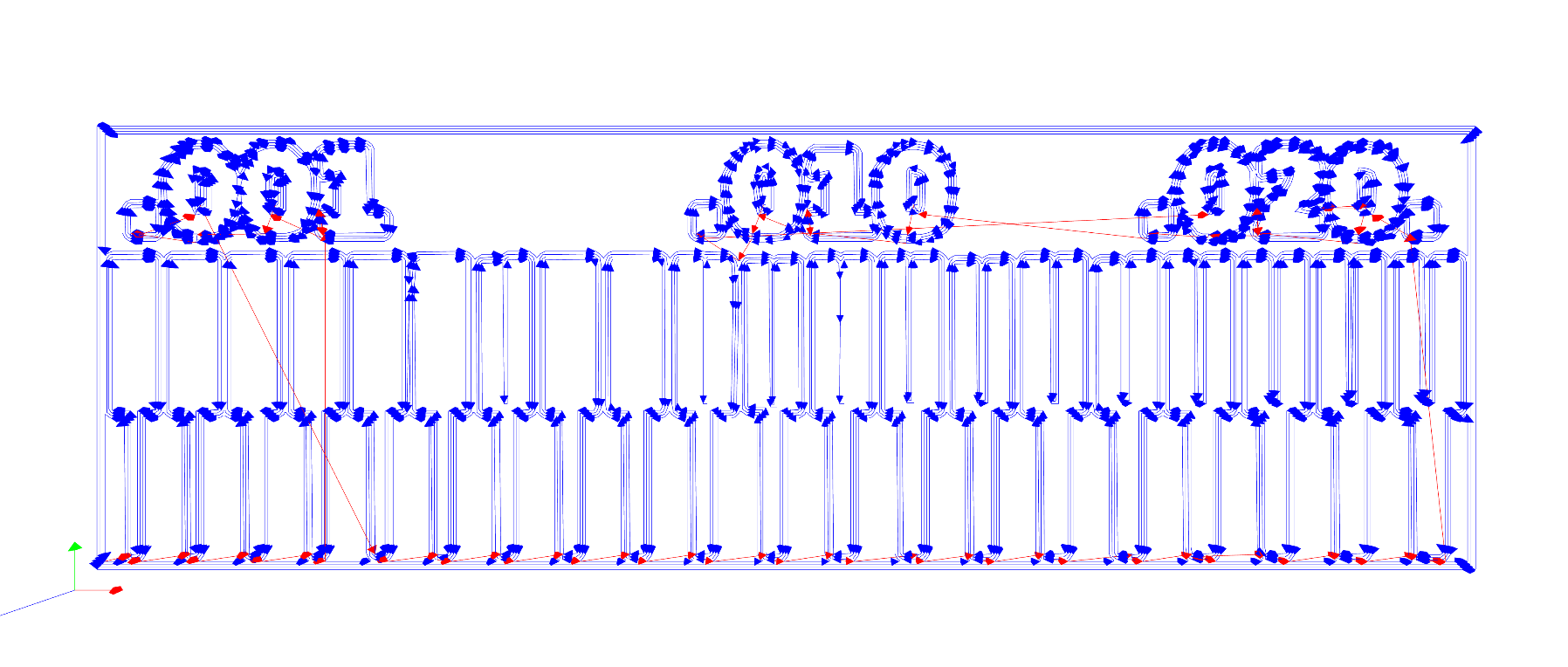
- Ready for Milling
- You now have separate G-code files for milling the copper traces and cutting the board outline.
- Load these files into your CNC machine’s control software to begin milling your PCB.
Final Output
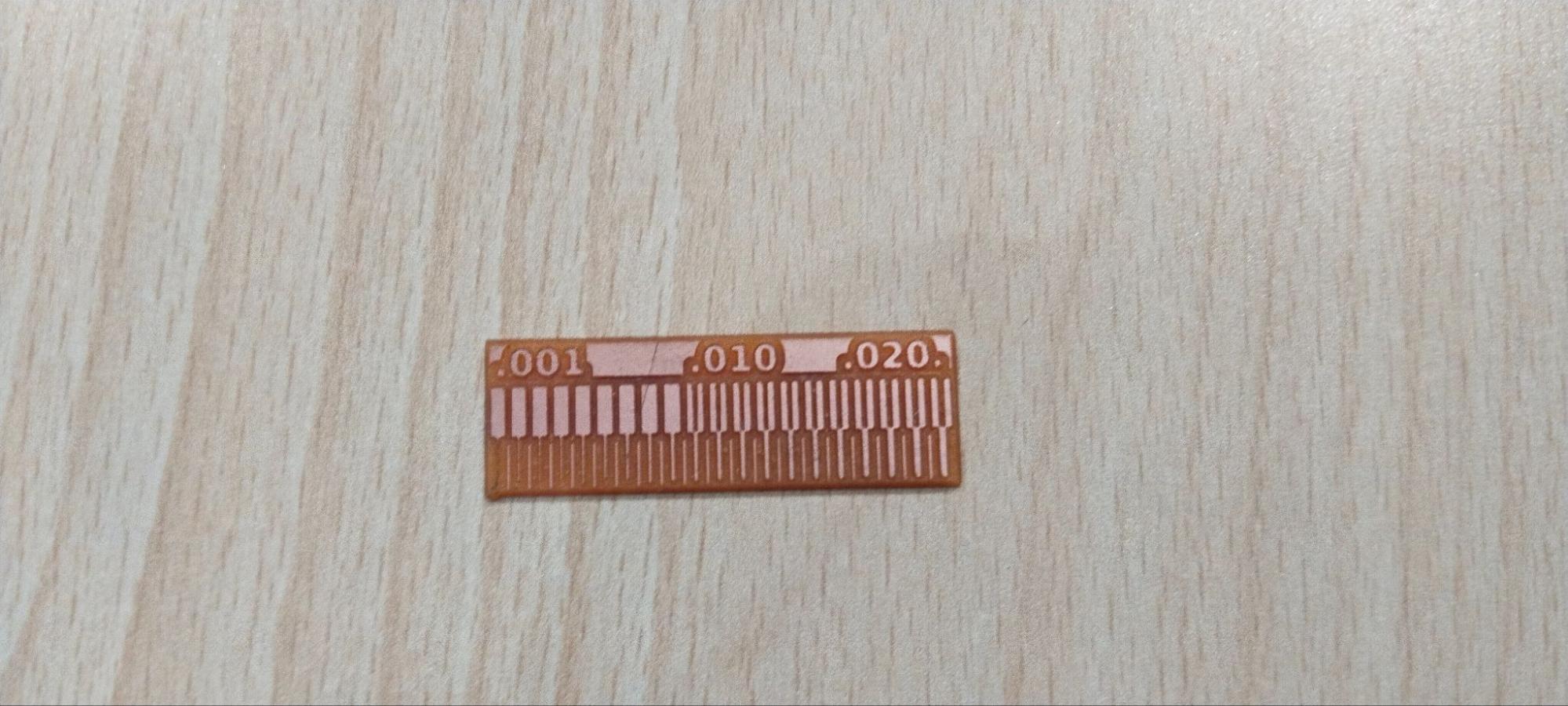
From this test it was clear that the minimum spacing between the traces should be at least 17mils and the traces widths should be a minimum of 10 mills.
<<< Back to Lab Page