Week 6: Electronic Design Assignment
Group Assignment:Use the test equipment available in your lab, such as a multimeter and oscilloscope, to observe and analyze the operation of a microcontroller circuit board.
Document your observations and findings on the group page.
Reflect on what you learned individually on your own page.
Individual Assignment:
Use an EDA tool to design a development board that incorporates parts from the inventory to interact and communicate with an embedded microcontroller.
Group Assignment
We observed the operation of the microcontroller circuit board using various test equipment.
Visit our Group Assignment Page to explore our findings and methodologies.
1. Circuit Design Process
Overview of the Process
The circuit design process involves defining objectives, creating a block diagram, designing detailed schematics with tools like KiCad, running simulations, and converting designs into PCB layouts. Finally, prototypes are built and tested, ensuring functionality, safety, and performance through a structured, error-minimizing approach.
Using Ki Cad to build and simulate the circuitKiCad is an open-source and free tool for Electronic Design Automation (EDA) that enables the creation of electronic circuits and PCB designs. With features like schematic capture, PCB layout, 3D modeling, and Gerber file generation, it is widely used by both engineers and hobbyists to bring hardware concepts to life.
Open your web browser and search for "KiCad" on Google.
Click on the official KiCad website link, which is www.kicad.org.

On the KiCad website, click the Download button.

Choose the operating system you want to install KiCad on. Since I’m using Windows, I will select Windows.

You can select the latest version to download, but I prefer to install a specific older version of KiCad because it includes a feature that was discontinued in later versions. To do this, click on the Previous Releases link.
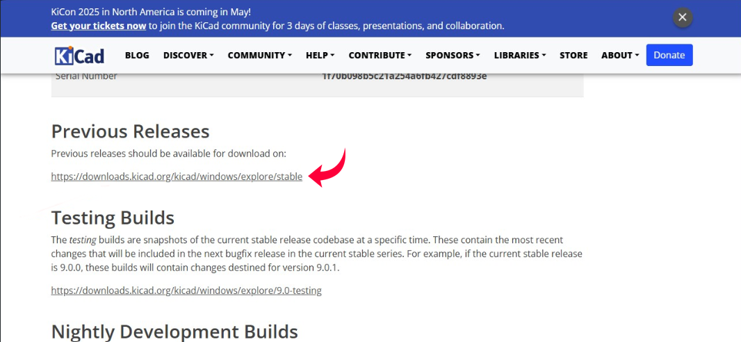
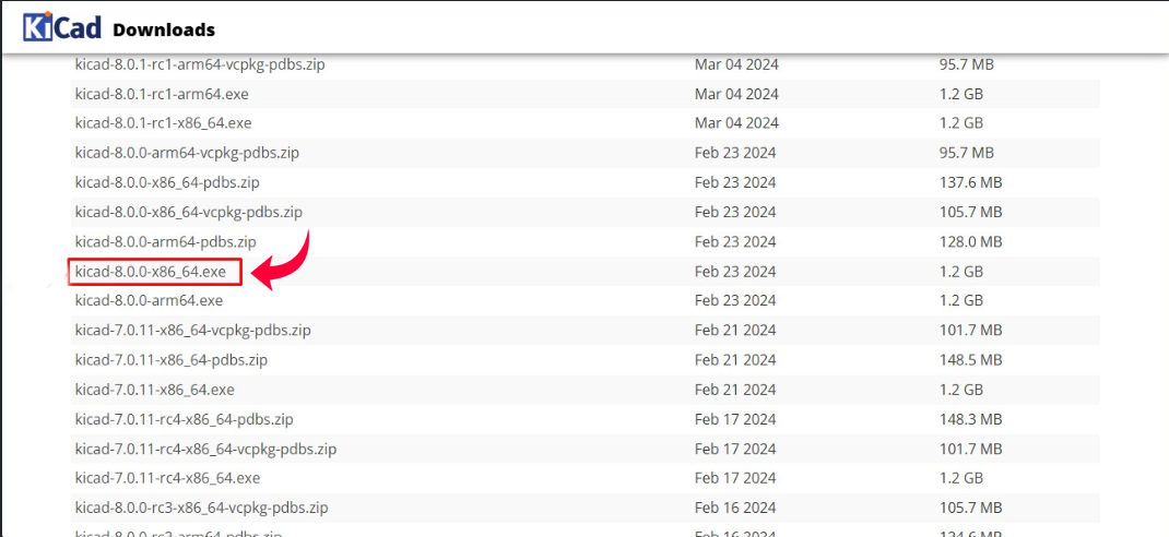
From the list of previous versions, click on Kicad-8.0.0 x84x64.exe. This version, and earlier ones, include a feature that allows PCB designs to be downloaded in SVG format. This format is particularly convenient for use with an online tool called ModsProject, which is used for milling designs.
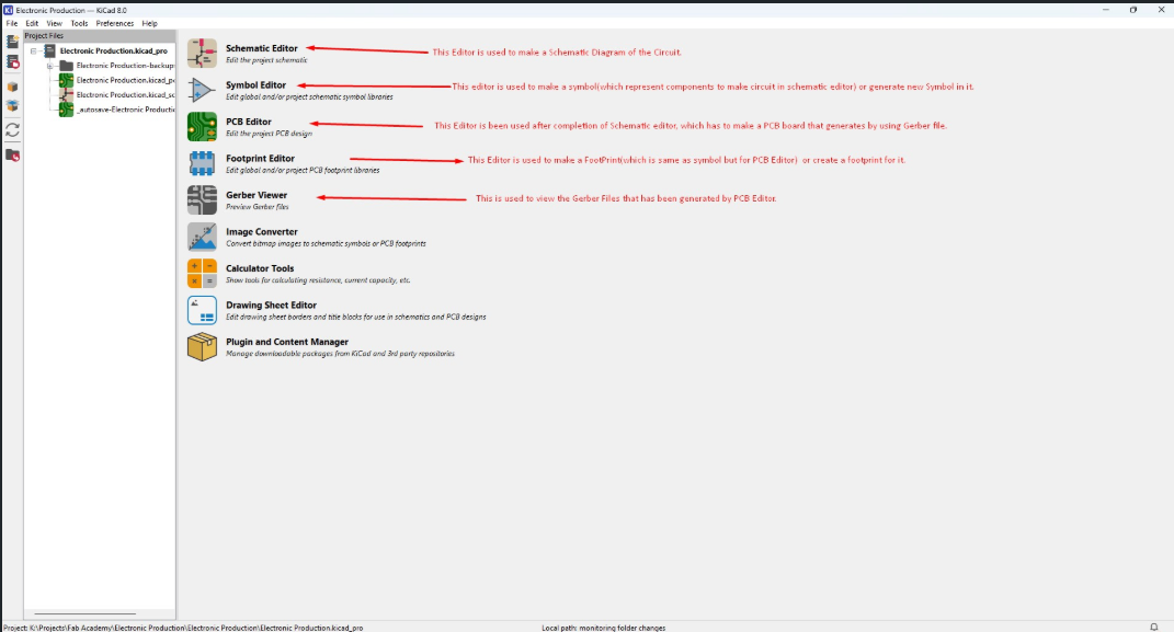
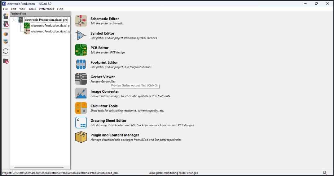
When you open the KiCad software, the main window will appear, containing the following tools: Schematic Editor, Symbol Editor, PCB Editor, Footprint Editor, and Gerber Viewer.
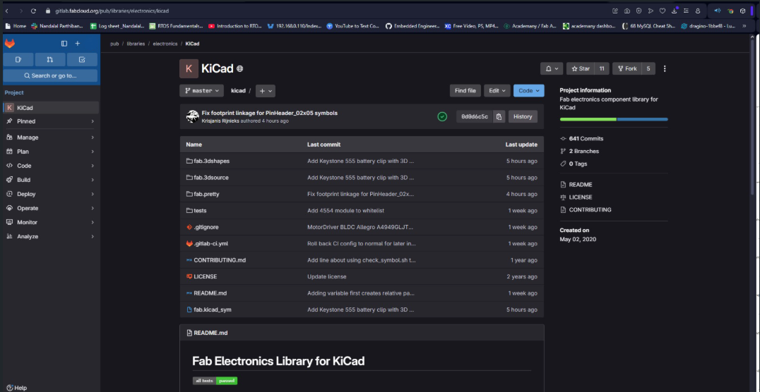
Open Google and search for Fab KiCad Library.
Look for a link to fabcloud.org in the search results and click on it to access the library download page.

On the fabcloud.org page, you may notice a layout similar to GitLab. To download the library:
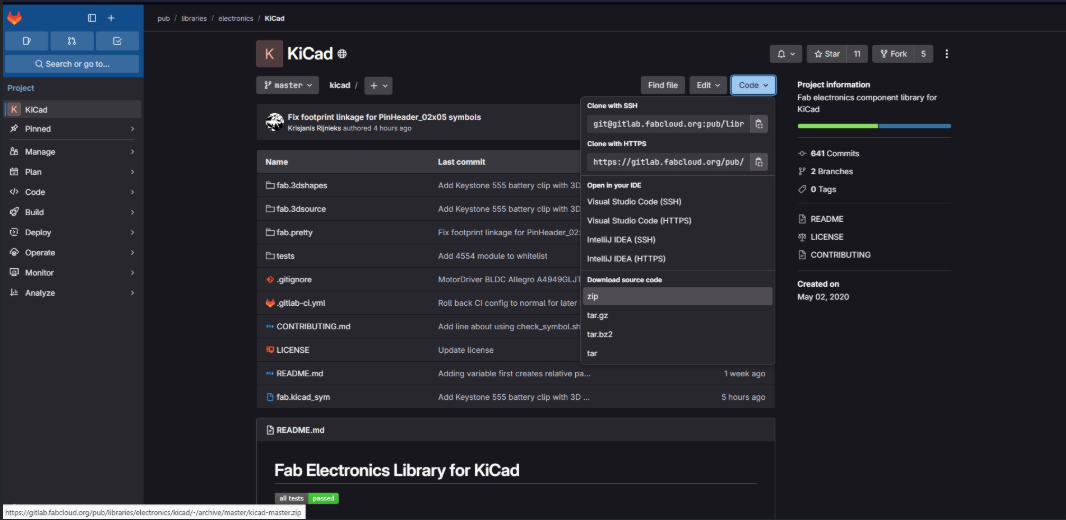
Locate and click on the CODE button.
Choose the appropriate option to download all the files (e.g., Download ZIP).
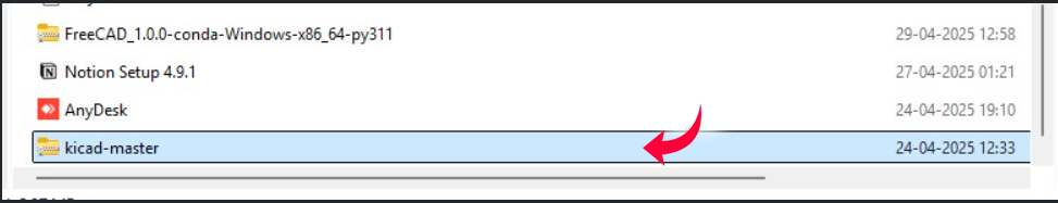
After downloading the file:
Locate the downloaded file on your system.
Right-click on the file and select Extract All or use your preferred extraction tool.
Choose a destination folder that you can easily remember for later use.
In the KiCad main window:
Click on Preferences in the menu bar.
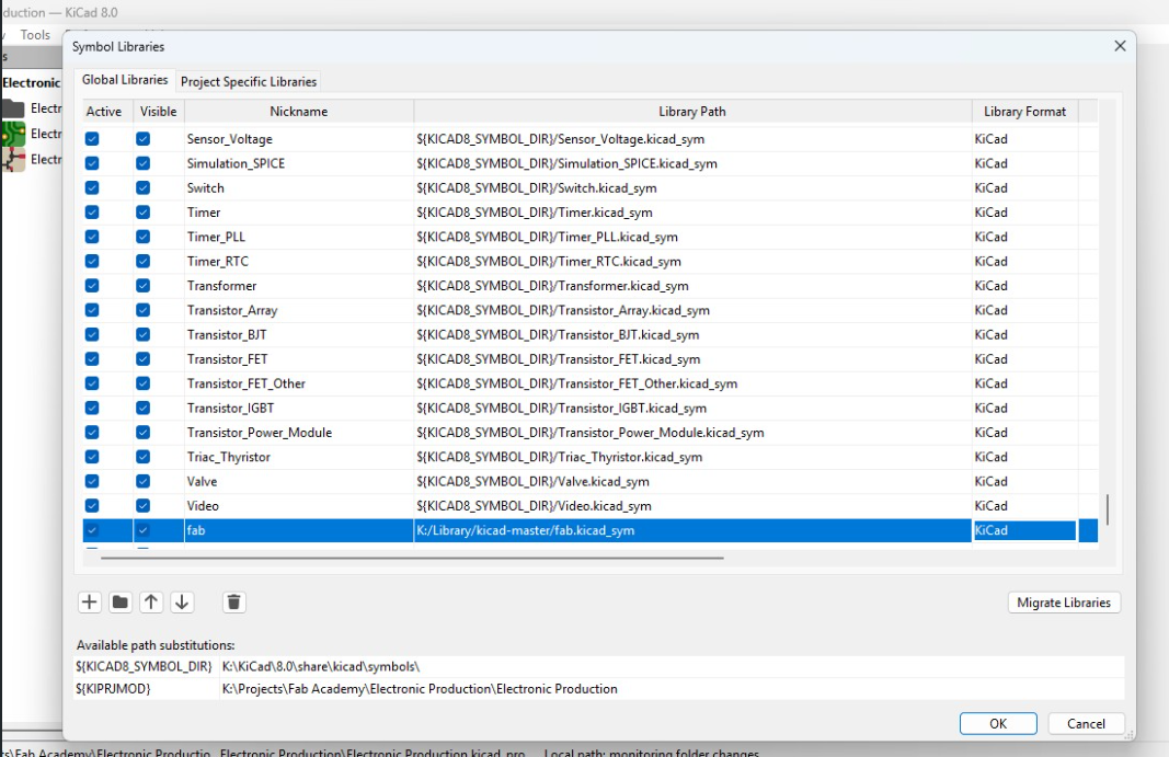
Select Manage Symbol Libraries from the dropdown menu and click on it.
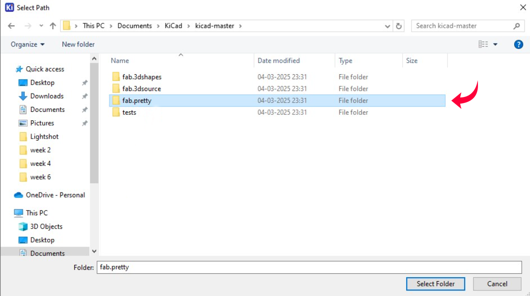
In the Manage Symbol Libraries window, click on the New Folder button.
This action will open a new window where you can specify the folder location.
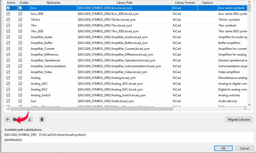
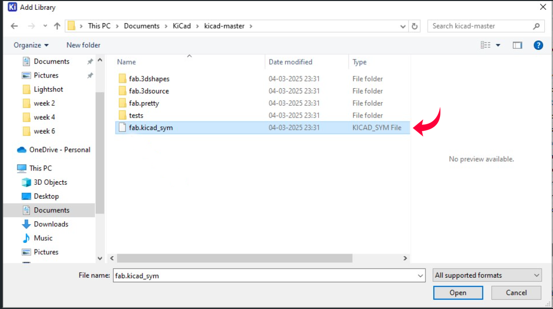
Navigate to the extracted "Kicad-master" folder, select the fab.kicad_sym file, and upload it into the Symbol Editor.
After importing the file, you’ll see a confirmation that it’s been successfully added and it will be visible in the Symbol Editor.
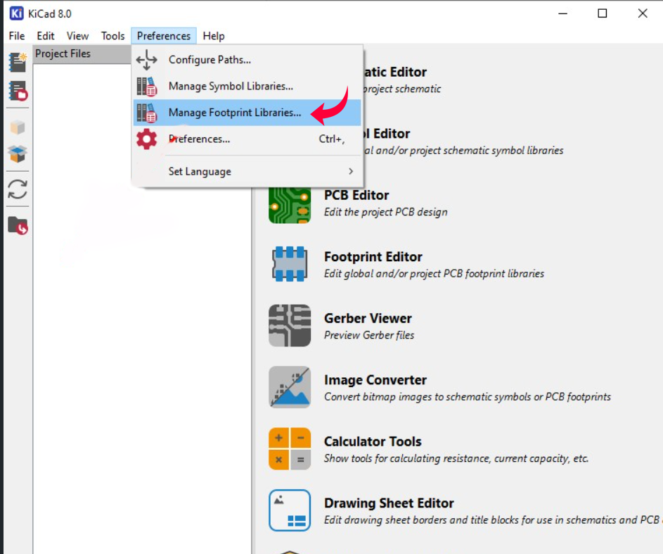
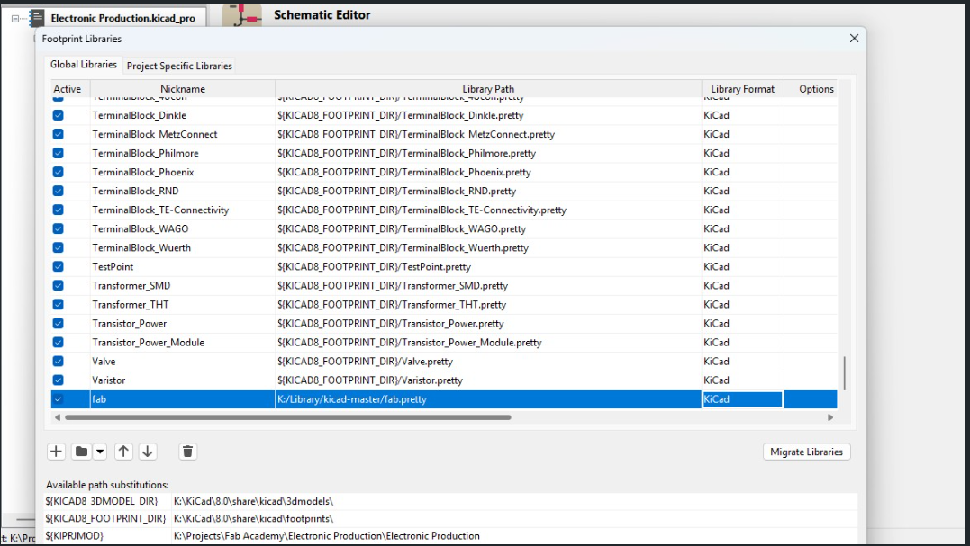
Now, return to the KiCad main window and navigate to Preferences → Manage Footprint Libraries.
A window similar to the Symbol Editor will open, but here you will add footprint data. Click the Add (+) button, then enter the name Nickmake (which should match the name used in the Symbol Editor when adding the new symbol).
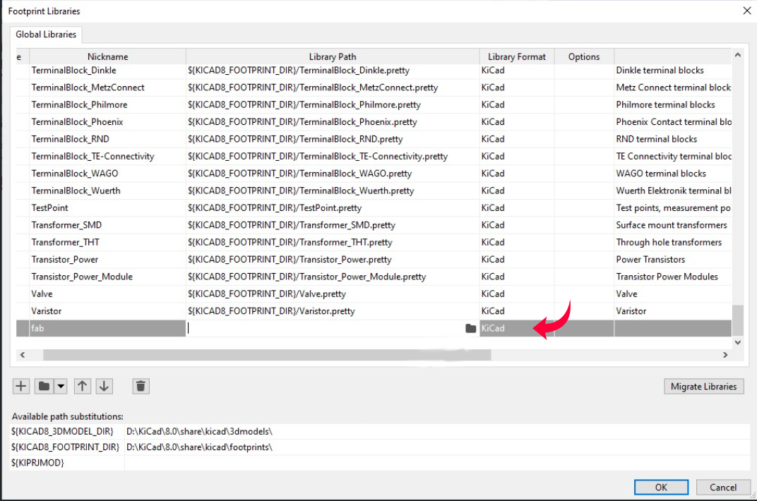
Navigate to the extracted "Kicad-master" folder and select the fab.pretty folder to upload it into the Footprint Editor.
After importing the file, you’ll receive confirmation that it has been successfully uploaded, and it will be visibly listed.
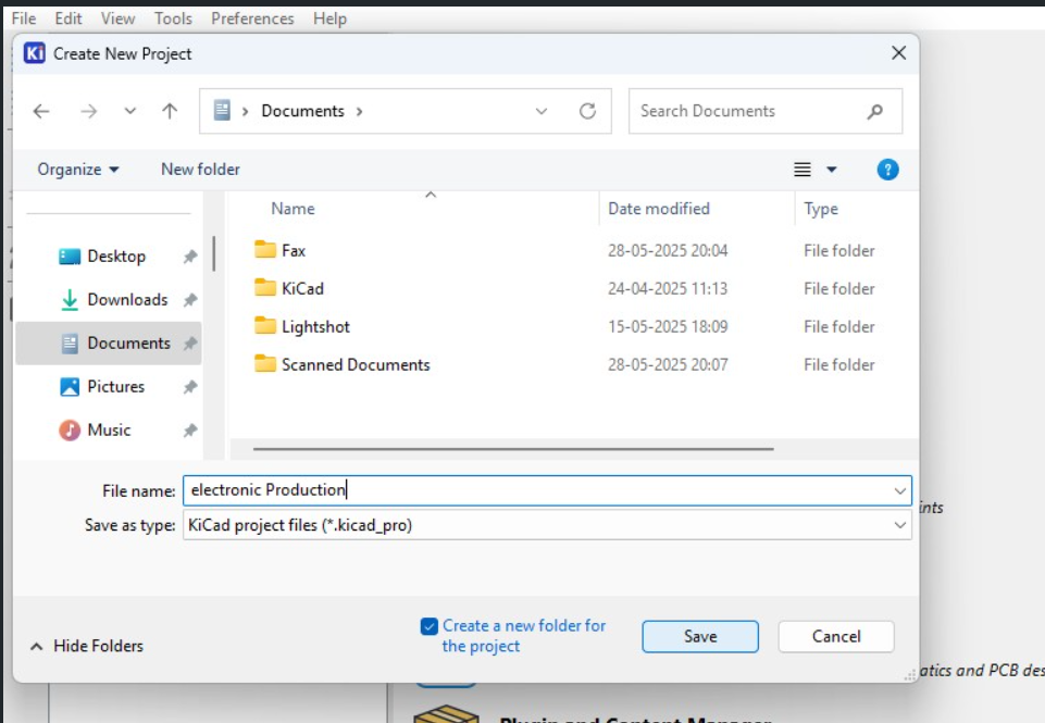
Open KiCad, and when the main window appears, go to File → New Project.

Browse to your desired location and name the project— in my case, I named it "electronic Production".
You will see two files created:
Schematic File (.sch)
PCB Layout File (.kicad_pcb)
2. Component Selection
Component Selection
Component selection is essential in electronics design, affecting functionality, performance, and cost. Start by defining requirements such as voltage, current, and size, and select core components like microcontrollers. Identify supporting components like resistors and capacitors, ensuring compatibility and adherence to electrical specifications.
After opening the KiCad project file, evaluate components based on size, packaging, availability, and cost. Use datasheets and simulations to ensure seamless compatibility, reliability, and compliance for critical applications. Thoughtful selection leads to efficient, cost-effective designs that streamline prototyping and meet performance goals.
To make the schematics choose the components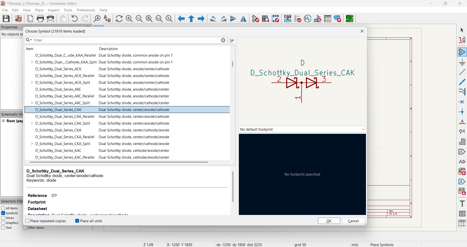
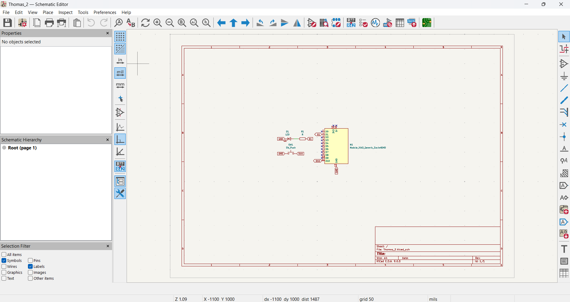
After choosing the components along with the footprint make the schematics
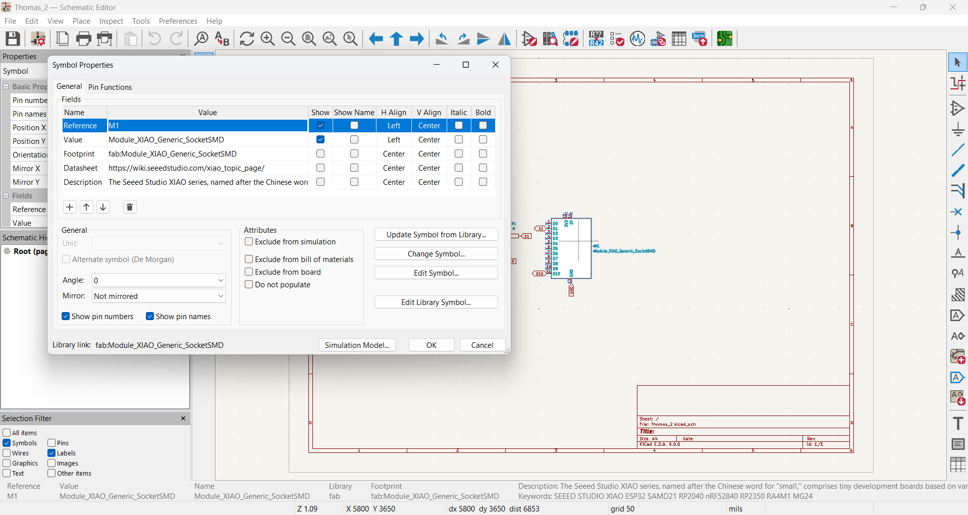
you can edit the properties of the components using this dialog box
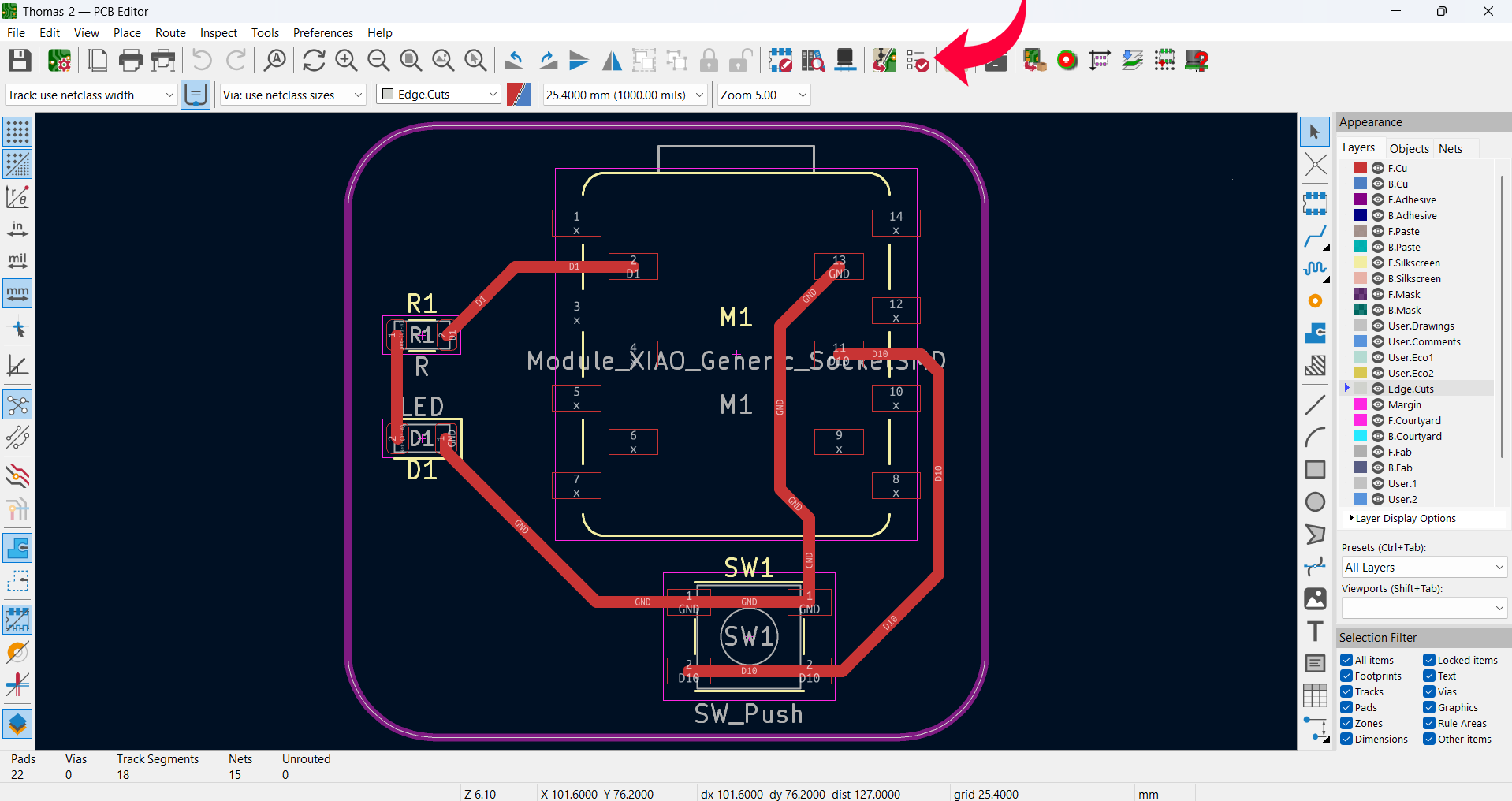
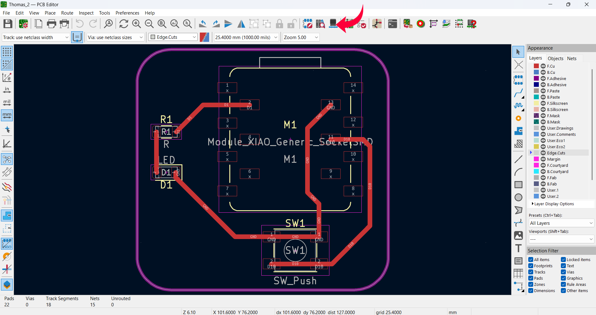
Now move on to the PCB editor
3. Circuit Simulation
Circuit Simulation
Using KiCad, circuit simulation involves designing schematics, configuring analysis parameters like DC or transient, and running simulations to analyze performance. Outputs such as waveforms are reviewed to identify issues, refine designs, and ensure reliability before prototyping. KiCad streamlines the process, saving time and enhancing efficiency.

Following steps are done to get the DRC Check:
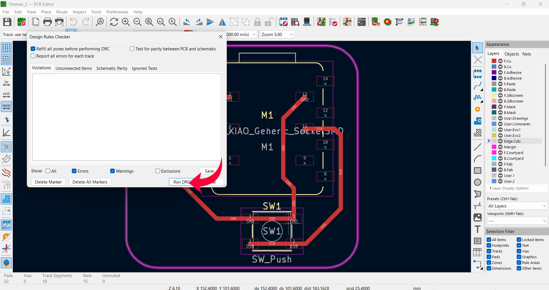
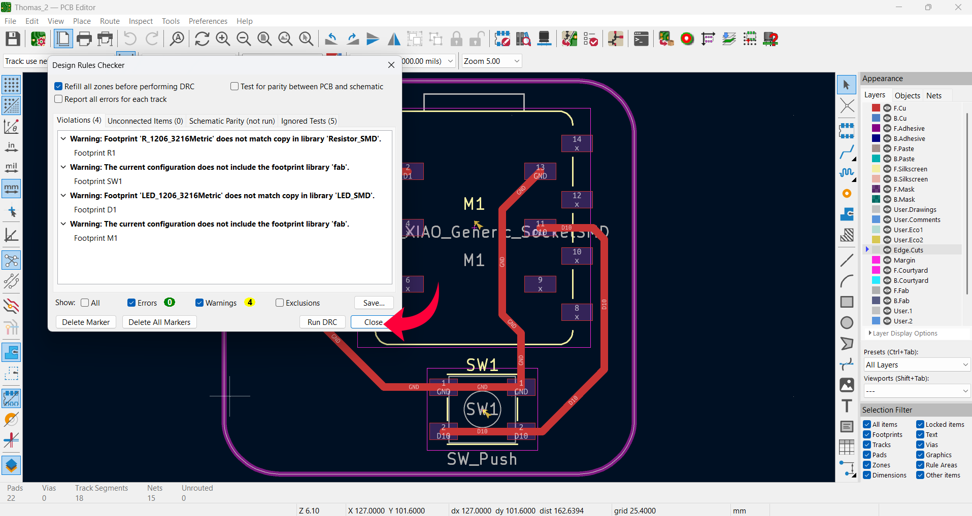
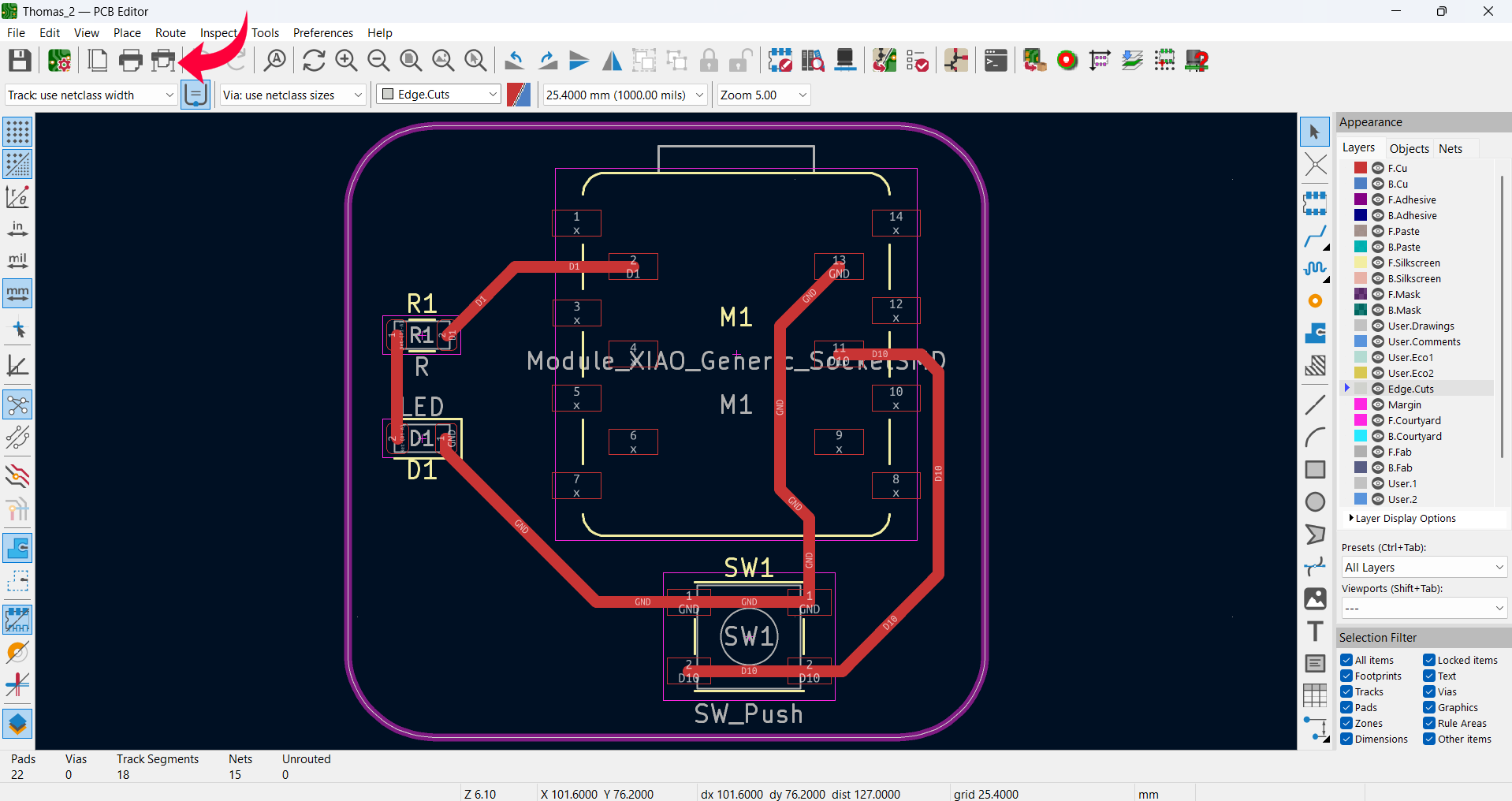
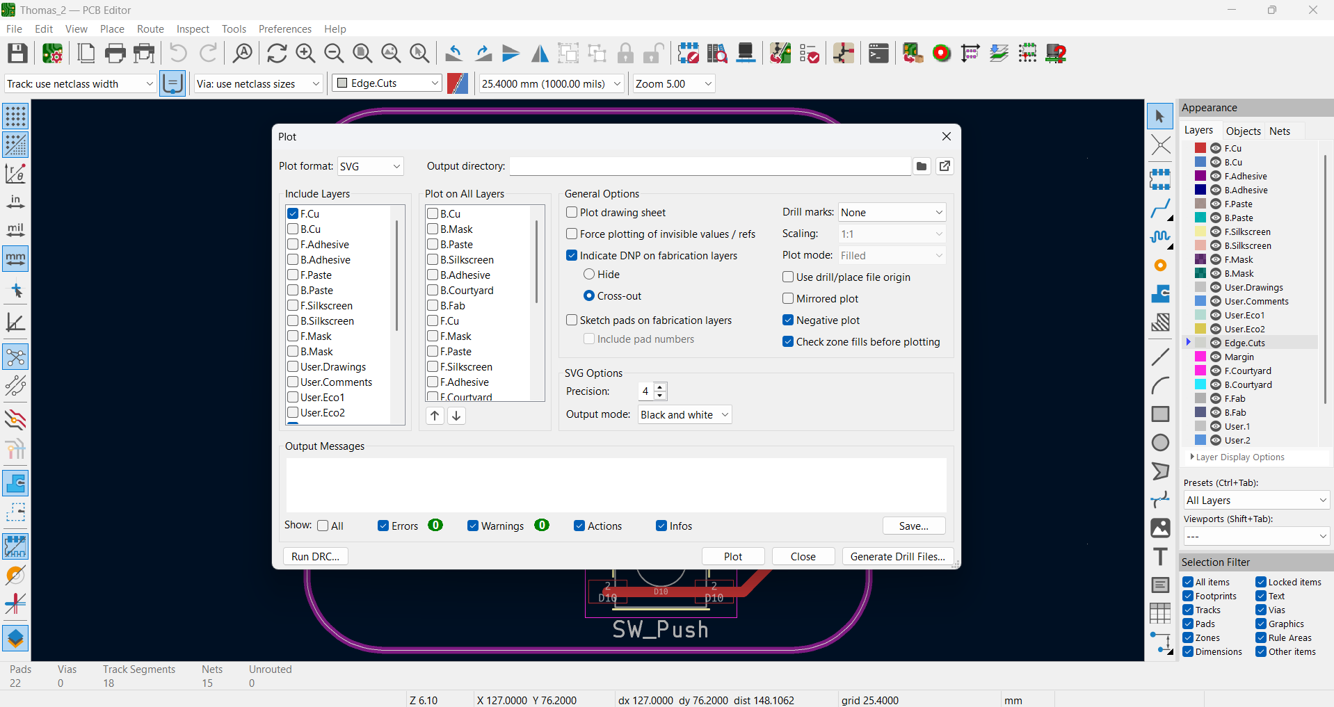
Once the Drc Chec k is over export the files in SVG format to make the PCB follow the steps below:
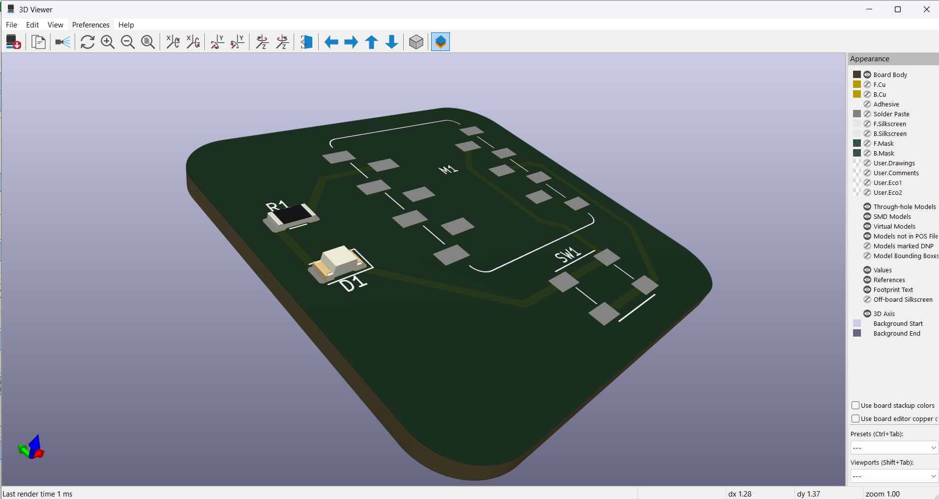
Heroshot of the Board:
Files for downlaod: