Electronics Design
- Use the test equipment in your lab to observe the operation of a microcontroller circuit board (as a minimum, you should demonstrate the use of a multimeter and oscilloscope)
- Document your work on the group work page and reflect what you learned on your individual page
- Use an EDA tool to design a development board that uses parts from the inventory to interact and communicate with an embedded microcontroller
#.Group assignment:
Group Work Reflection
In the lab, our group worked together to observe and verify the operation of a microcontroller circuit board using standard test equipment. We started by using a digital multimeter to check the power supply, ensuring the board was receiving the correct voltage at key points like Vcc and GND. We also measured continuity and resistance across various components to confirm proper connections and detect any faults. Then, using an oscilloscope, we examined signal waveforms on selected digital I/O pins, which allowed us to visualize pulse signals and confirm the timing and logic levels of outputs such as PWM signals and clock pulses. This collaborative testing process helped us better understand the circuit’s real-time behavior and confirmed that the microcontroller was operating correctly.
Here is the Group assignment(link)
#.Individual assignment
In this project, the goal was to design a development board using an EDA tool that integrates components from our inventory to interact with an embedded microcontroller. The final output would be a functional circuit board that can perform tasks like blinking LEDs or interfacing with peripherals, forming a bridge between hardware design and embedded programming.
My Approach
I began with two ideas in mind. First was to use the Seeed Studio XIAO ESP32C3 from week 4, where I had already successfully programmed it to blink three LEDs in Wokwi. I planned to replicate that design in KiCad.
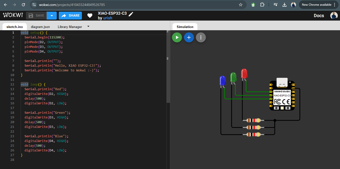
In Wokwi, I used the Seeed Studio XIAO ESP32C3 to blink three LEDs by connecting them to GPIO pins and programming them to turn on and off in sequence.
The second idea, which aligns with the upcoming electronics production week (week 8), was to use the XIAO-RP2040 module and design a custom board around it.For both approaches, KiCad was my primary tool of choice due to its robust features for schematic design and PCB layout.
XIAO-RP2040 pinout
The Journey: Challenges and Decisions
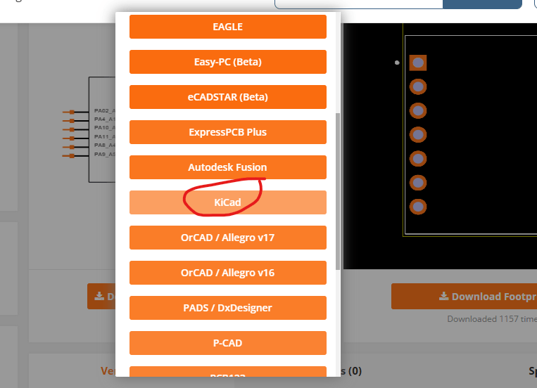
Since this was my first time using KiCad, I wanted to explore it thoroughly and learn how to find and import component symbols and footprints. I started by searching for the XIAO ESP32C3 symbol and footprint on SnapEDA , where I found them, downloaded them, and imported them into KiCad.
.png)
Downloading the footprints and symbols supported by kicad
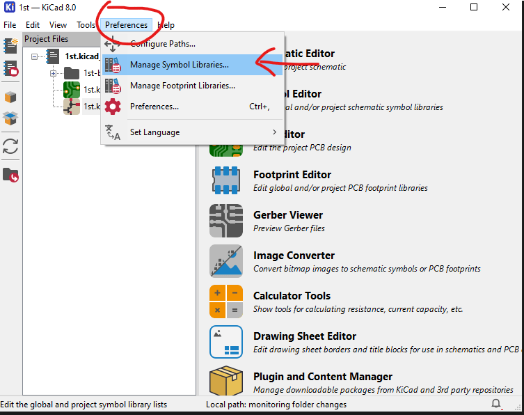
Installing the symbols in kicad
I then created the schematic using the circuit I had built in Wokwi in week 4, which was a bit challenging at first but rewarding. After completing the schematic, I moved on to the PCB editor and began tracing the board. Luckily, since the circuit was simple, the layout wasn’t too difficult.
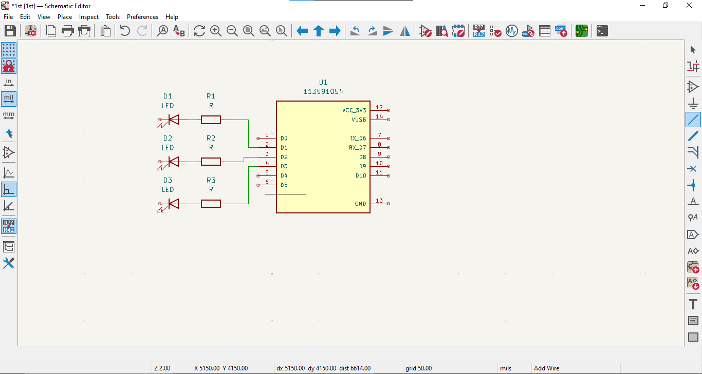
the schematic of 3 LEDs
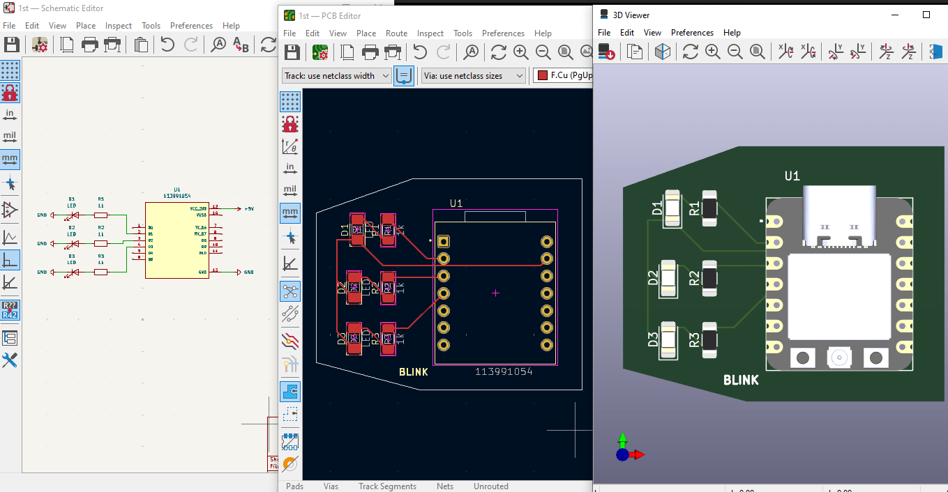
the schematic, PCB tracing and 3D view
For the second part, I shifted focus to the XIAO-RP2040. I downloaded the FabCloud KiCad library from FabCloud GitLab and followed the setup instructions.
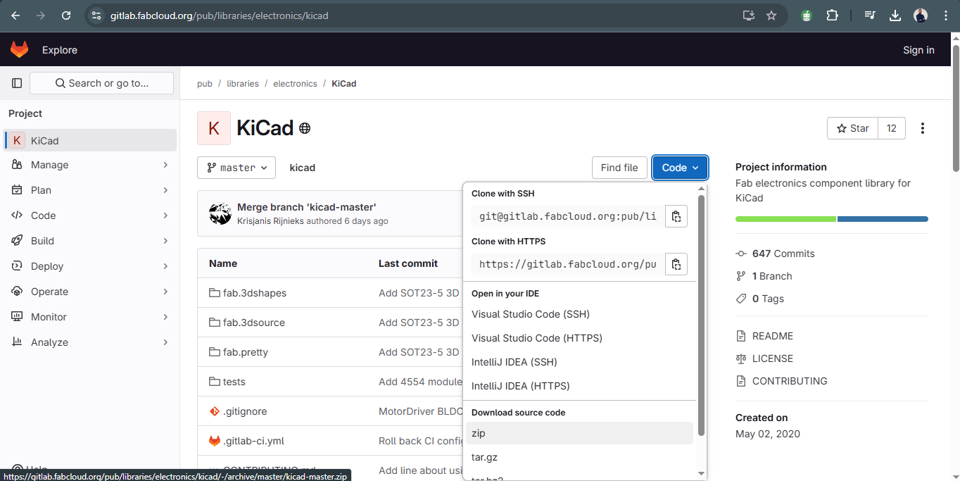
Downloading the FabCloud KiCad library from FabCloud GitLab
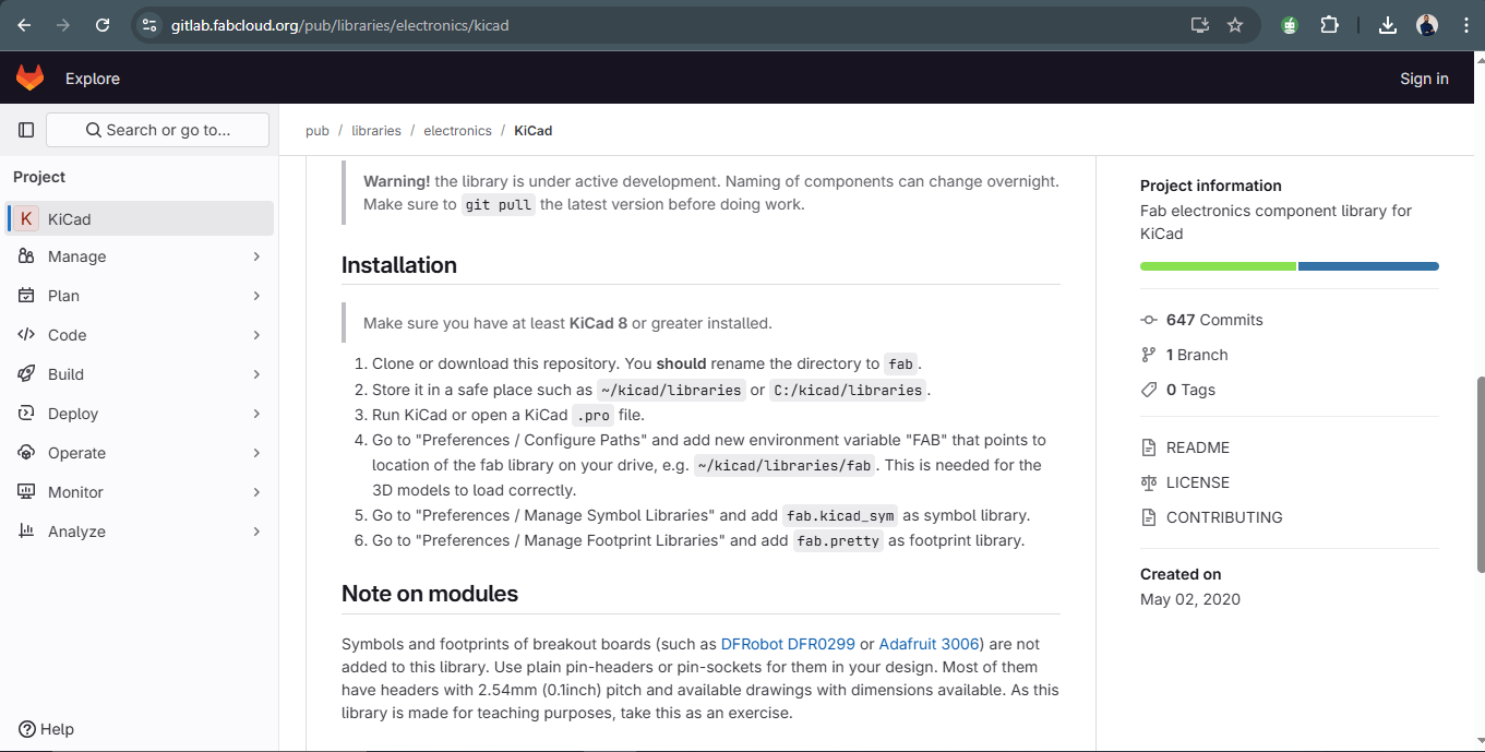
steps to Install it in kicad
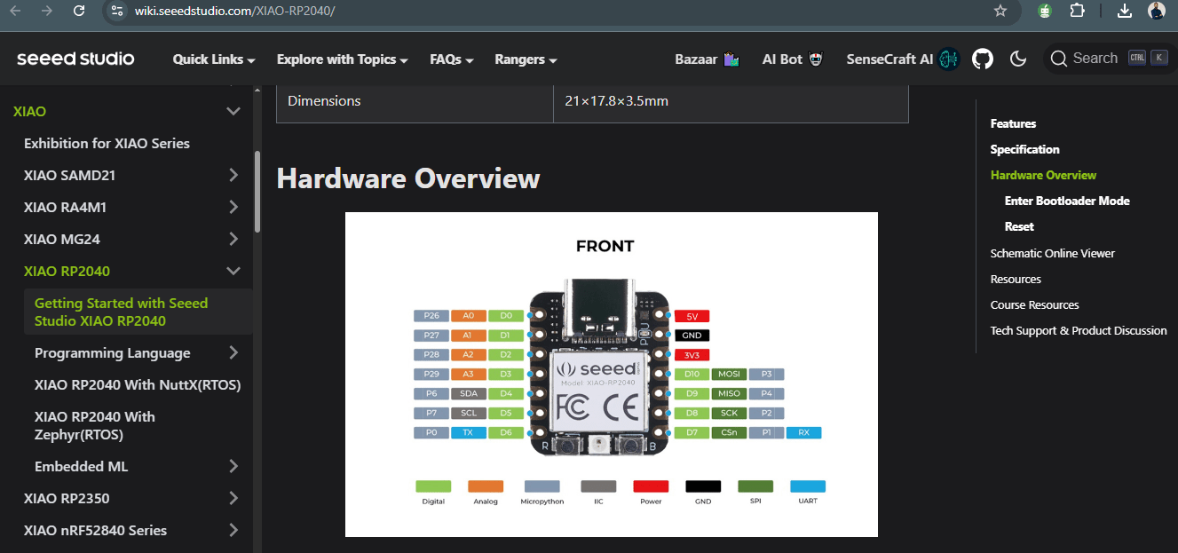
To design the schematic, I first studied the XIAO-RP2040 pinout from Seeed Studio's wiki. I then grouped and labeled pins according to their functions—Analog, UART, I2C, and SPI—and added power and ground lines, a push-button, and an LED.
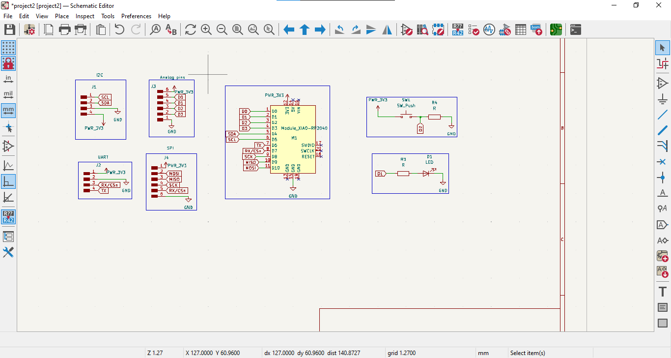
the schematic of my development board
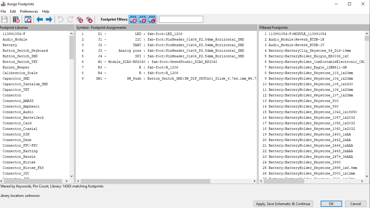
Assigning footprints to the symbols
While the schematic wasn’t too complex, the real challenge came in the PCB layout, where I sometimes had to go back and rearrange connections in the schematic to optimize the trace routing. Eventually, after several iterations, I successfully completed and saved the board.
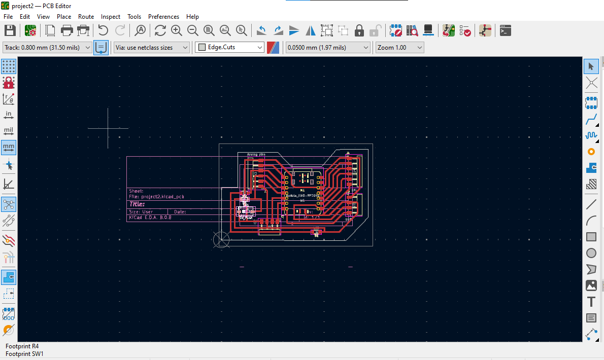
PCB layout and trace routing
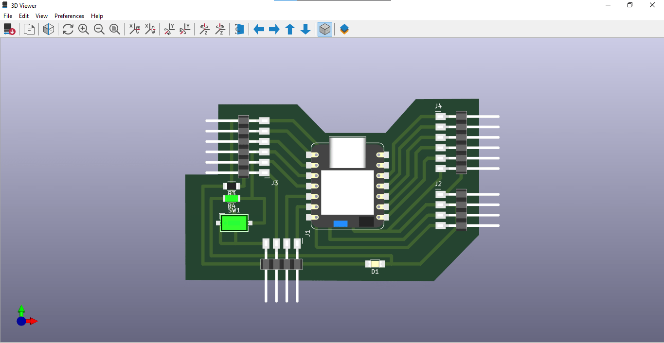
3D view of my development board
Reflection and Takeaways
This project was a major learning curve and gave me a strong foundation in using KiCad, especially in importing libraries, understanding footprints, and refining PCB layouts.
My advice to anyone new to electronics design: take your time learning the tools, don’t fear mistakes, and explore community resources like SnapEDA and FabCloud—they make the work much easier.
This project helped me understand the full cycle of designing with microcontrollers—from circuit planning to PCB design—which will be incredibly valuable in my future hardware projects and prototyping goals.
Design files
- download file (kicad_schematic)
- download file (kicad_pcb)