6. Electronics Design
Group assigment
- Use the test equipment in your lab to observe the operation of a microcontroller circuit board (as a minimum, you should demonstrate the use of a multimeter and oscilloscope)
- Document your work on the group work page and reflect what you learned on your individual page
Link to Group page: Electronics Design
Individual assigment
- Use an EDA tool to design a development board that uses parts from the inventory to interact and communicate with an embedded microcontroller
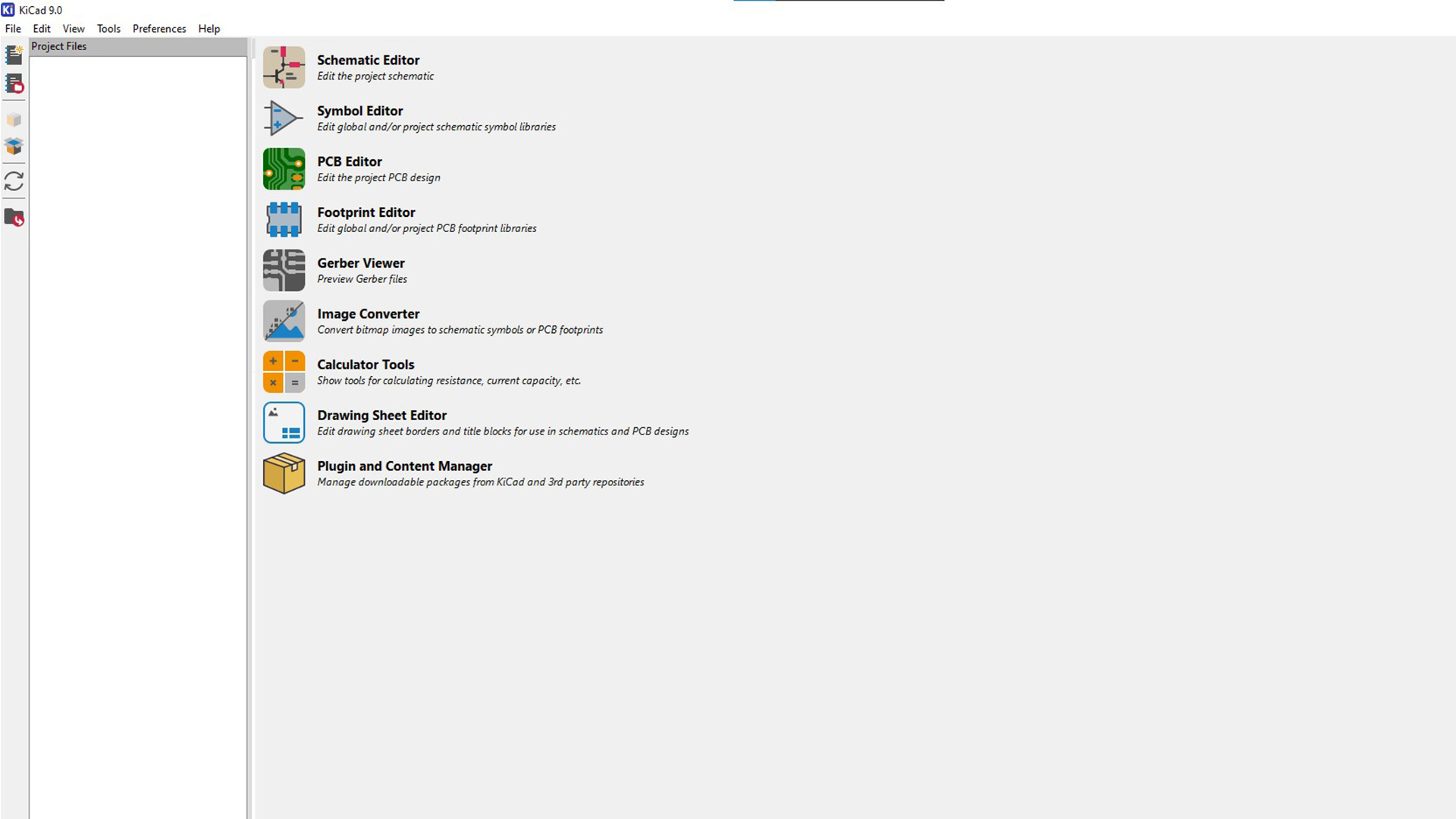
KiCad is an open-source, free electronic design automation (EDA) suite. It helps engineers, designers, and hobbyists to design schematic diagrams (electrical circuit drawings) and printed circuit board (PCB) layouts (physical layout of the circuit board)
Additionally, it also supports the design of component libraries (symbols and footprints), 3D visualisation of the PCB and generation of manufacture files such as Gerber files.
Choosing the Microcontroller
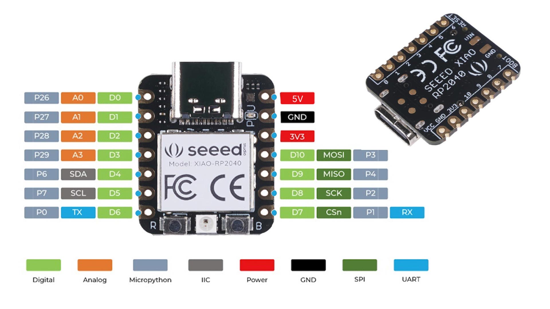
First step, I selected the microcontroller Xiao rp2040
The XIAO RP2040 is a small but powerful microcontroller board manufactured by Seeed Studio, based on the Raspberry Pi RP2040 chip. It contains a dual-core ARM Cortex-M0+ processor clocked at up to 133MHz, 264KB of SRAM, and 2MB of built-in flash. Even though it is small in size (20x17.5mm), it offers 11 programmable multifunctional I/O pins and a USB-C interface, and is ideal for small applications like wearables, IoT, and robots. It can be programmed using Arduino IDE, MicroPython, and CircuitPython.
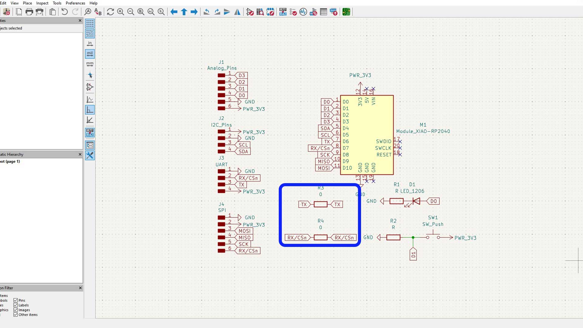
Designing the Schematic with KiCad
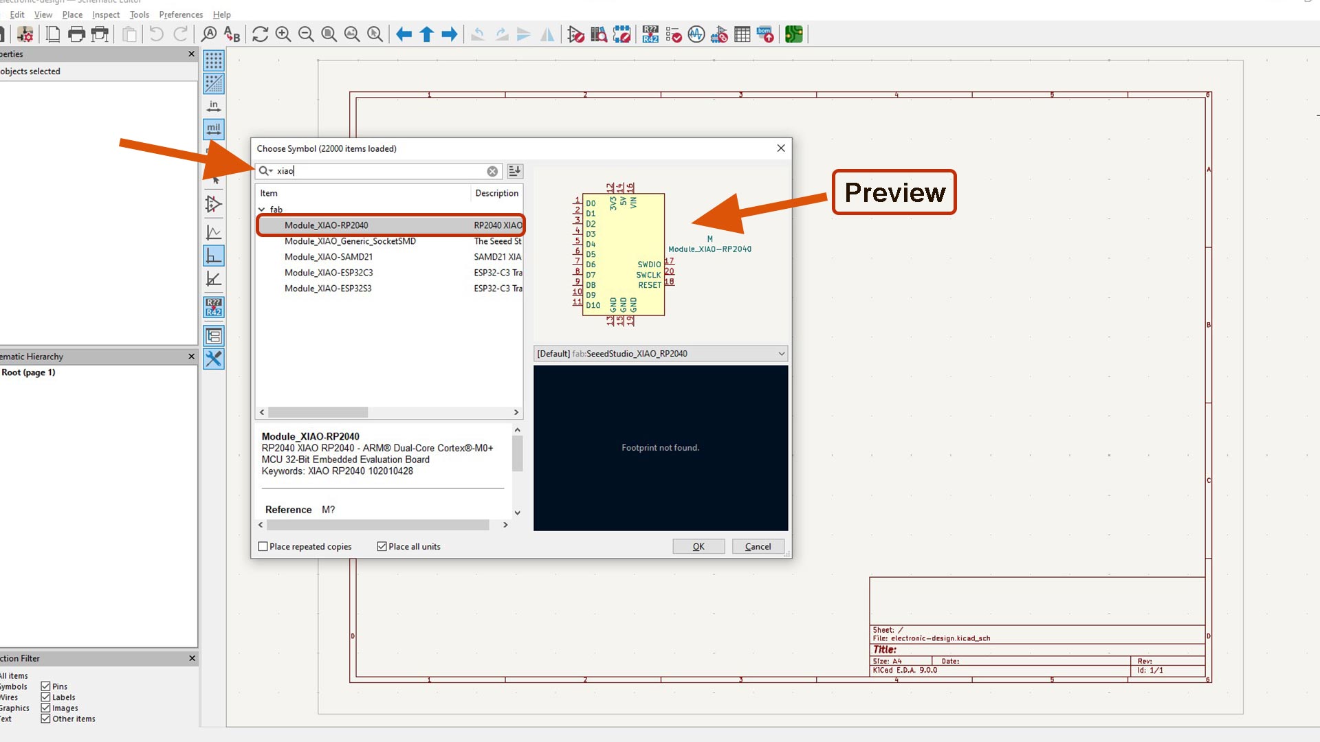
After Placed the XIAO RP2040 symbol:
- Added extension pins to easily access all microcontroller pins
- Added essential components such as power lines (VCC and GND), LEDs for status indication, and resistors where needed.
I grouped related pins together for easier routing.
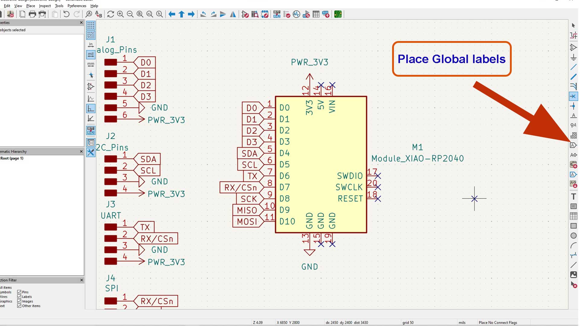
Connecting Components
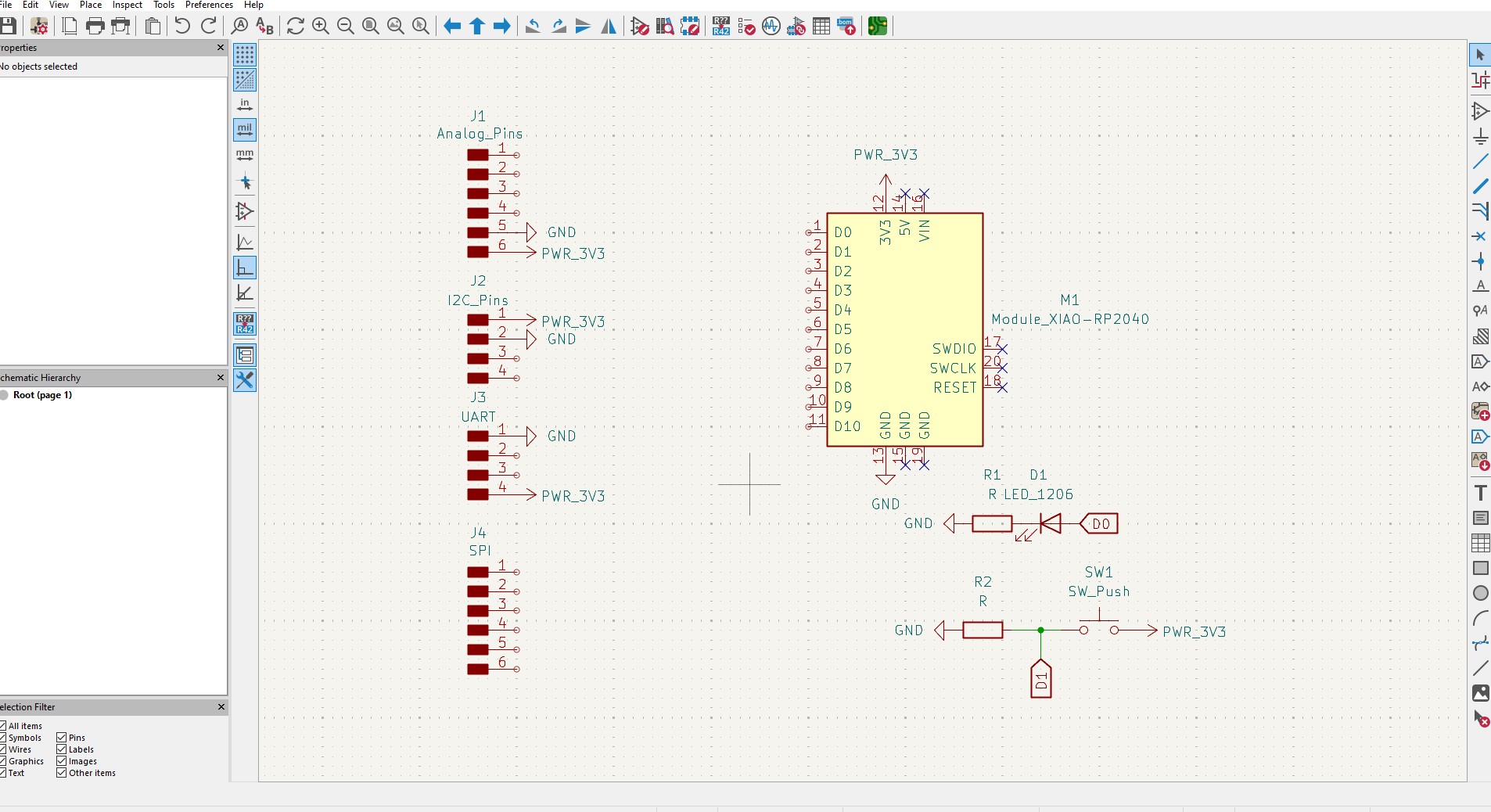
Using Global Labels, I connected each component to their respective correct microcontroller pin
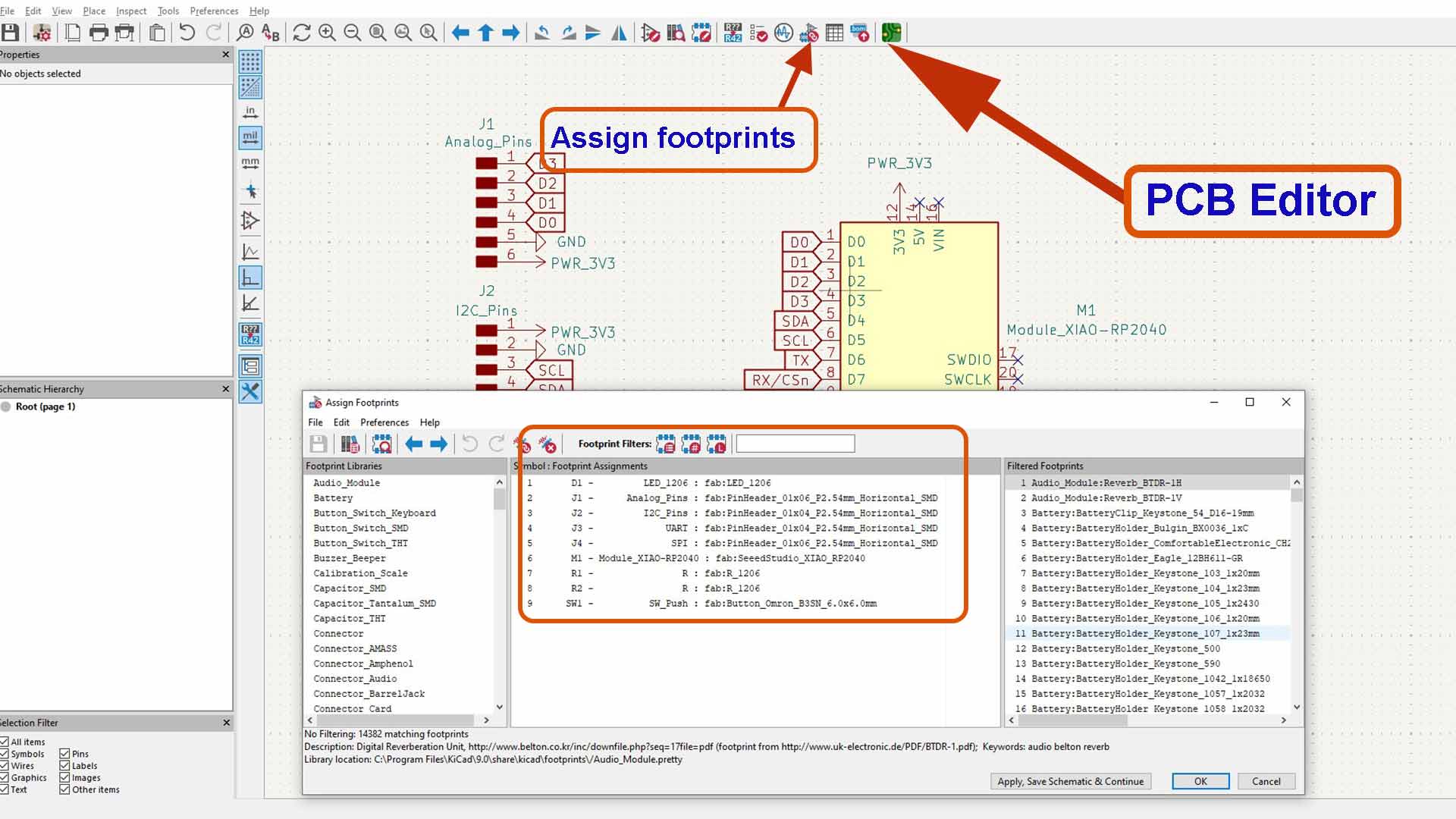
Assigning Footprints
After completing the schematic, I assigned proper with footprints to each component:
- XIAO RP2040 footprint
- Standard 2.54mm headers for extension pins
- LED and resistor footprints
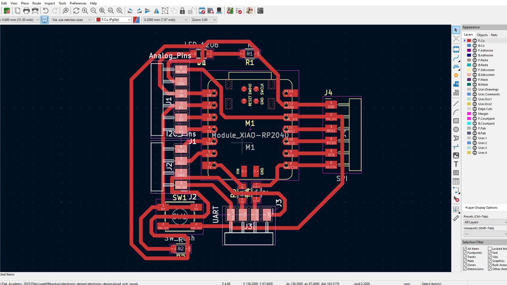
I opened PCB Editor to trace pcb tracks
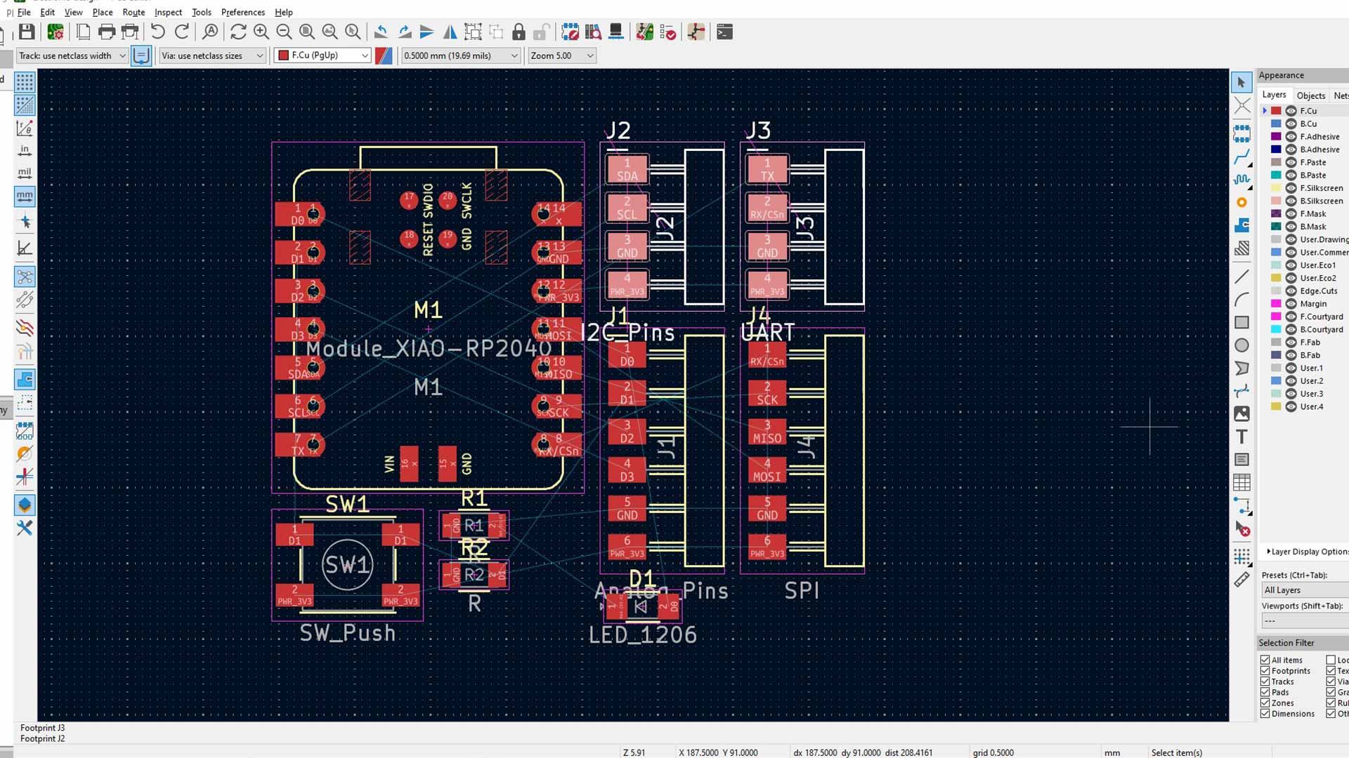
PCB Layout
After, I switched to the PCB Editor to:
- Arrange components with good spacing and logical flow.
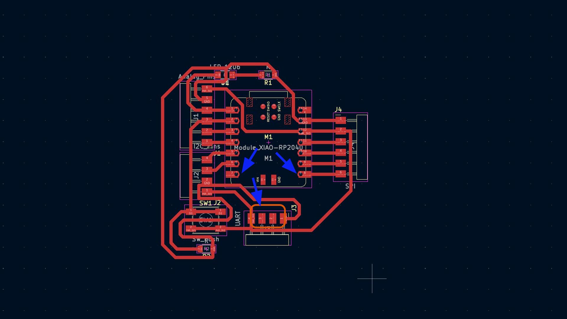
- Route tracks manually, ensuring clear signal paths.
- Add ground planes to minimize noise.
Handling Crossings
When connecting almodt all components, I found that some traces had to cross each other. Therefore, I added 0-ohm resistors as jumpers to maintain single-layer PCB design without violating electrical isolation.
Updated pcb
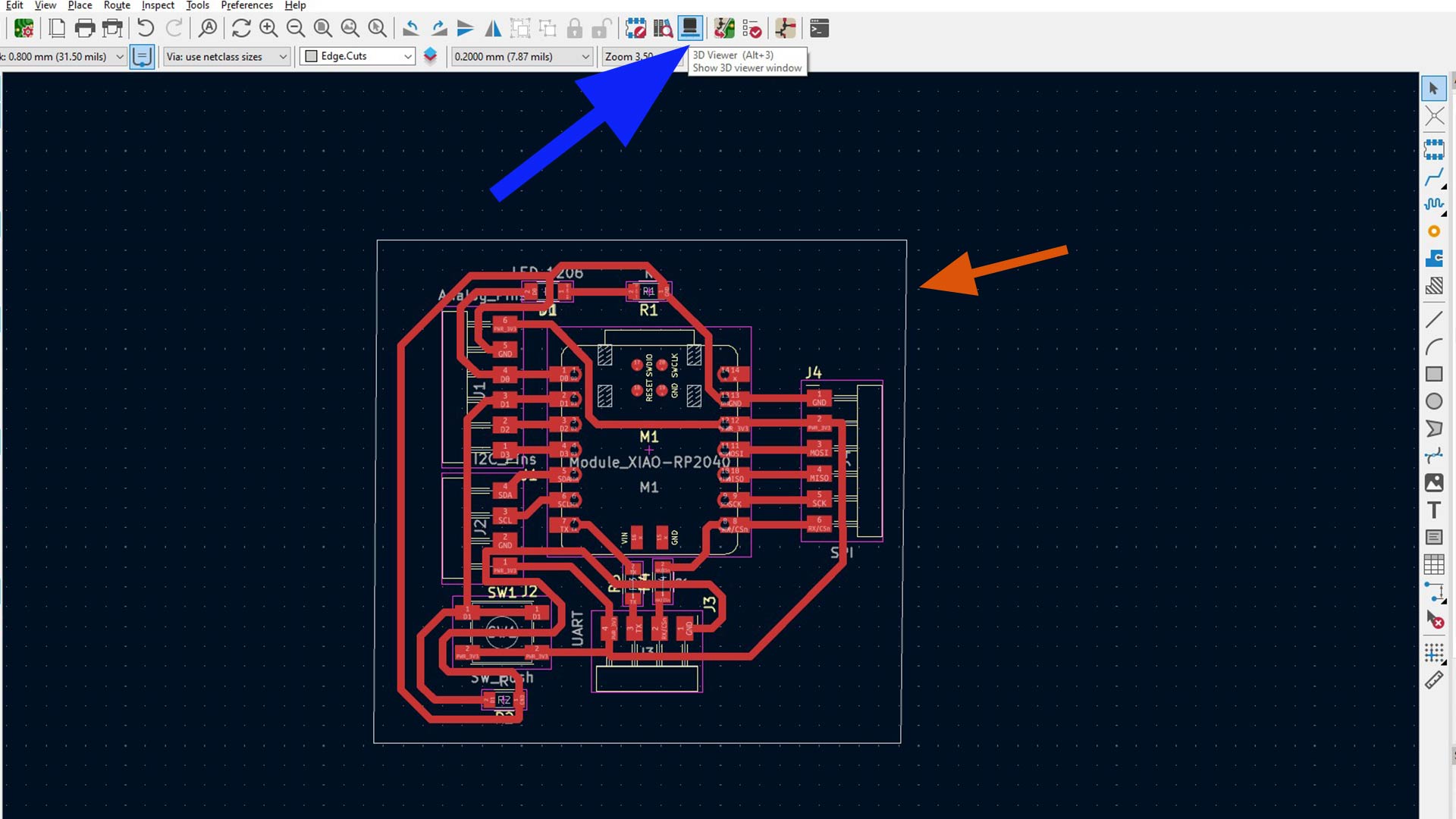
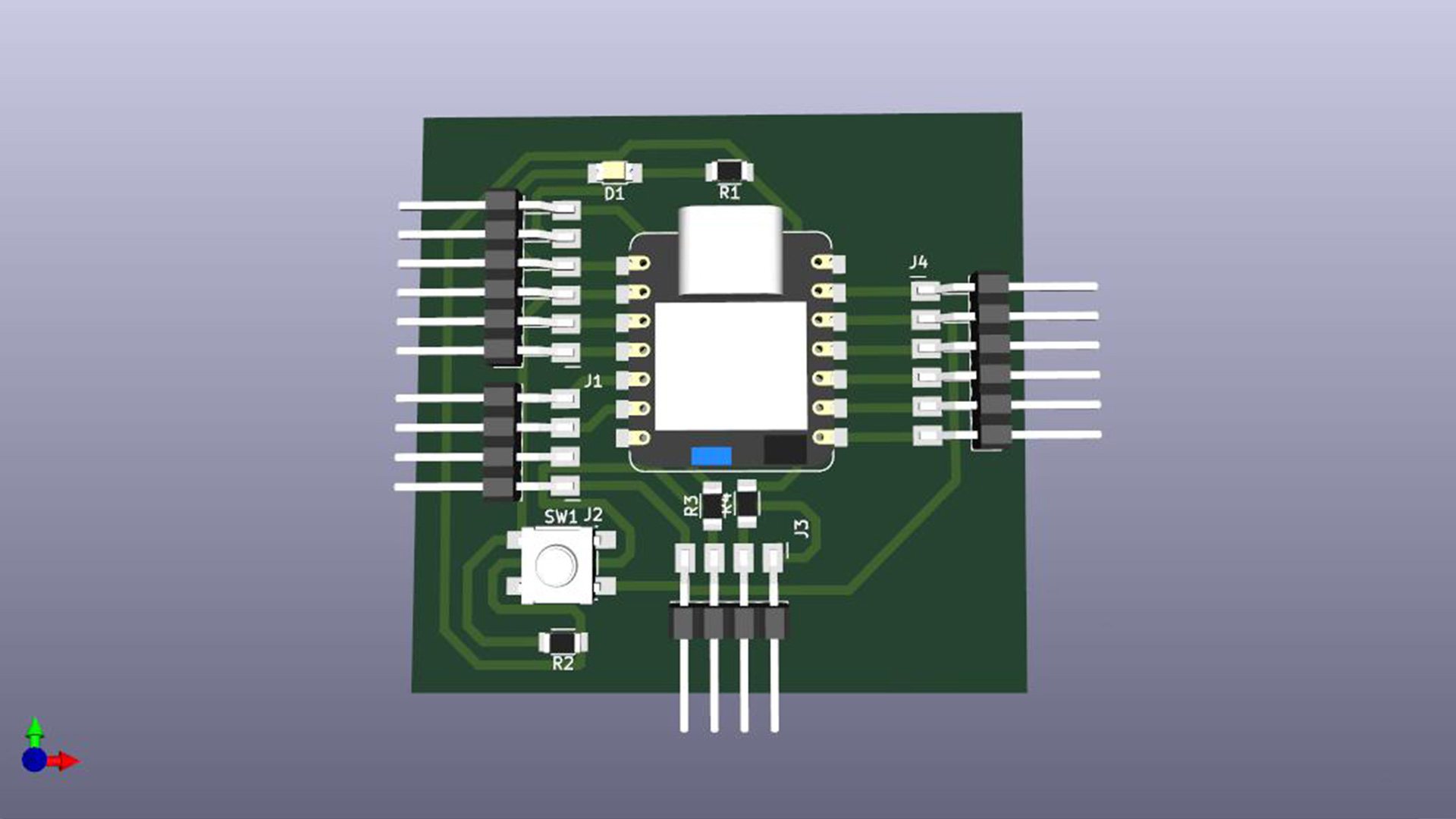
I then opened pcb 3D Viewer to visualize my pcb in 3D
3D Visualization
Finally, I used KiCad’s 3D Viewer to visualize the completed PCB, check component placement, and ensure everything fit properly.
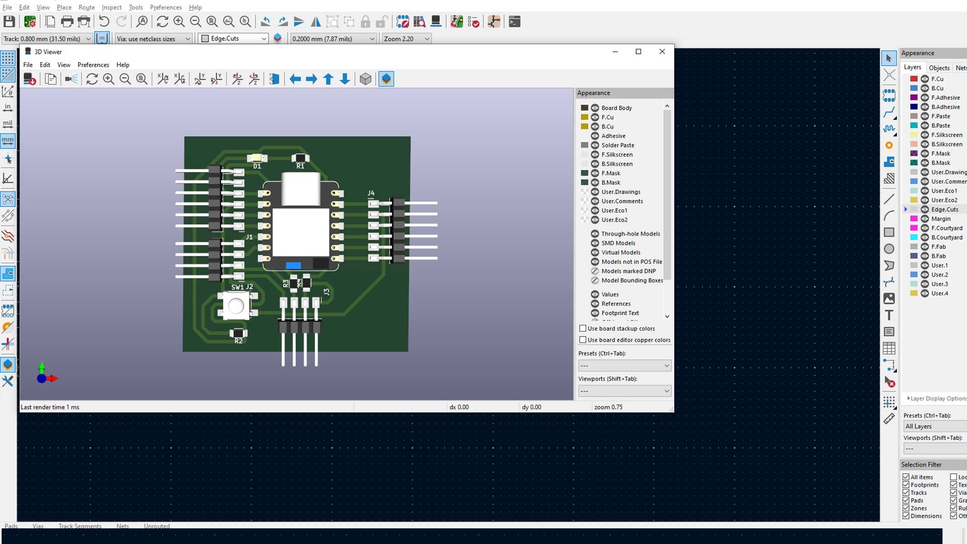
Final Result
- Clean, compact PCB ready for fabrication.
During this week, I learned more about practical PCB design strategies like grouping signals, using global labels, and managing trace crossings with 0-ohm jumpers.
Download files
Here you will find the original files I designed
PCD Design