8. electronic production
During week 08 of the Fab Academy, I tackled the horrible integral process that combined theoretical and practical knowledge in the manufacture of electronic circuits (which I really don't know a thing), focusing on the production and testing of an engineered microcontroller development board. (originally developed in week 06 of the FAB), but also to research, test and see about design tools, manufacturing techniques and criteria within the electronics production chain.
Electronics Production
Circuits were previously built by hand using point-to-point wiring, this was really error-prone, difficult to maintain and not very scalable (just like the egg you were given to take care of in elementary school). Over time, the use of perfboards and breadboards emerged, which made prototyping easier, but were still inefficient.
The solution came with the development of Printed Circuit Boards (PCBs), which replaced messy wiring with copper traces engraved directly onto a rigid board, increasing reliability, miniaturization, and mass production.
In this week of the Fab Academy, this process is taken to an educational and practical level, allowing us to design, fabricate and test our own boards using tools from the Fab Lab.
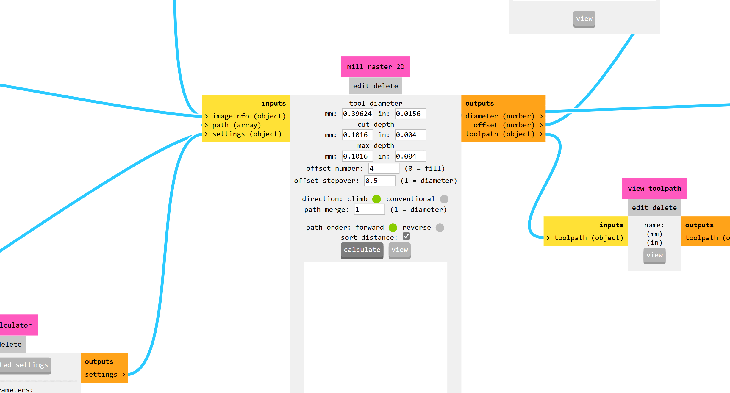
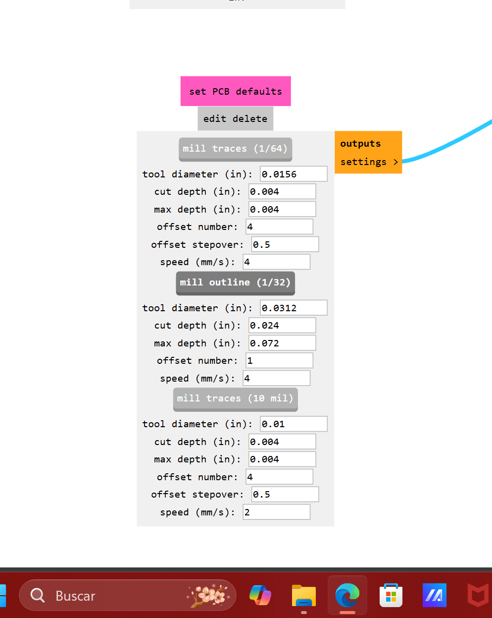
SVG Export and Toolpath Generation
With the SVG files generated in KiCAD (layers F.Cu, Edge.Cuts, and User.1), I used the Mods CE platform to generate the toolpaths (.rml) for milling. These routes include:

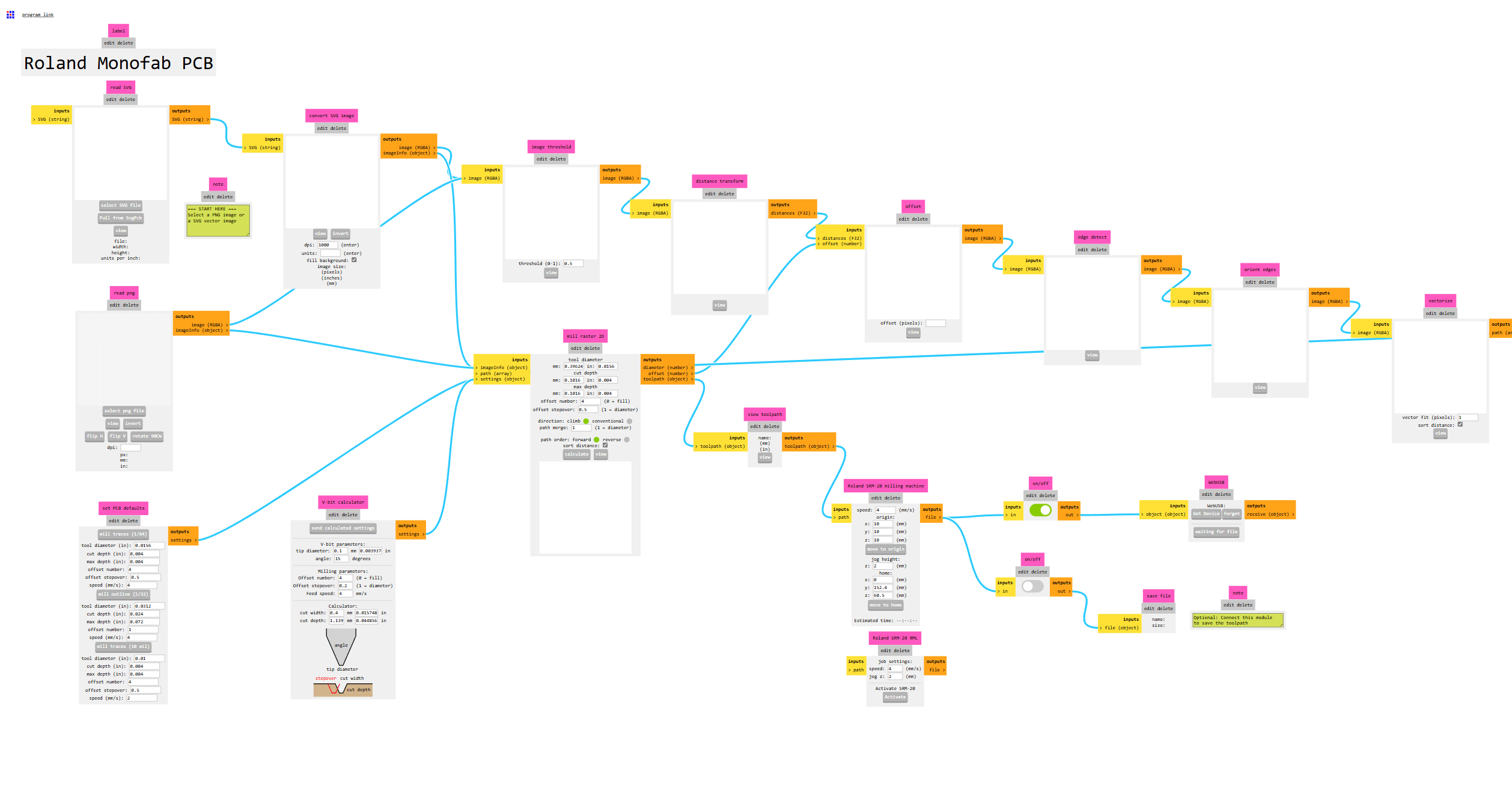
The files were organized in the order of execution to avoid errors during the operation.
Roland SRM-20

The machine used was a Roland monoFab SRM-20, equipped with dust protection and tool projection. I installed the necessary software and performed the following steps:
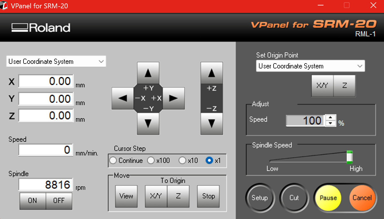
(In this part we will have to be careful with the Z axis since first we will have to turn on the repetitions per minute that are approximately 8000-9000 rpm, and lower the bit with the stepping, until it barely rubs and the change in sound is heard when it gently impacts with the copper).
Milling cut
in this case we are going to use a 1/64 bit for the traces and this tip.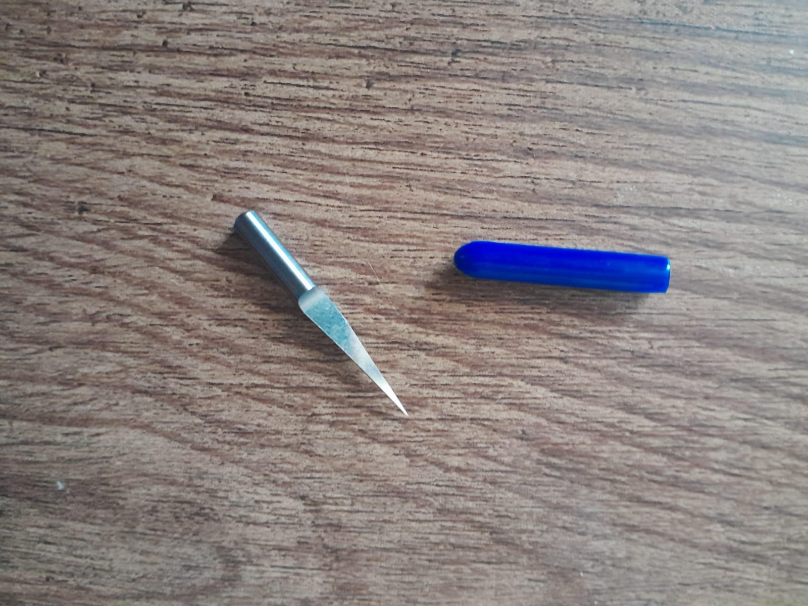
You could use Ferric Chloride in PCB Manufacturing...but it pollutes too much so fabacademy will not accept this method.
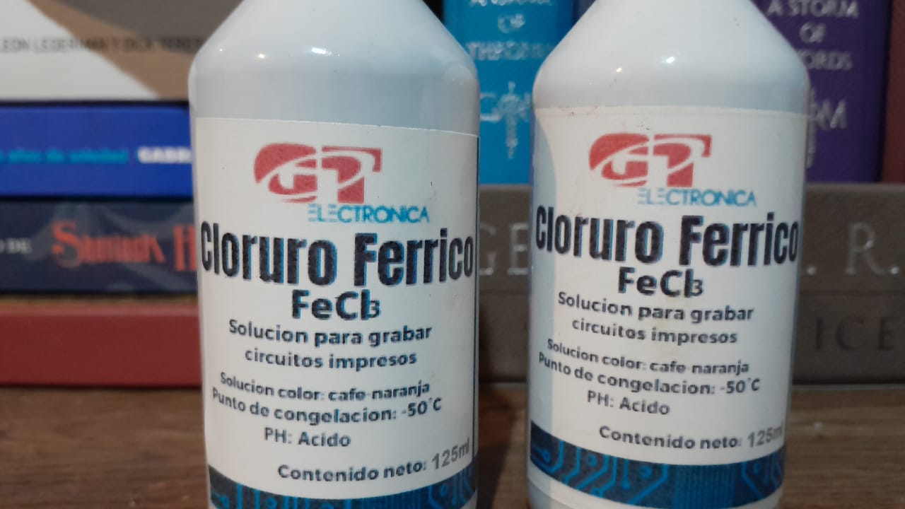
Ferric chloride (FeCl₃) is one of the most commonly used reagents (and theoretically the traditional method and the most contaminant) in the chemical etching process of printed circuit boards (PCBs), especially in prototyping labs and DIY electronics workshops. This dark brown, water-soluble compound acts as a corrosive agent capable of dissolving unwanted copper on a PCB sheet, thereby revealing the circuit design previously transferred to the board.
Design Preparation
The process begins with preparing the circuit design, usually created using electronic design software and then printed onto a transparency or glossy paper using a laser printer. This design is transferred to the copper surface of a blank PCB using heat transfer methods or a UV exposure unit.
Chemical Etching Process
Once the design has been properly transferred, the chemical etching step begins. A ferric chloride solution is prepared, typically in a plastic container, as this compound is highly corrosive and can react with metals. The board is submerged in the solution and agitated constantly. Ferric chloride quickly reacts with the exposed copper areas, dissolving them while leaving the parts covered with toner or photoresist intact.
Etching Time and Cleaning
Etching time may vary depending on the ferric chloride concentration and the temperature of the solution, but generally ranges between 10 and 30 minutes. Once all unwanted copper is removed, the board is rinsed thoroughly with water to stop the chemical reaction and cleaned with acetone or isopropyl alcohol to remove the toner or mask, revealing the copper traces ready for drilling or soldering electronic components.
Safety and Environmental Considerations
It is recommended to use gloves, safety goggles, and work in a well-ventilated area to avoid direct skin contact or inhalation of fumes.
Since the waste solution should not be poured down the drain due to its high environmental toxicity, it must be stored in a sealed container for proper disposal at a hazardous waste facility.