6. Electronics Design
                                 .@@@@@@@@@@@@@@@@@@@@@@@@@@@@@@@@@.
                                @@@@@@@@@@@@@@@@@@@@@@@@@@@@@@@@@@@@@
                              @@@@@                              :@@@@@
                      +@@@@@@@@@@.                                 -@@@@@@@@@@@@@@@
                    -@@@@@#####:           =             :           -##########@@@@@
                  .@@@@@  ++        +.    :..  .:. .:.  -.:    .:     :#######*  .@@@@@
                 @@@@@. .+-: .   .  :  .. :.   =@:#-@:# :..  .  +  ..@%.......:@#  :@@@@
               @@@@@. :@@@%%@@@@@@@@@@@+:     . : @ : @     .%@@@@@@@. *##%##:  =@+ -@@@
             @@@@@: .@% .+#%+-   :.:+-:-: .:  .:#.#.#.% ..: .::-#:.. %@-..  .%%   @.-@@@
           %@@@@=  %@.:%%@@@@%%%@%@@@@@=: :   .:*.%.*.# : . .#@@@@@%@=.+%%::.@@:. @.-@@@
         *@@@@*  #@:.%%.:=#%=-   .=*##*-: .          .  . . .-*#@*=.  .#@@ : @@%. @.-@@@
        @@@@%  *@- #@: -+%@@@*==+=%@@@@-:                   .=@@@@#.   .@#*=%..@. @.-@@@
        @@@@ .@+ *@- -@*=*@@#=::::%@@@@-:        :*+        .-@@@@#.  ..+%@@%  @  @.-@@@
        @@@@..@ .@- %%..:+@@#-  ..#%@%@-:        -++        .:@%@%#:.:*%+-:%@.:@  @.-@@@
        @@@@.@@% @-#@@-:.*@@@*++++@@@@@=:         .         .+@@@@@+=+%@+. %@::@  @.-@@@
        @@@@#::::@#-::- :=#%=-   .=+#**::                   ..**%+=.          .@  @.-@@@
        @@@@-#%# @+*%%-:.*@@@%%%@%@@@@@+:                   .#@@@@%.    +@%.   @  @.-@@@
        @@@@ *@= @--@%..:=-+.-   :.:-::-:                   .::-*..:  :--+==- =@  @.-@@@
        @@@@ .@.=@# @+  .#%@@@@@@@@@@@@+:                   %@@@@@@@%@@@%*:@@@%   @.-@@@
        @@@@ .@=*%#.@+  .=-=.-   :..-:.-:            .    +@+-::* .: ...#@@%@..   @.-@@@
        @@@@ :@*::.-%+  .#%%@@@@@@@@@@@+:     ..: :.:..   @+.%@@@@@%%%@@+: @@:.   @.-@@@
        @@@@ .@.%@@.@+  .=%@=-    -=+=-.:    .@*@=.#@#@   @*. =@@=:.  -+=-:++.. .%% =@@@
        @@@@ .@: @: %+              =          +@-.*@*=   @+   @#     .--------%@..@@@@@
        @@@@ .@. @= *@:                ........:::.:::::::@*...@+    %%-:::::::. @@@@@:
        @@@@@ =@+ #@- %@-:::::::::::::::::.          :-@@@#   #@@    @.     @@@@@@@@=
         +@@@@# +@= #@: ------------------#@:        :-@@=:   #@@    @.   @@@@@@@@*
           #@@@@+ #@- %@@@@@@@@@@@@@@#:::.:#%:      ...--.::. :-- *  @. #@@@@+
             @@@@@- #@**********-    %@%.:=@@-:    ::     -=:     *  @. @@@%
               @@@@@:           #@+=+@@%.-+@@=:   .%#     =@:     *  @. @@@-
                 @@@@@@@@@@@@@@      ===**+=%@%##.:*+     @%-     *  @. @@@-
                   @@@@@@@@@@@@@#       #*-     .@% . .....: .....*  @. @@@-
                             #@@@@=..........     :@**=@@+*.:=#@@:=.%@  @@@-
                               @@@@@@@@@@@@@@@-     -##@@##***%@@***:  @@@@-
                                 *#########@@@@@.....:....-..........%@@@@=
                                             @@@@@@@@@@@@@@@@@@@@@@@@@@@*
                                               .::::::::::::::::::::::
This is sixth week of the Fab Academy!
(one of the ones I really hate the most so far).
groupal assignments
group assignmentsAt Fablab Puebla, we are equipped with a laboratory that includes 22 Gwinstek oscilloscopes and 20 Hioki multimeters—essential tools for analyzing electronic circuits. Both devices allow for the measurement of electrical characteristics, but they differ in their main purpose: the multimeter provides numerical readings of voltage, current, and resistance, while the oscilloscope offers a visual representation of how electrical signals change over time. During our practice sessions, we began by exploring the basic functions of the multimeter. We tested for continuity, which is crucial to ensure correct connections between components on our PCBs. We also measured the resistance of specific components, such as R5, confirming that it matched the theoretical value. Additionally, we tested diodes and LEDs using the diode test function, which also revealed the LED’s color by lighting it up. Next, we performed voltage measurements on powered boards. In one measurement, we observed a value of 5.172V. Although this initially seemed high, our instructor explained that it was within the USB’s acceptable tolerance range (+/- 5%). Using the oscilloscope allowed us to analyze signal behavior in real-time. We tested a no-delay blinking code on an RP2040 microcontroller and observed a square wave with a frequency of 912.3 kHz. From this signal, we learned how to interpret parameters such as rise and fall times, amplitude, peak-to-peak voltage, and phenomena like overshoot, which occur due to impedance mismatches in real-world circuits. We also explored the use of the oscilloscope’s cursors to accurately measure time intervals and voltage levels. In later tests, we generated a PWM signal with a 20% duty cycle, confirming its frequency (~500 Hz) and duty cycle (~19.96%) using the oscilloscope’s automatic measurement features. Another interesting activity involved visualizing a UART signal transmitting the character "Z" at 9600 baud. We clearly identified the start and data bits and measured the time intervals between transmissions, confirming the protocol’s accuracy. Finally, we analyzed a sine wave generated by an ESP32 DAC board, measuring its RMS voltage, amplitude, and average cycle level.
individual tasks
In PCB design this week I opted to show my own design, as I feel it's repetitive (although it's almost the same).
Building circuits that enable electrical signals to carry out particular tasks is known as electronic design. Circuit layout on a PCB, schematic design, and component selection are all steps in this process. A printed circuit board, or PCB, is a tangible platform that uses conductive traces engraved into a non-conductive substrate to link electrical components.
Designing a PCB (printed circuit board) is one of the most significant moments in the process of transitioning from electronic theory to its tangible application.
Development
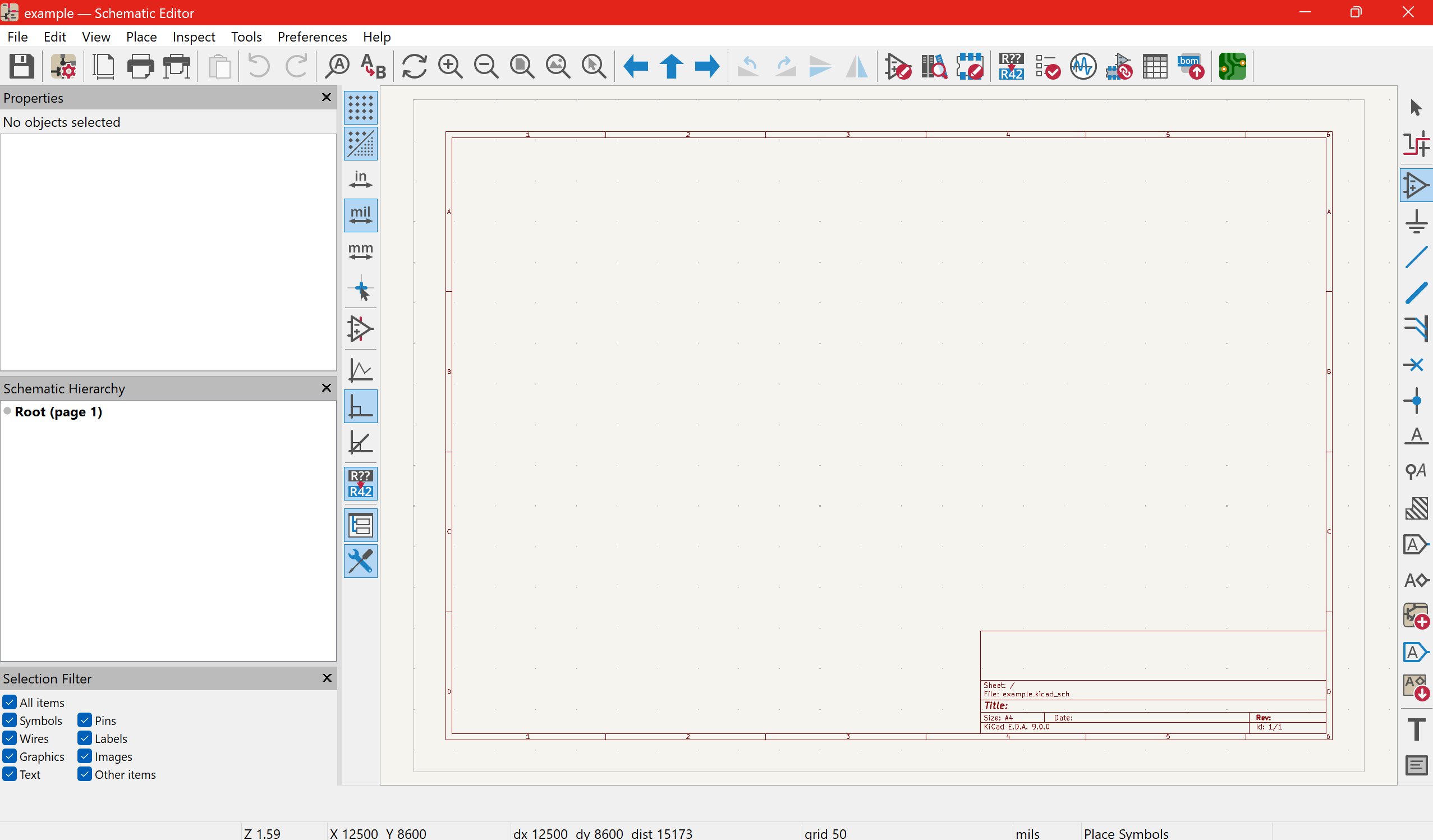
I will start by creating a new project in KiCAD. This action should have generated the essential files for us to work, particularly we will use the schematic (.kicad_sch) and the design of the PCB (.kicad_pcb).
I opened up the schematic editor to begin building the logic circuit that would define the internal connections of my board. (which can be separated between modules and you can organize them as a mind map that reflects your organization in life or not...).

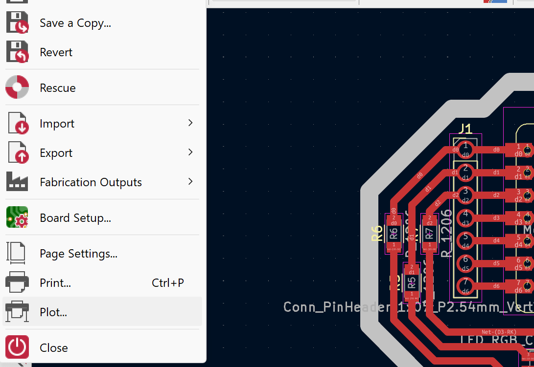
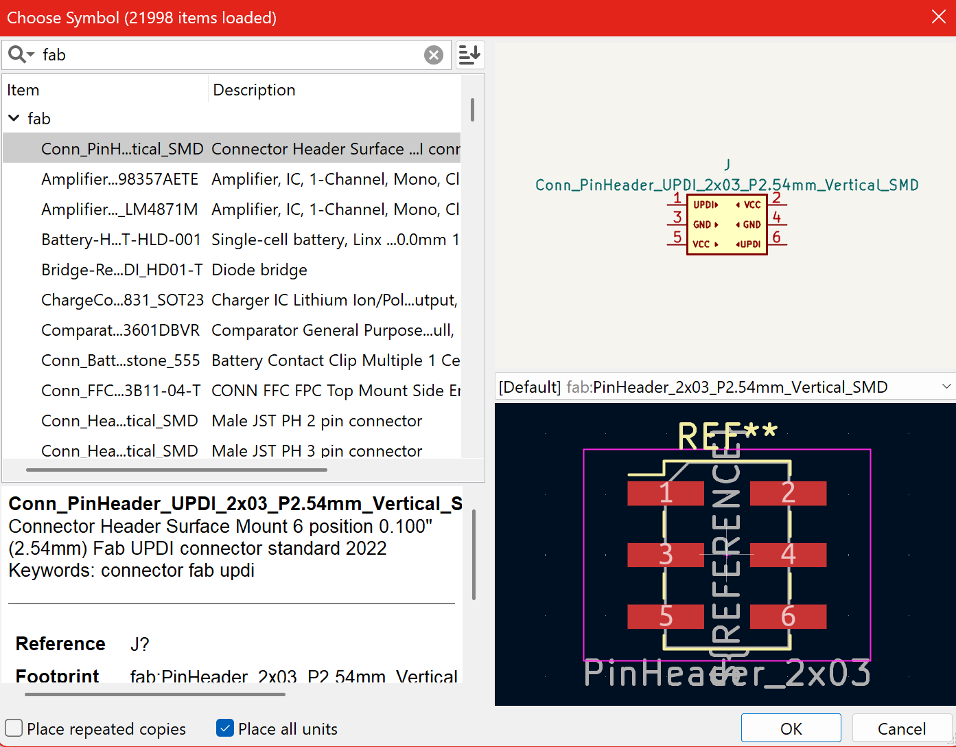
I inserted all the necessary components from the library (using that triangle with a – and a + on it, that is the menu of the available options) including a microcontroller (xiao rp2040), resistors, connectors, and the occasional test LED. The important thing at this stage is to define each part of the circuit before moving on to the physical design.
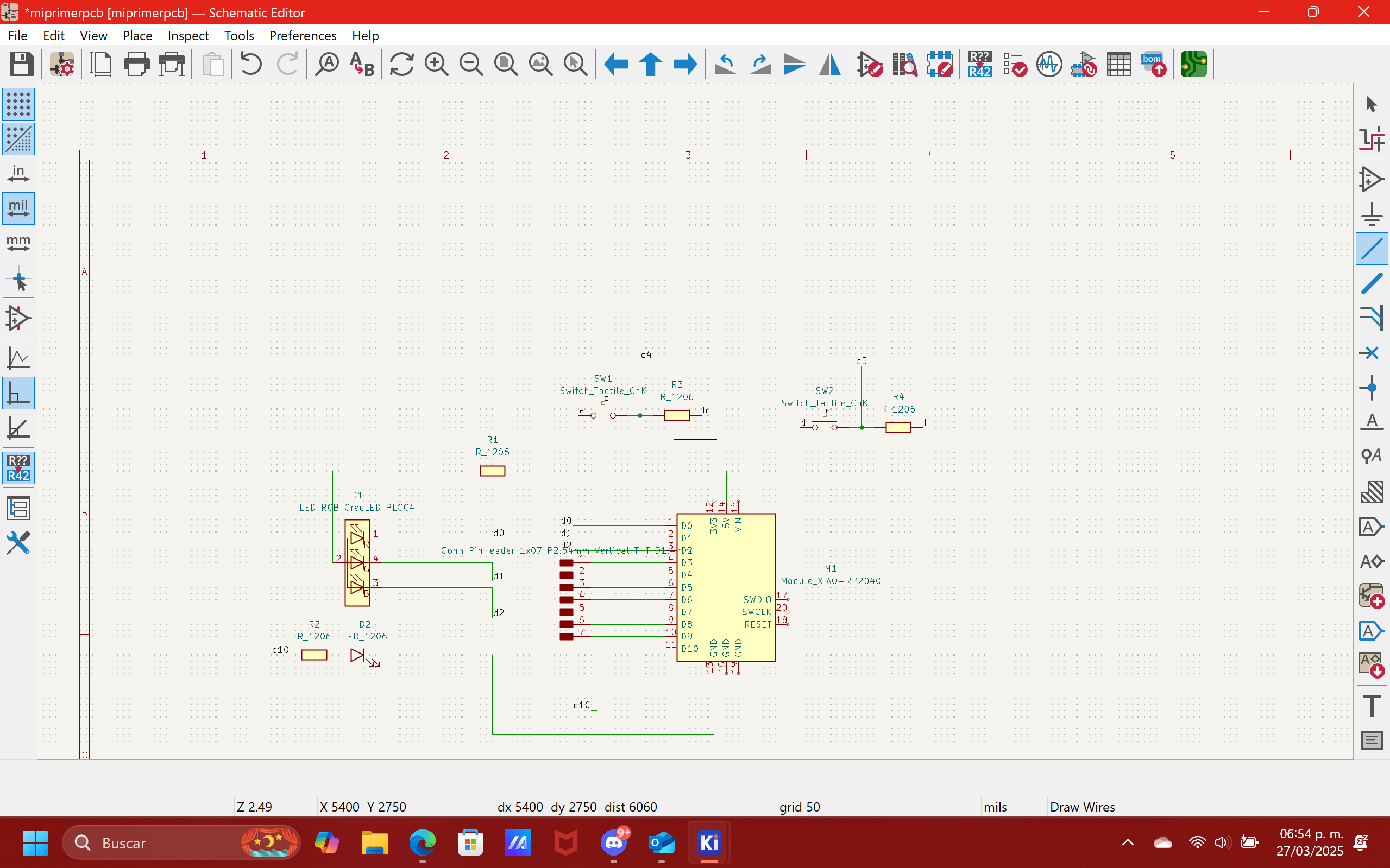
After placing the components, I started connecting them wirelessly (assigning them an outbound input) using wires (W) and labels (L) that helped me to better organize the circuit and maintain a clear nomenclature. I named the important signs as D1,D2,D3, etc, among others, which made it easier to understand the design. Once this work has been done, we will have to verify the fingerprint and that each component was assigned its corresponding value (for example, a 120Ω resistor to limit the current of the LED), as well as a unique reference to easily identify them.
In this design I used a common anode RGB LED, they did not have exactly this fingerprint in the FAB so I had to change the same footprint but for common cathode to a common anode.

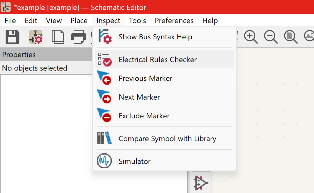
Then it's time to review the design with the ERC (Electrical Rules Check) tool, which detects logical errors or missing connections.
Once the scheme was corrected, I moved on to the most tedious and at some point interesting part in my opinion: the physical design of the board.
Since we have already installed the components of the fab we have the footprints and components assigned correctly so we do not have to worry at least that one occupies a component outside the database of the local fablab in components. (Note: Always check the fingerprint of your components before cutting your board.) Then, upon opening the PCB file and updating from the schematic, the components appeared scattered.
So we will have to start to do the boring task, the task of organizing and rotating each part efficiently to achieve a logical, compact and aesthetic distribution.
With the design already complete, I ran the DRC (Design Rules Check) tool, which allowed me to validate that all the connections were correct and there were no manufacturing errors.
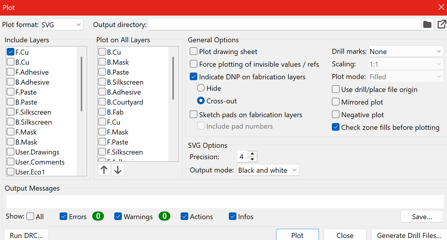
(Note: in this specific part, we may be shown some errors that are not really errors, so we will have to analyze each error shown in the dialog box). Once everything was verified, I proceeded to generate the svg files, essential for the manufacturing process.
In addition! We can see a 3D view of our approximate board.
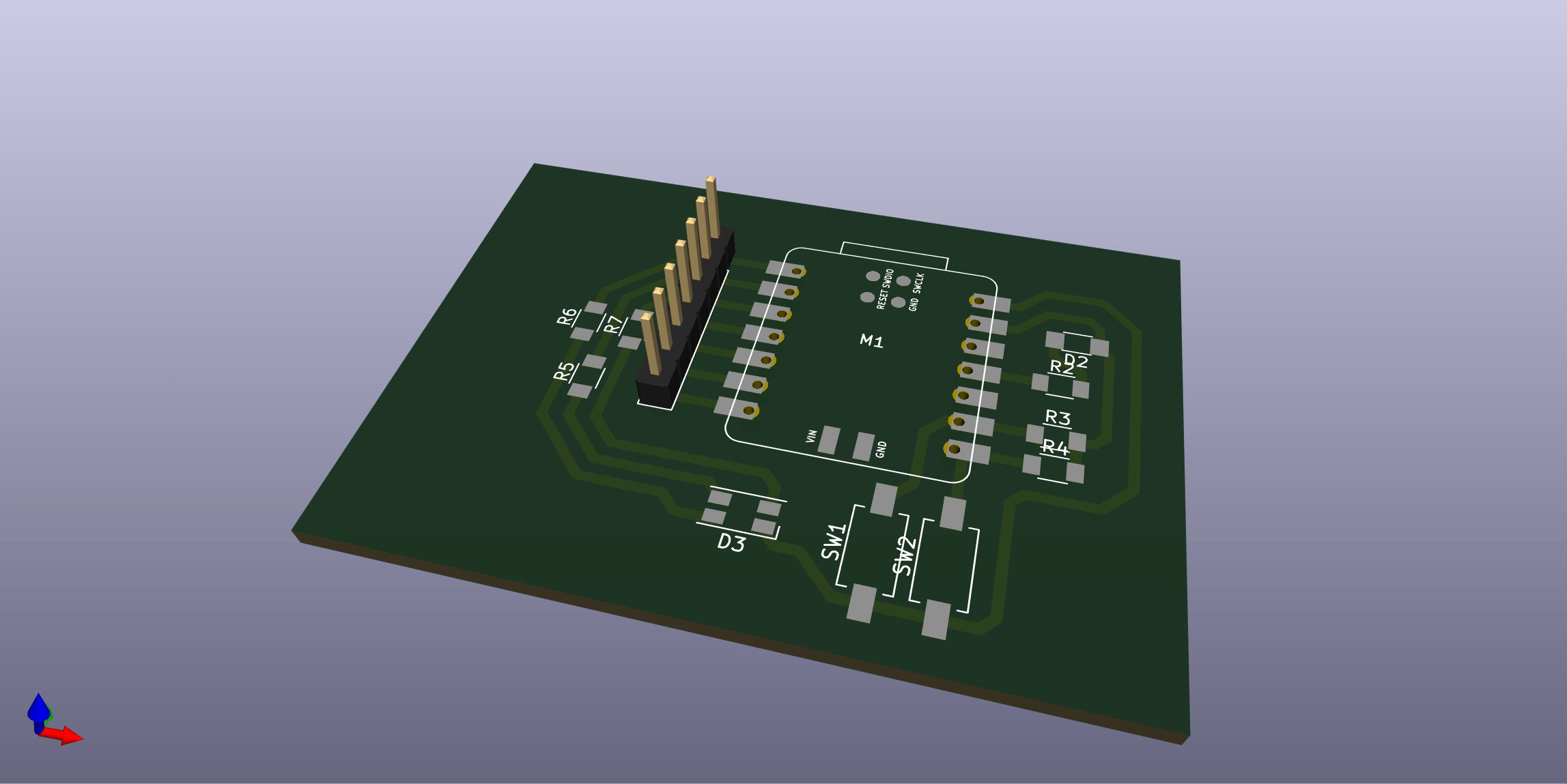
I selected the necessary layers separately (F.Cu, F.SilkS, and Edge.Cuts,). To make sure the design was well represented.