Week 6. Electronics design
hi, still here but just the matter, my mind has already gone too far and I'm barely ending this week but yeah. Electronic design is the topic, this means literally designing those green card with a lot of micro things that turn on and make things. There is a hole process to make one of those and there is a program that helps you designing them. This program is: kicad

But first
Take a look to the Link to the group task
Starting with kicad
First contact
Once you open kicad it will appear a window with many options
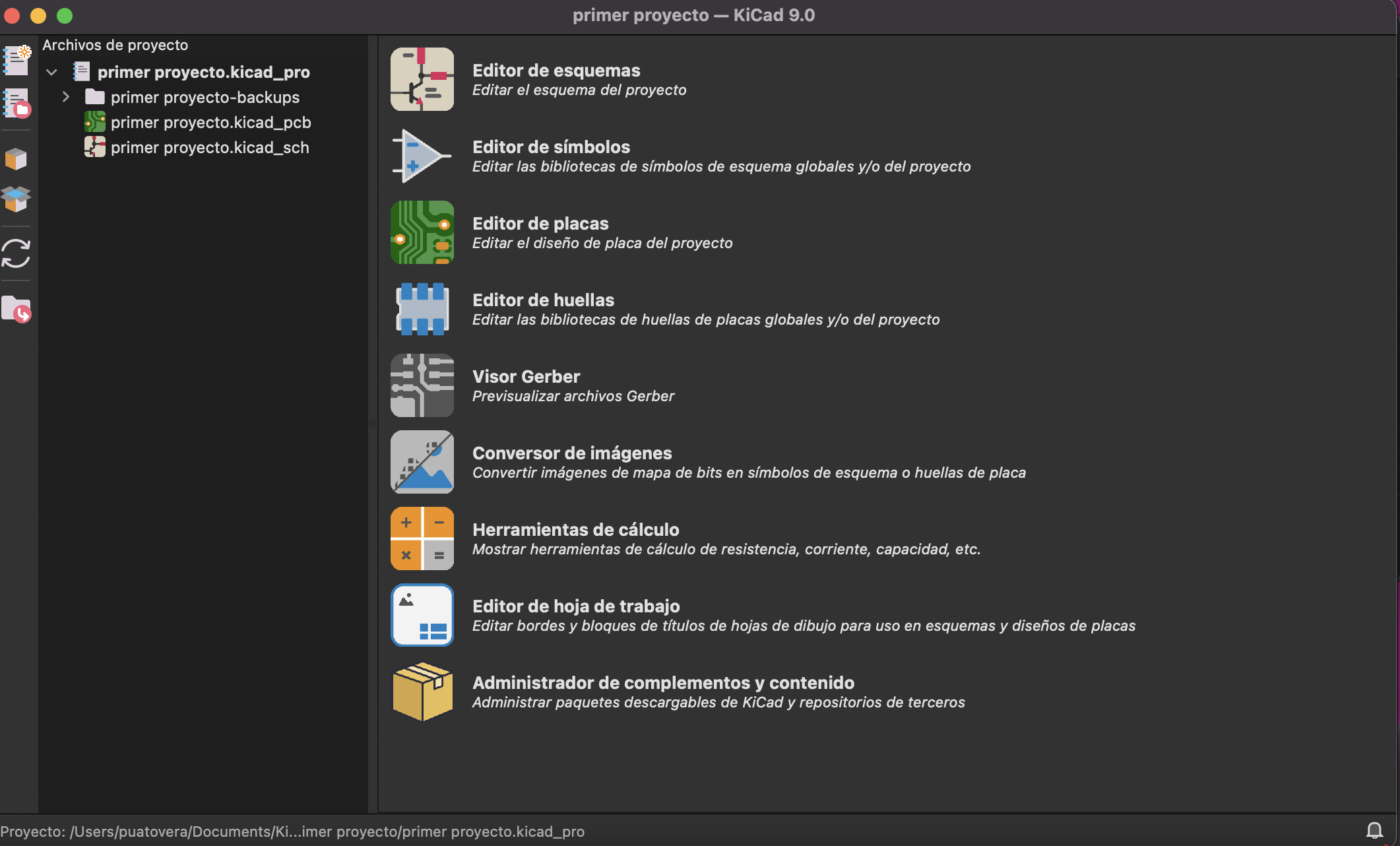
Don't go to fast, there is a little thing we have to do before starting, we have to add the fab library to our program. I guess you already figured out that this has to have libraries to work with.
Adding the libraries
There are 3 libraries we have to add, symbols library, footprint library and manage design block library.
-
Symbols:
the symbols to represent the components and it shapes. -
Footprint:
Like a realistic 2D design of the components so we can design the circuit as close as the real components -
manage design block
A 3D model of the component so we can visualize it before creating it.
I downloaded a library that fab gave us so we can work with the actual material we have here ir our fablab, Important to put that file in a place where you can remember were is it and never move it. In my case i putted it in the same folder as the program.
Adding the libraries
To access this libraries we have to go to the very top menu on the "preferences" submenu.
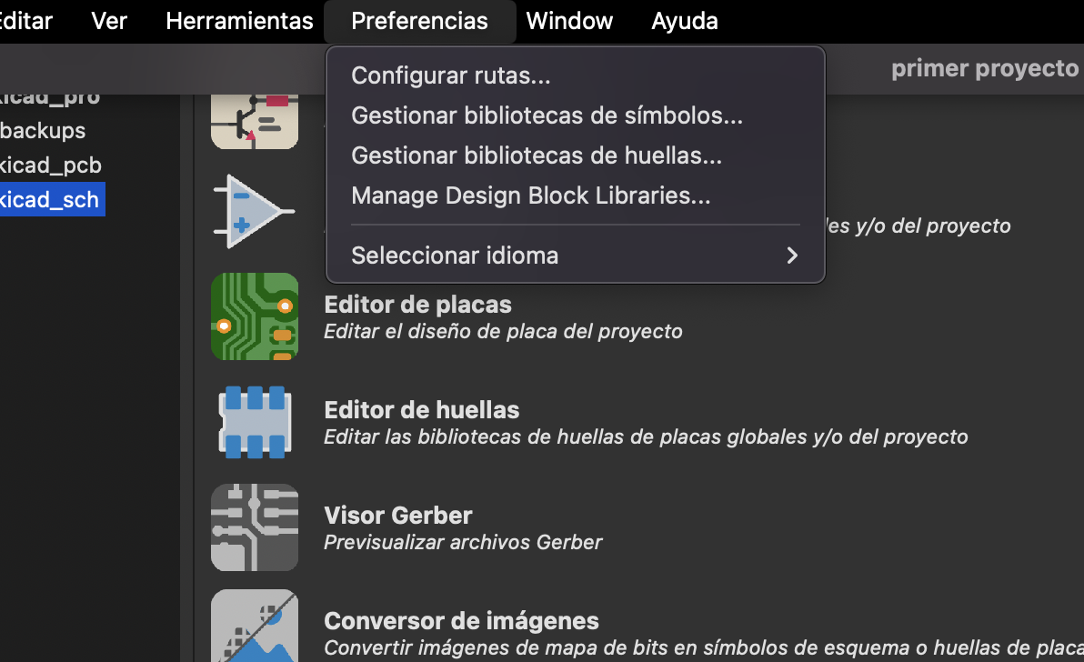
In this menu just click on the option with the library we want add and just follow this little tutorial.
Each "program" will have a different file to add, but everything on the same folder.
-
Symbol library
fab.kicad_sym -
Footprint library
fab.pretty -
Manage design block library
The hole "fab" folder
Yep, in every library the name of the new library in the app will be the same "fab" so we can identify it easily. Alright we are done with the pre. We are ready to start knowing what in this world makes each editor.
Now we are ready to start making project with kicad, you can repeat the process with any other library you have
Start a new project
Yeah, I have to write this down because even that is confusing.
Very easy, just click:
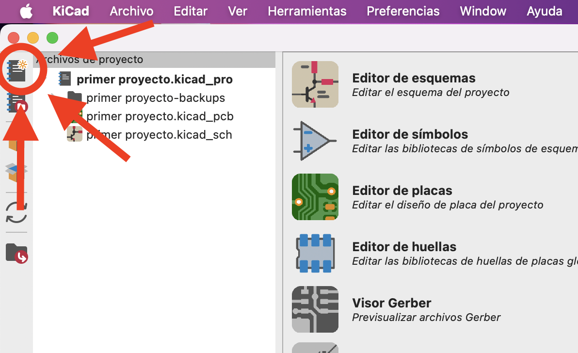
On that button, which, this will create 2 files a schematic editor and a PCB editor.
Be careful this two files are connected, don't delete anything or open anything directly from the finder folder, just open the kicad program and open those files
in the kicad program, don't move them, just edit them.
Perfect done creating a new project
Knowing the editors
Schematic editor
Every editor edits whats the name says jijijijijijijijijjijijijijijijijijijijijijijijijijiji
Besides the bad joke, what does that mean, well
The first one, literally the first option "schematic editor" I think it's in english, this one is to add and connect the components we will need for our project, like the micro controller, resistors, LED's, push buttons, capacitors, and everything. And it looks like this:
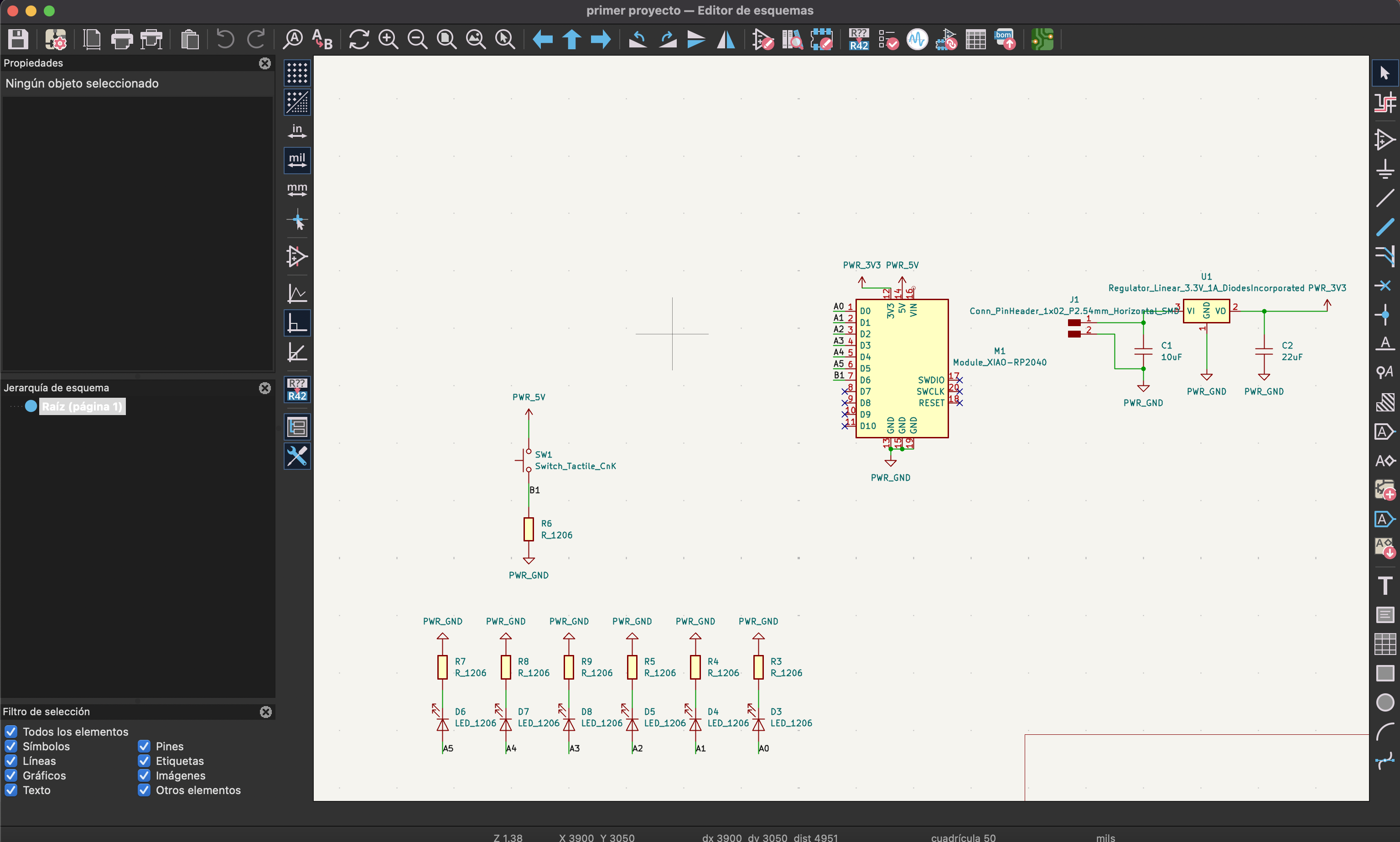
Here I have A LOT of things to explain.
starting with, here we will work with symbols for example the big rectangle in the middle with a lot of pins of the "schematic editor". This big rectangle is the symbol of a
xiao rp2040 micro processor, and so each symbol has a name which tells you what is it, "R" is for resistor, "C" is for capacitor and so on.
to add them to the circuit we have to follow the next tutorial:
Add components
On the right side menu the third option is to add a new symbol, click on it and the libraries will load, just for the first time because we added a new one. Then the
hole symbols menu will open, there is a search bar on the up left side of the window, just type the name of the component you want and it will show you all the symbols with the
name you typed divided in the different libraries you have, collapse them all until you find the "fab" library, select it and click ok.
the search window will close and the symbol will appear on the work space. you can select it ad move it around and with "R" you can rotate it.
Knowing this we can add some leds, resistors and and the micro controller and connect them with wires, just like in this video:
Connecting components
There are many ways of connecting components, the easiest, mor intuitive and first method is the following one:
This is a way of literally connecting the components between them.
The second one is to add a kind of symbols, and these are the power symbols. This ones are to connect the components with out wires, is like a bluetooth connection, IMPORTANT to remember if we want it to work properly, both symbols have to have the same name, if you change the name, it will not work. With this in mind you can separate the components on groups and not have a mess around the micro controller.
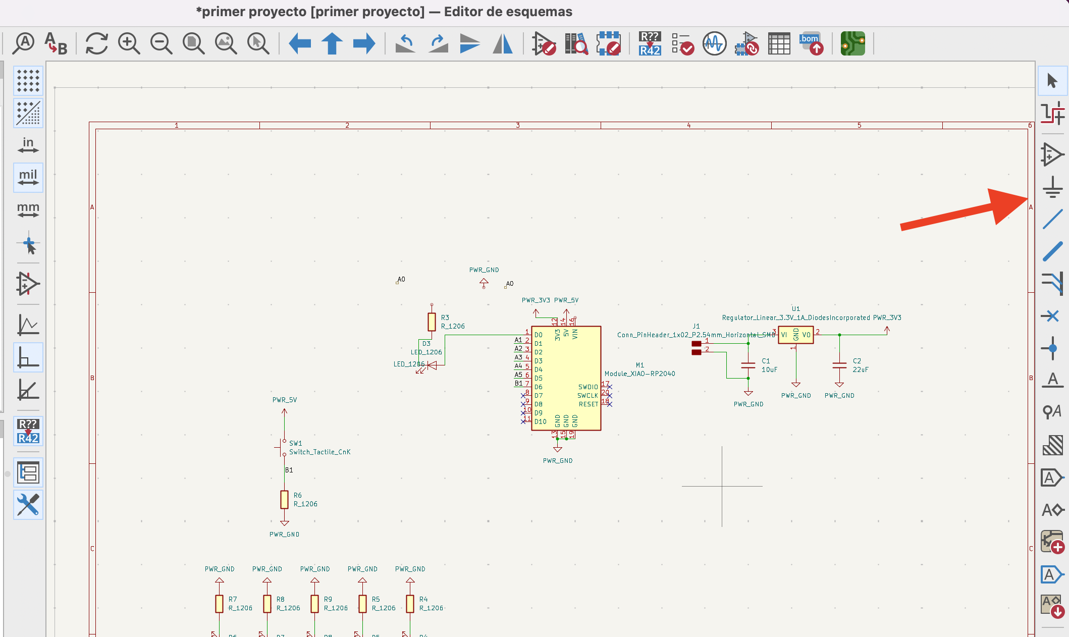
NOTE, the only ones I'm using are 5V and GND power symbols and those are just to power the components.
There is a third option to connect wireless in this program and it is adding Labels, you can create labels to connect the pins wireless, just make sure to give each pin a different name and duplicate the label to the component you want to connect so they both have the same name.
Checking connections
I though I was done, but I was not, I finished the connections and adding my components and everything ut guess what, there is a electronic rules control I have to run to make sure what I'm doing is ok, not good, not great, just ok. Let me introduce another video to show how to do this:
This will prevent me of doing an exploding circuit and lets explain the errors because this program doesn't think like we do.
Let me add a new diagnostic so I can explain something important.
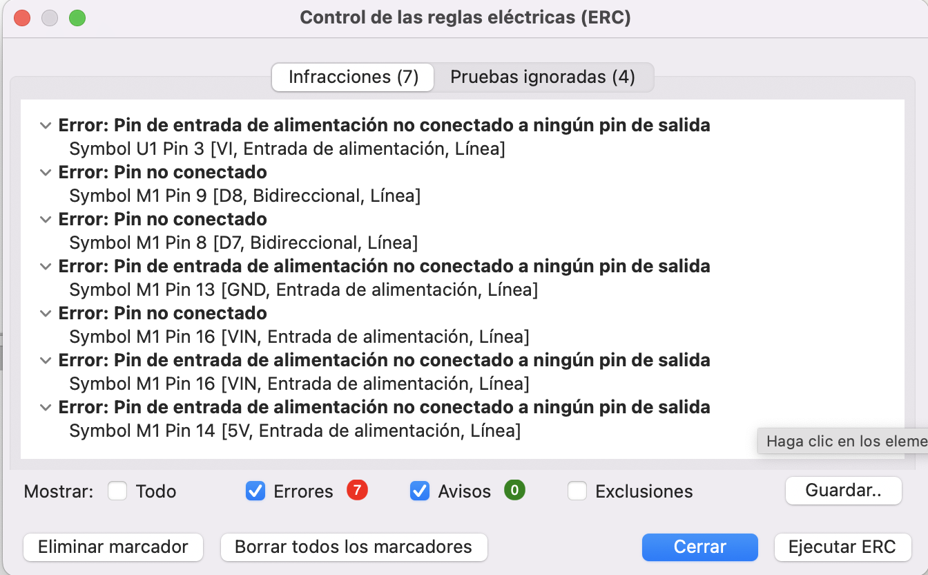
Within this errors we can see:
- input power pin not connected to a output power pin
- not connected pin
- And that's basically it
This kind of errors are because the program is not reading some things that we have already contemplated physically. And because we are not using those pins or I do forgot to connect those pins. We can just added a pinhead and that's it.
Which are the values of the components
The capacitors are 10uF and 22uF why?, because the data sheet of the component we are using says so
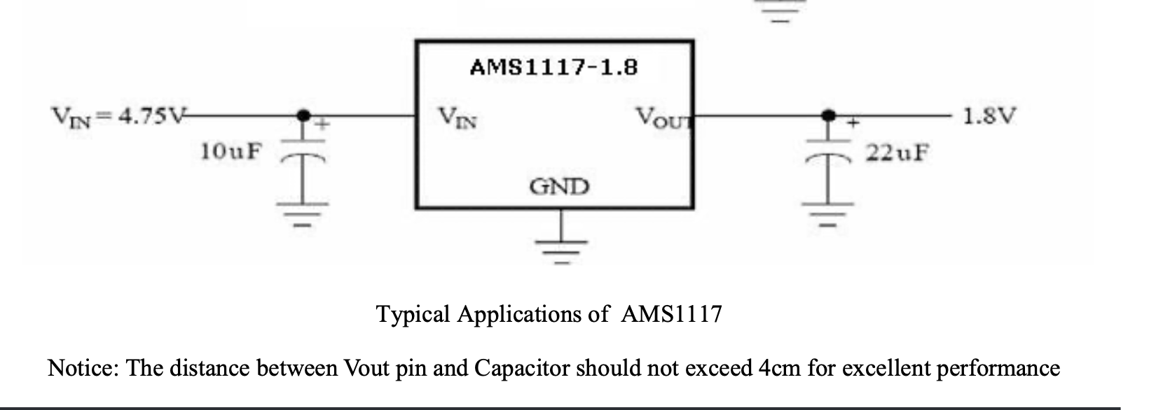
and the resistor I use this graph to know how luminous I wan the led to be and applied ohm's law
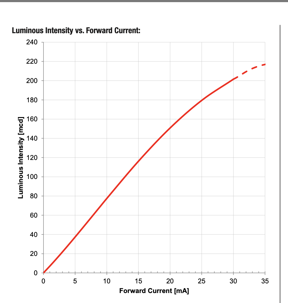
I want it to have around 120 luminous intensity, so I will need 15mA (0.015A), the pins of the xiao gives 3.3 V output soooooo.... R = V /I = 220 ohm
Thats basically what you have to know about this first editor, if you want more you can watch You Tube tutorials jijijijijijijijijijijijiji
PCB editor
Open the PCB editor
The PCB editor is creating the circuit as it will be physically. To access to this window, on the Schematic editor go up and click on the green button to directly open the pcb editor of the project. Just like in this image:
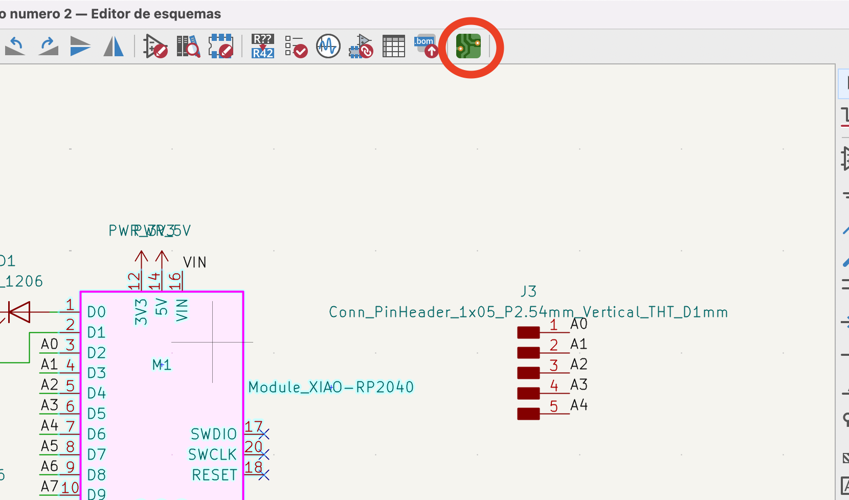
A hole new window will open and it will automatically add the components you added on the schematic editor. You have to place them and put them how ever you want.
Starting
But first we have to set some default parameters/rules for the pcb connections like the minimum space between traces, the thickness of the traces and many other rules, but the important, and with what we will be working are those 2. Let me take a video that will explain you where and how, just follow the mouse:
For this first project the teacher told me to set the trace thickness at 0.8mm and the minimum space between traces at 0.4mm. Of course these parameters can be smaller but as is my first circuit and I will have to solder the components, it sounds like a great option.
Knowing the interface
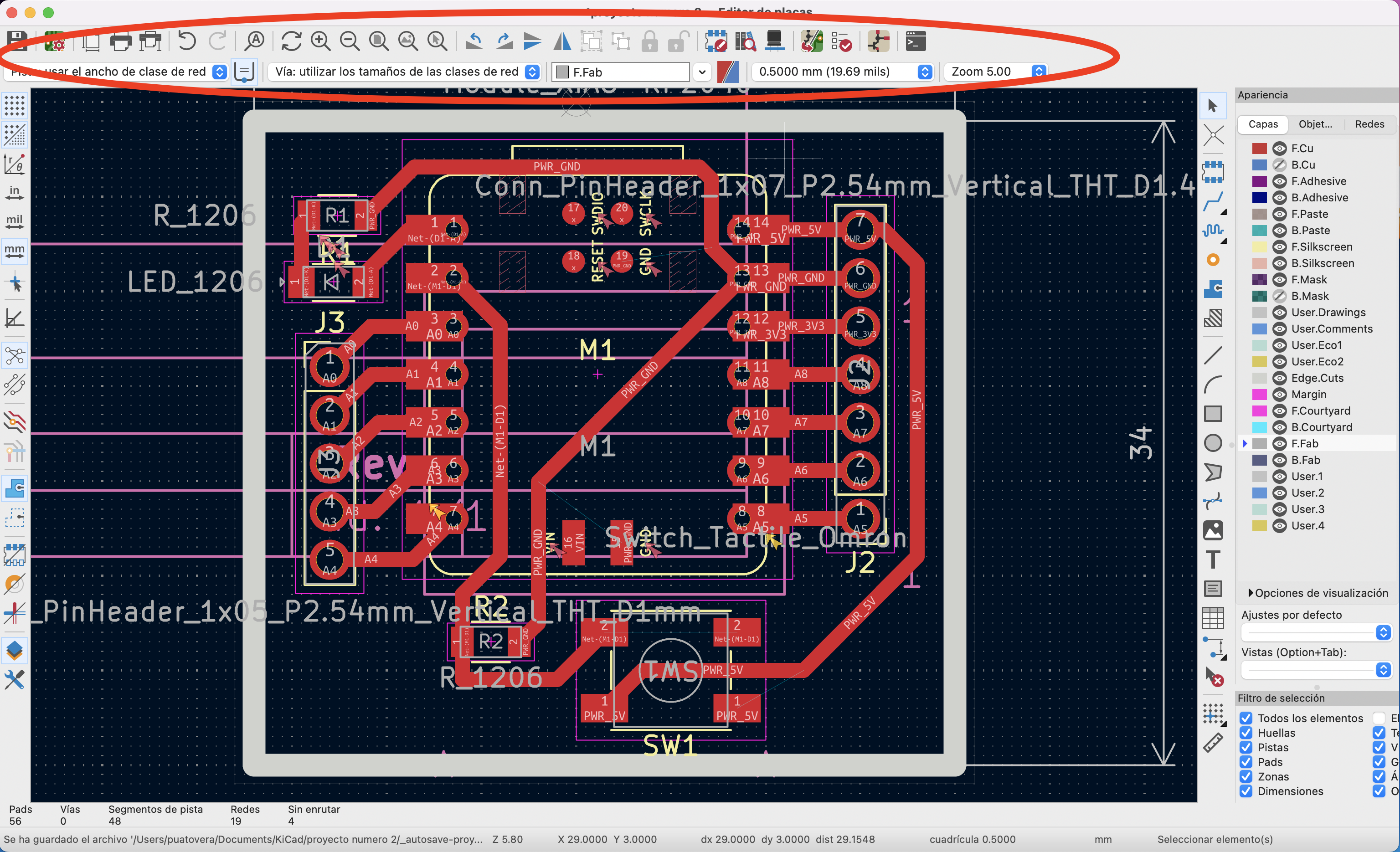
Now let's meet the interface, this interface has tools on the upper side, the left side, the right side, and the very right side of the window.
On the upper menu we have some quite important tools like, rotate, mirror, upload form schematic, run the design rules, and open the schematic file.
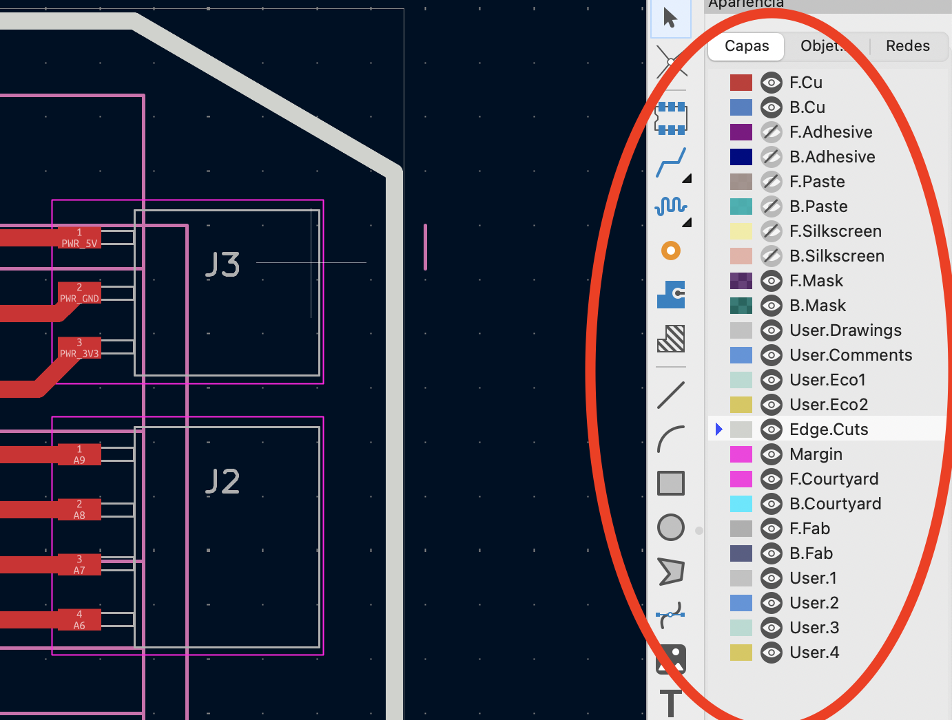
On the Right side menu there will be most of the tools we will need, tracks, figures, and layers. I have to explain something on the layers, as you can see on the name, each layer refers to a different process
of the circuit, the first layer, F.Cu means, Front Cu (coper), this layer is for the coper tracks and it's color is red, so the front tracks will be shown in a red color.
The next layer is: B.Cu from Back Cu, and it is for the back side of the plate, but in our case we will not be using it. There are many other like, adhesive, paste, mask and so on.
But we will not be using them as well. But we need to for "Edge cuts" and "user", As the name says it, the edges will be in it's respective layer, and we will use the user to create the holes, in case we need them.
Creating tracks
Now, as we already gave the program the rules for the tracks, we can start creating them. This tracks will be the coper lines that will connect the components. for this we just have to follow the video:
NOTE this tracks will be according to the predefined rules and th given rules.
Make sure to change the layer and once done, we can select any figure tool and make the edges of our circuit.
That's for the pCB editor
Running the rule design checker
The rule design checker does exactly what you think it does, check that every rule is followed, and if not it will show you an error or a warning.
Let's analyze the warnings and errors I had.
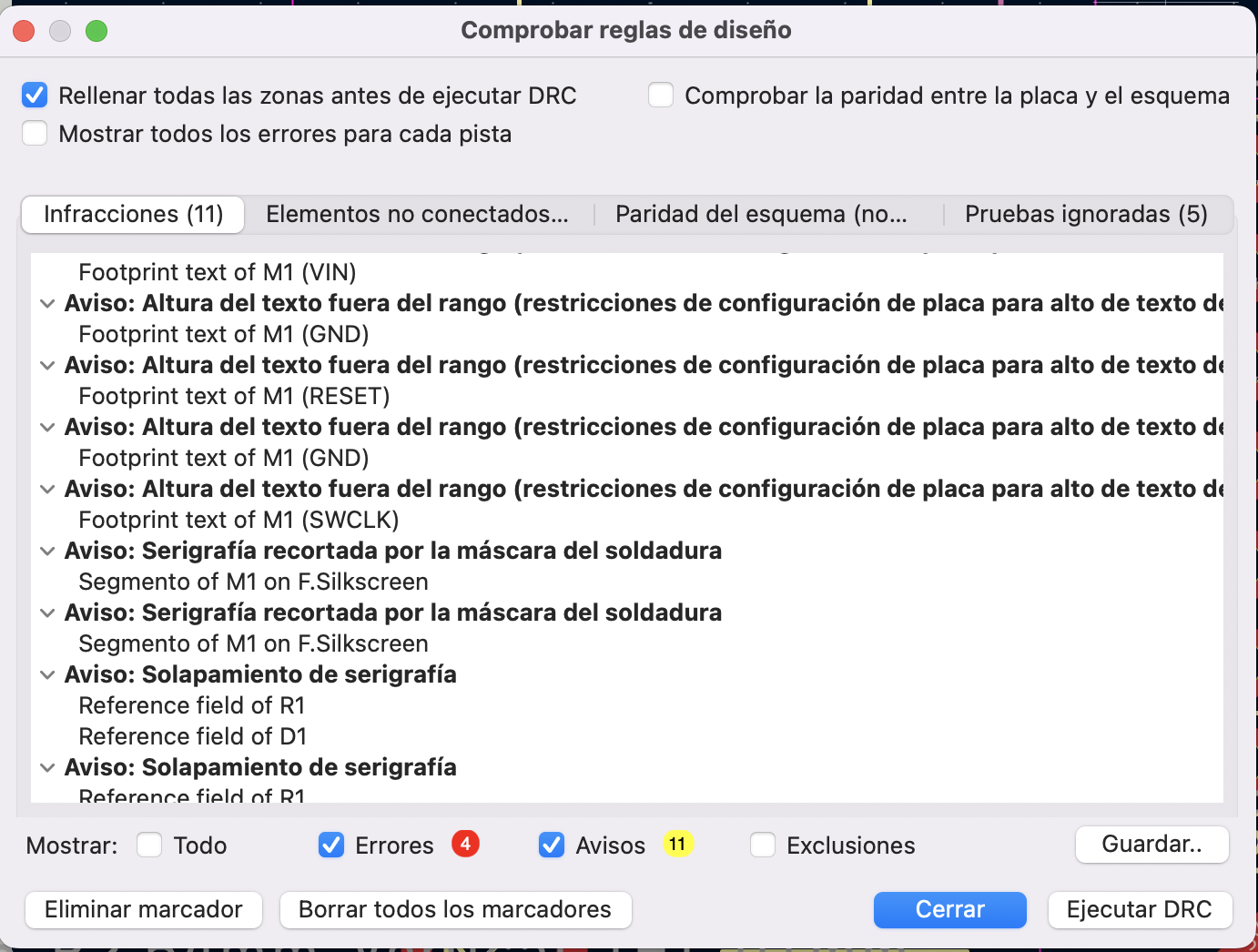
The first thing to appear are the warnings, these ones are mainly a text over another one or a text that goes out of the edge or something related to the labels of the components, In our case we can ignore them because we will not work with labels, but in case be had to work with them, then we have to look for this warnings. The second page/section are the errors
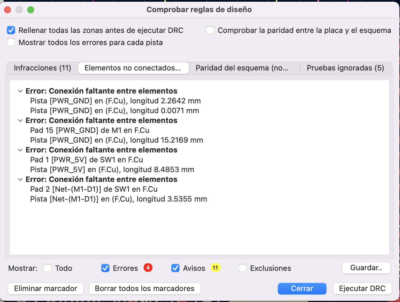
In this case are non connected pines like the buttons pins and some grounds. This might sound something to worry about, but in our case we can also ignore them, because we will not be using them. They can be not connected to anything and it will be ok.
Calculator tools
KiCad has a calculator for this kind of projects to make your life easier, it has many programs but in our case we will be using just the "track With" calculator to know the minimum required with.
-
Access the calculator
-
The track with program
-
How to use it.
The calculator will ask us to enter 3 parameters-
Current (I)
This is very intuitive, the current we will be working with -
Temperature rise
This one refers to the temperature we are considering to work with, because every electronic circuit gains heat while working and we have to contemplate it in this design. So the maximum temperature we expect. -
Conductor length
As the name says it
-
Current (I)
- The results will we shown on the right side of the window, we can copy the value and paste it on the parameters of the rules design of our project.
NOTE, the result was quite thin, about .3 mm, but solder those tracks was going to be very hard, so our teacher told us to set them at .8mm so we can work easier.
We are finally done :)
What I did
This is my first tim doing something like this so, honestly I just copied what my teacher did and made some minimum changes.
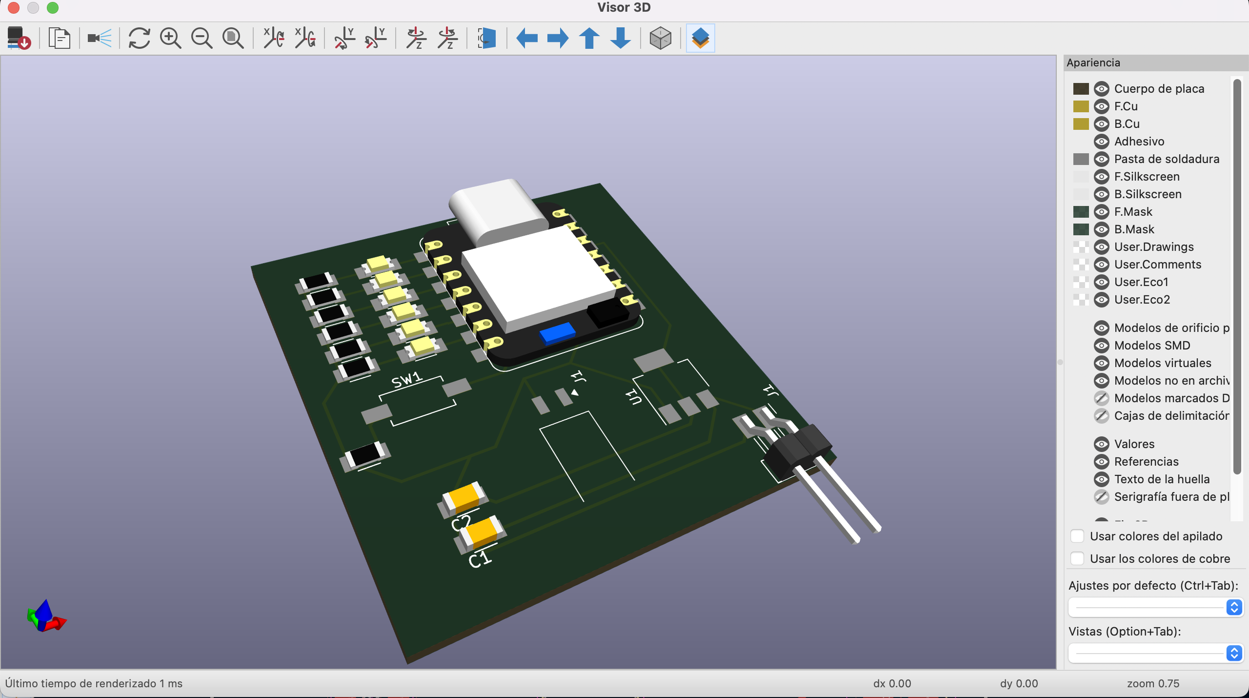
The files
What I learned
This become easier as more as you use it, but this first time was quite confusing, but it might be because, once again, I left it until the last day JAJAJAJA. Other thing is that I thought it was going to be even more difficult, but this program has a lot of tools that make this process easier and saves you a lot of time doing calculus and stuff like I did in the University.
Notes for my future self:
-.- nothing to say, Ahora no quiere funcionar esto, quiero llorar