Electronics Design
Dripping water can penetrate the stone. — Proverb
ZB FAB Academy W06 Planning/Documentation
- Thursday 2/27/25 EOD: Complete group assignment with AB/NS/KH going through the testing equipment in the FABLab. Minor updates to previous pages
- Requested Working Time: 60-90mins.
- Requested Help: Need guidance from AB/NS/KH on use of different testing protocols at some point before EOD Thursday
- Friday 2/28/25 EOD: Complete Documentation for KiCAD walkthrough that has already been accomplished/finished
- Home working time
- No necessitation of PAST visit
- Saturday 3/1/25 EOD: Complete design for a potential final project board through KiCAD
- PLEASE take screenshots as you go for documentation
- Home working time
- No necessitation of PAST visit
- Sunday 3/2/25 EOD: Finish any unfinished work on previous weeks’ assignments
- Home working time
- Potential necessary in Office Work to finish Laser Cutting/XTool board Engraving/3D Case printing
- Monday 3/3/25 EOD: Hopefully print and potentially solder designed board (assignment for later week); Additionally have at least 50-75% of week’s documentation done and uploaded to Repo for meeting Tuesday; Print pase for KiCAD designed board during working hours
- Requested Working Time: 90-120mins.
- Tuesday 3/4/25 4PM: Finish uploading Documentation to Repo/Tie Loose Ends before Meeting with Ohad/Group
- Requested Working Time: 60-90mins.
Reduced Process This Week:
- Download KiCAD and FAB libraries
- Use KiCAD tools to design the schematics and PCB layout
- Use the KiCAD viewer to look at a rendering of your PCB
Tasks This Week:
Group assignments:
- Use the test equipment in your lab to observe the operation of a microcontroller circuit board
Individual assignments:
- Use the test equipment in your lab to observe the operation of a microcontroller circuit board
- Use an EDA tool to design a development board that uses parts from the inventory to interact and communicate with an embedded microcontroller
- extra credit: try another design workflow
- extra credit: design a case for it
Below, I walk through some of the notes/screenshots that I have from my work this week and explain my thought process as I was completing my assignments.
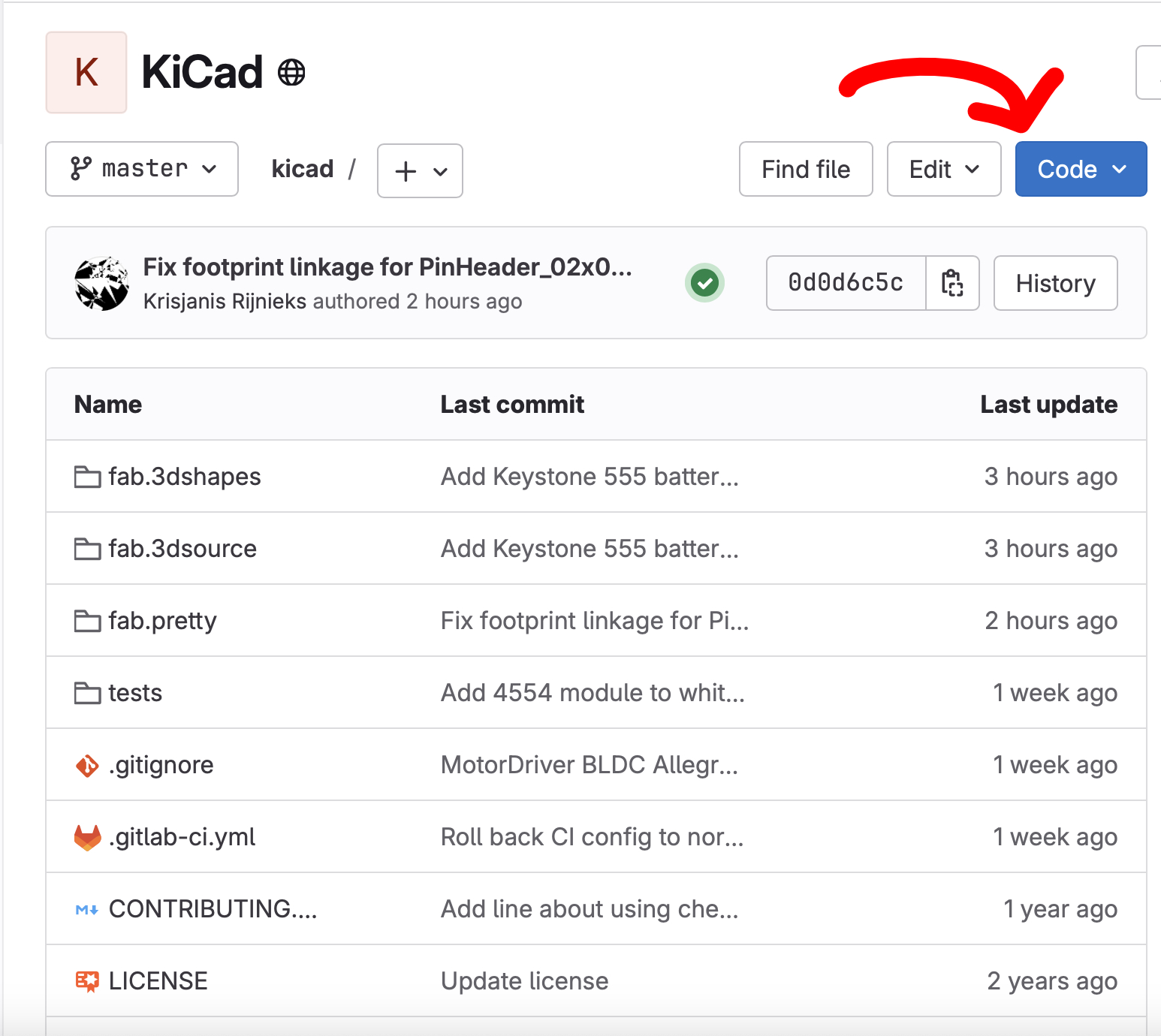
- Dowload KiCAD (Version 9/Latest Version if possible, to avoid issues recitfying libraries later)
- Download the libraries from FAB Academy for the specific footprints and symbols used in FAB
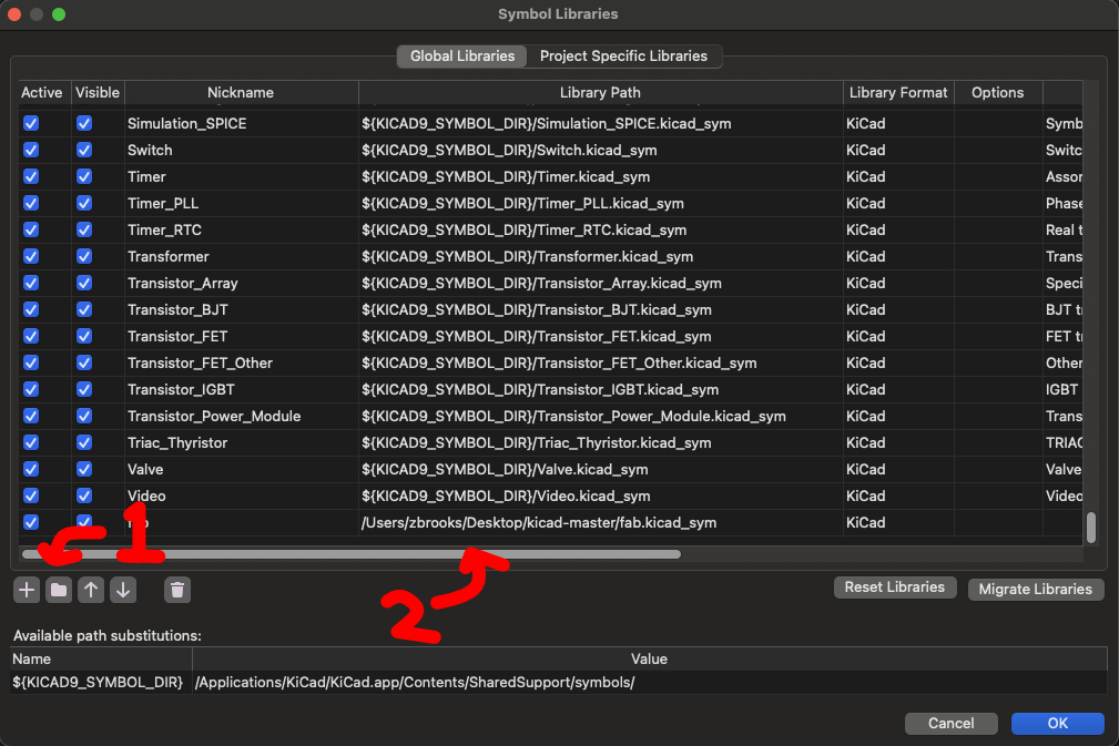
- Open KiCAD and go to Preferences -> Manage Symbol Libraries and add the symbol file from the FAB github. Unless changed/updated it should be named something like "fab.kicad_sym"
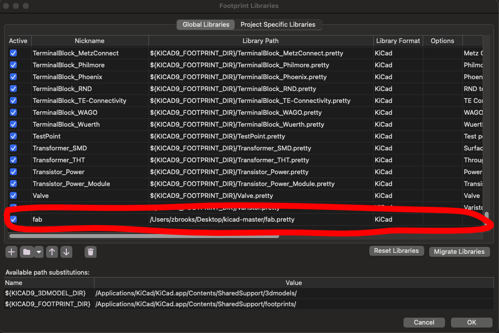
- Follow the same process for Preferences -> Manage Footprint Libraries. There should be a file with a .pretty extension which can be used in place of the folder above
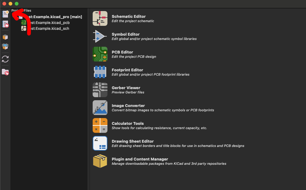
- Create a new file
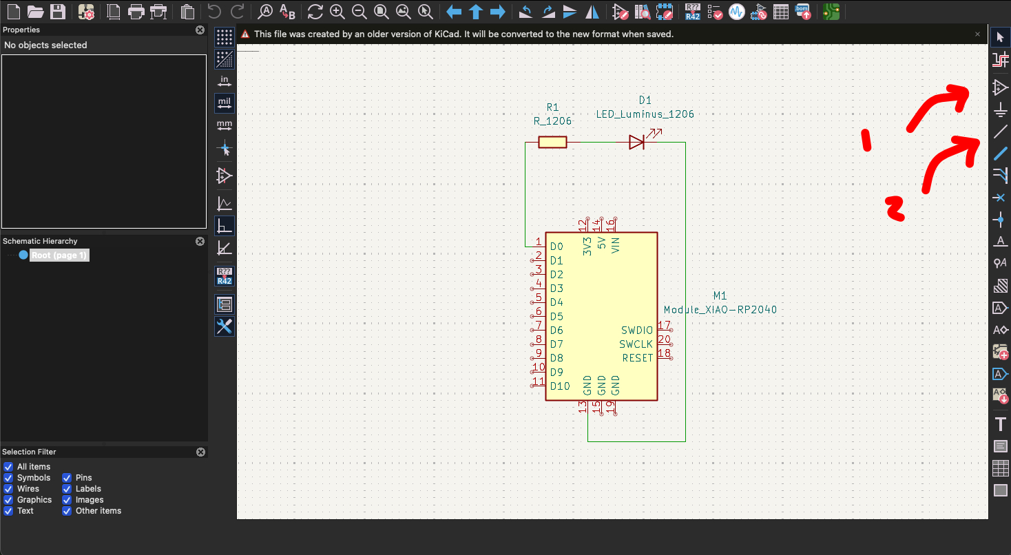
- Enter the Schematic Editor and use the tools labeled 1.) and 2.) to place your symbols and connect them using wires
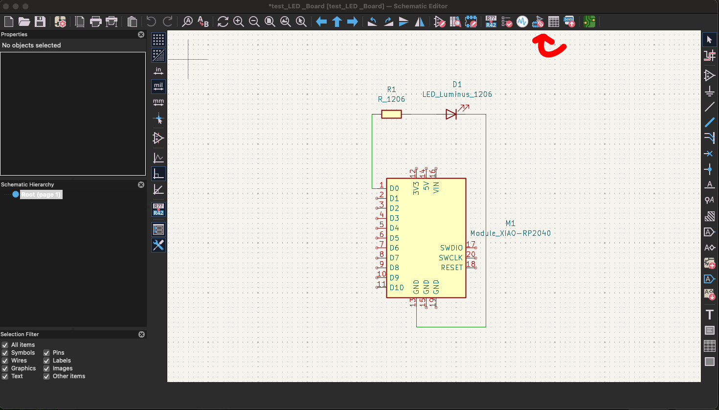
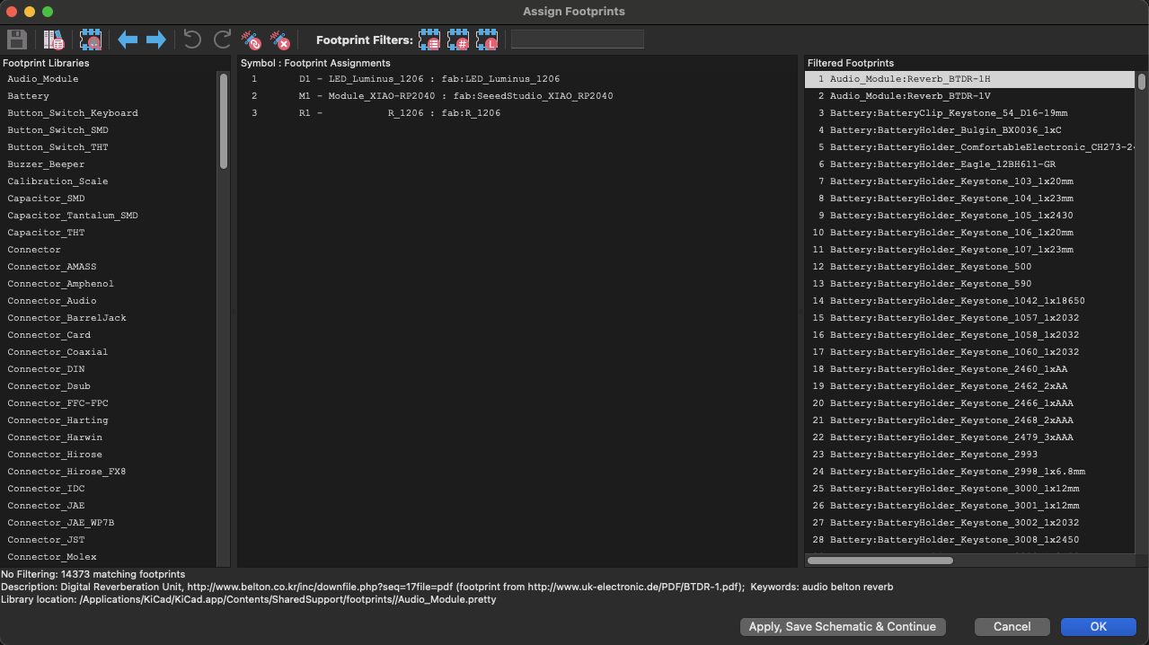
- Make sure that all of your symbols are assigned to footprints using the "Assign Footprints" tools
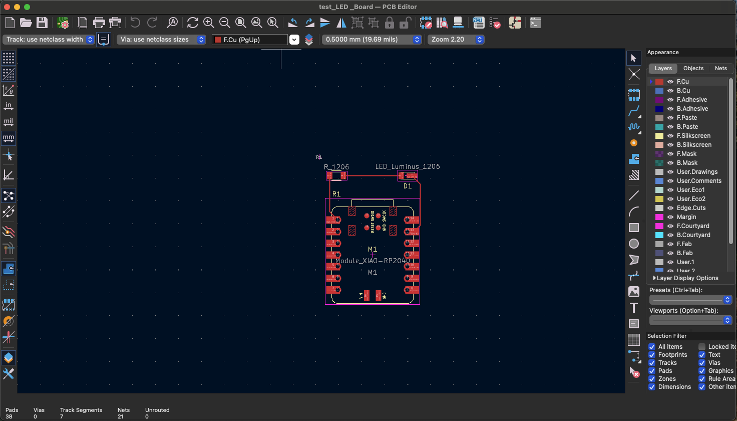
- Open the PCB Editor and go to Tools -> Update PCB from Schematic
- This will create a jumbled mess of components. Seperate them, and connect them using the path tool to create a final product that can be used to create a millable PCB
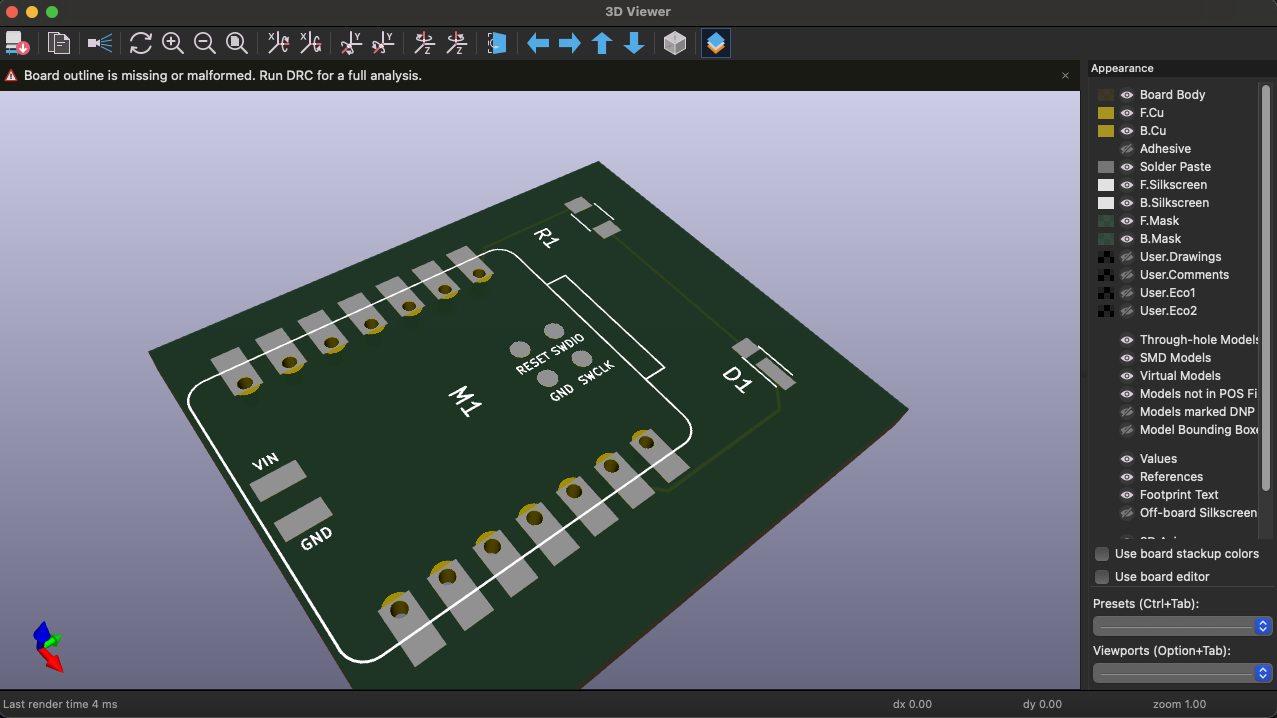
- To view the PCB in a 3D Render: In the PCB Editor, go to View -> 3D Viewer
- Using the Multimeter for continuity
- Turn the multimeter on to the resistance setting
- Put one of the probes on the outside/ground of your milled PCB
- Put the other probe on the pads of your PCB and check to make sure that current can run from each part of the board that is connected to each other, and that there are no leaks
- Comparison Table for RP240 and SAMD 21 (the two available microcontrollers at my Lab) from W04
RP 2040 SAMD 21 Architecture ARM ARM SRAM 264 KB 32 KB OS Not Applicable Not Applicable Clock Speed 133 MHz 48 MHz Number of Cores 2 Not Applicable Flash 2MB 256KB Compatible Languages Micro/Circuit Python, Arduino Micro/Circuit Python, Arduino Pins - 11 Digital
- 4 Analog
- 11 PWM
- 1 I2C
- 1 UART
- 1 SPI
- 1 SWD
- 11 Digital
- 11 Analog
- 10 PWM
- 1 DAC
- 1 I2C
- 1 UART
- 1 SPI
- 1 SWD
- One of the biggest improvements that I would make to my workflow this week would be to start with KiCAD 9 and not have to update it. As mentioned below, making sure I have the right libraries was one of the more frustrating parts of the week, so not having to update mid week would've been very helpful
- This week I also tried to have better naming conventions for my images so that when I go to upload them, I have an easier time finding them.