Week 8: Electronics Production
Group Assignment (link): characterize the design rules for your in-house PCB production process and submit a PCB design to a board house
Individual Assignment: make and test a microcontroller development board that you designed
This page has the following sections:
Group Assignment Reflection:Getting Started / Introduction to Rolland Milling Machine:
Milling Work-Flow:
Soldering:
Testing the Board:
Hero Shot:
Other PCB-making machines - X-TOOL!
Files
Group Assignment Reflection:
In this week's group assignment we investigated the design rules and PCB process of our lab's Rolland milling machine. We were carefully taught it's operation and tested the different bits that would facilitate the tracing and cutting of the board.
We did a series of tests to determine the width of traces and the gap between traces that different bits in our milling machine would allow. This directly helps us to make sure our design is feasible, since the design will be produced by a machine with tools, and it will have limitations.
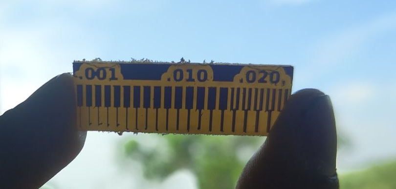
With the 0.8 mm bit it was easier to determine the minimum gap required between the spaces, however with the V-bits that was a bit more difficult, and while there is a calculator for that within Dr. Neil's mods, we basically determined that by experimentation.
Getting Started / Introduction to Rolland Milling Machine:
There's a few ways to create a design board in the lab, first way is with a Rolland Modela MDX-20 3D Milling Machine. Details can be found from the manufacturer here. Anyway, here's the set-up:
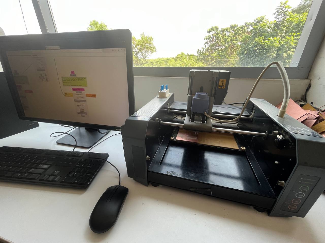
Actually this machine can be used for different purposes, but we will use it for this purpose. The basic idea is that we start with a board with a very thin piece of copper and the machine will mill (subtract) and remove portions of that copper layer, leaving traces, portions that are connected. The copper traces essentially function as wires in this way.
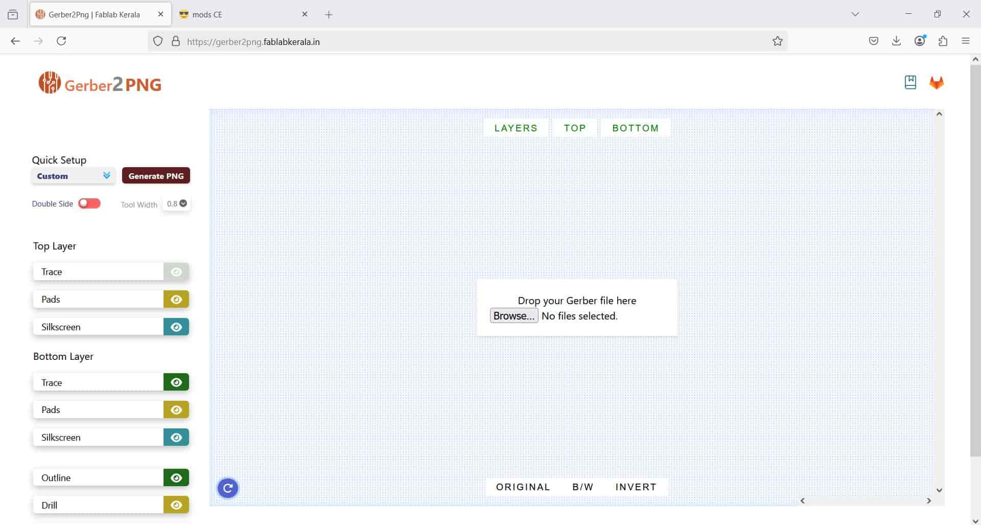
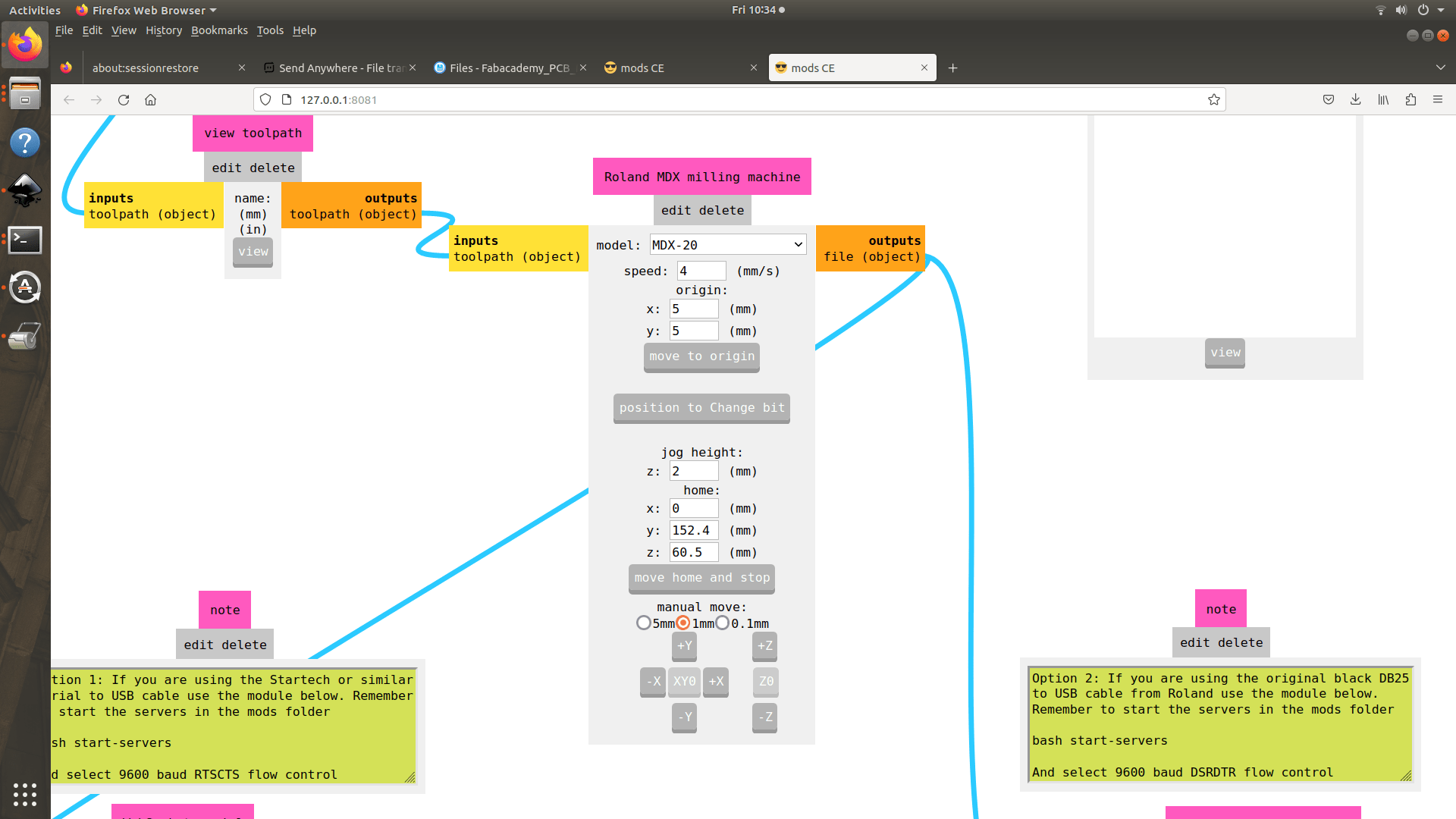
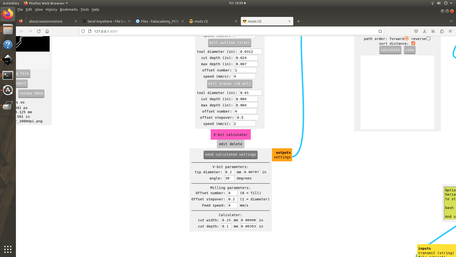
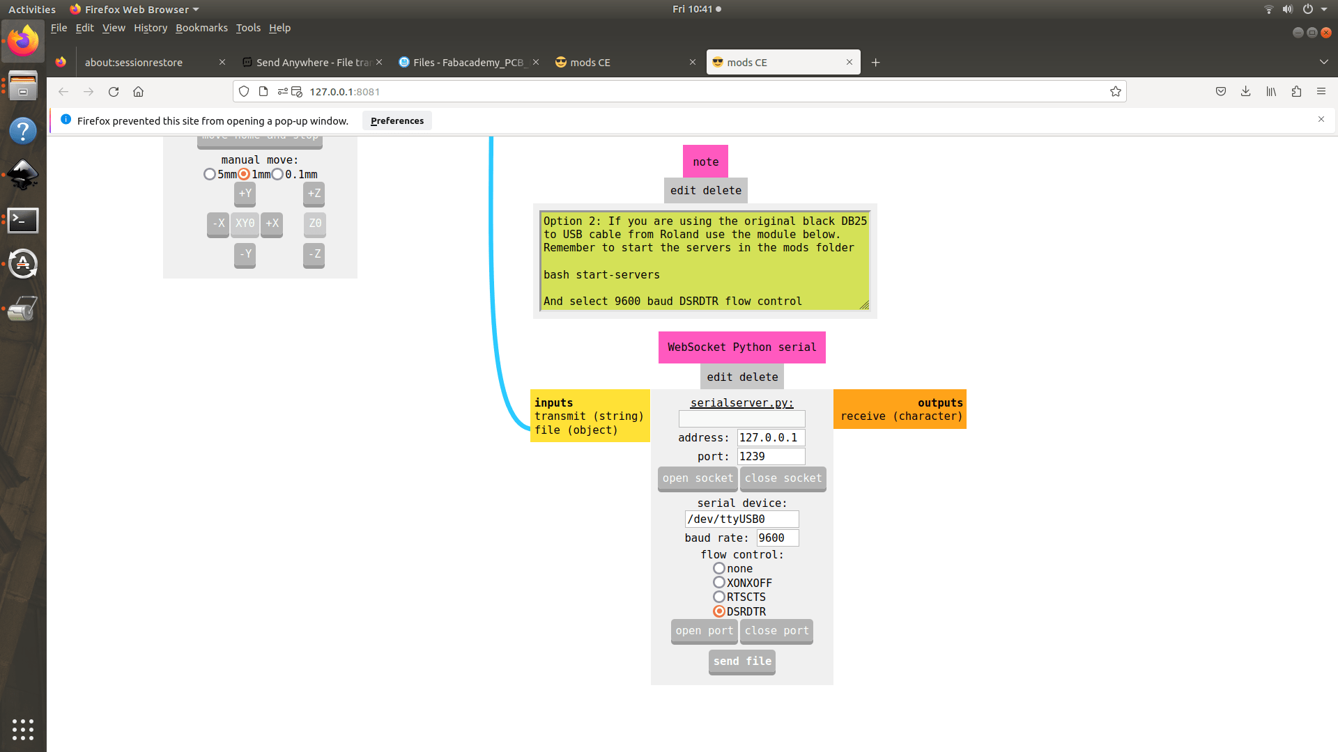
For software the Rolland milling machine uses Dr. Neil's Mods software which we also used for the vinyl cutter. This is quite convenient for us, all that is necessary is to convert our design files into either .png or .svg since these are the possible input file formats. To do this we will use a conversion tool developed by our very own Saheen. Here's the process:
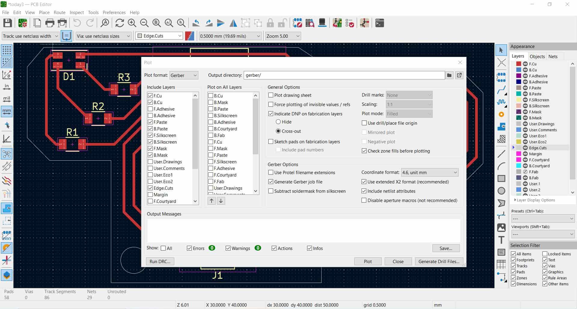
1. In KiCAD, open PCB Editor, then output as Gerber. Plot, generate drill files, and save to folder. There will be about 10 files.
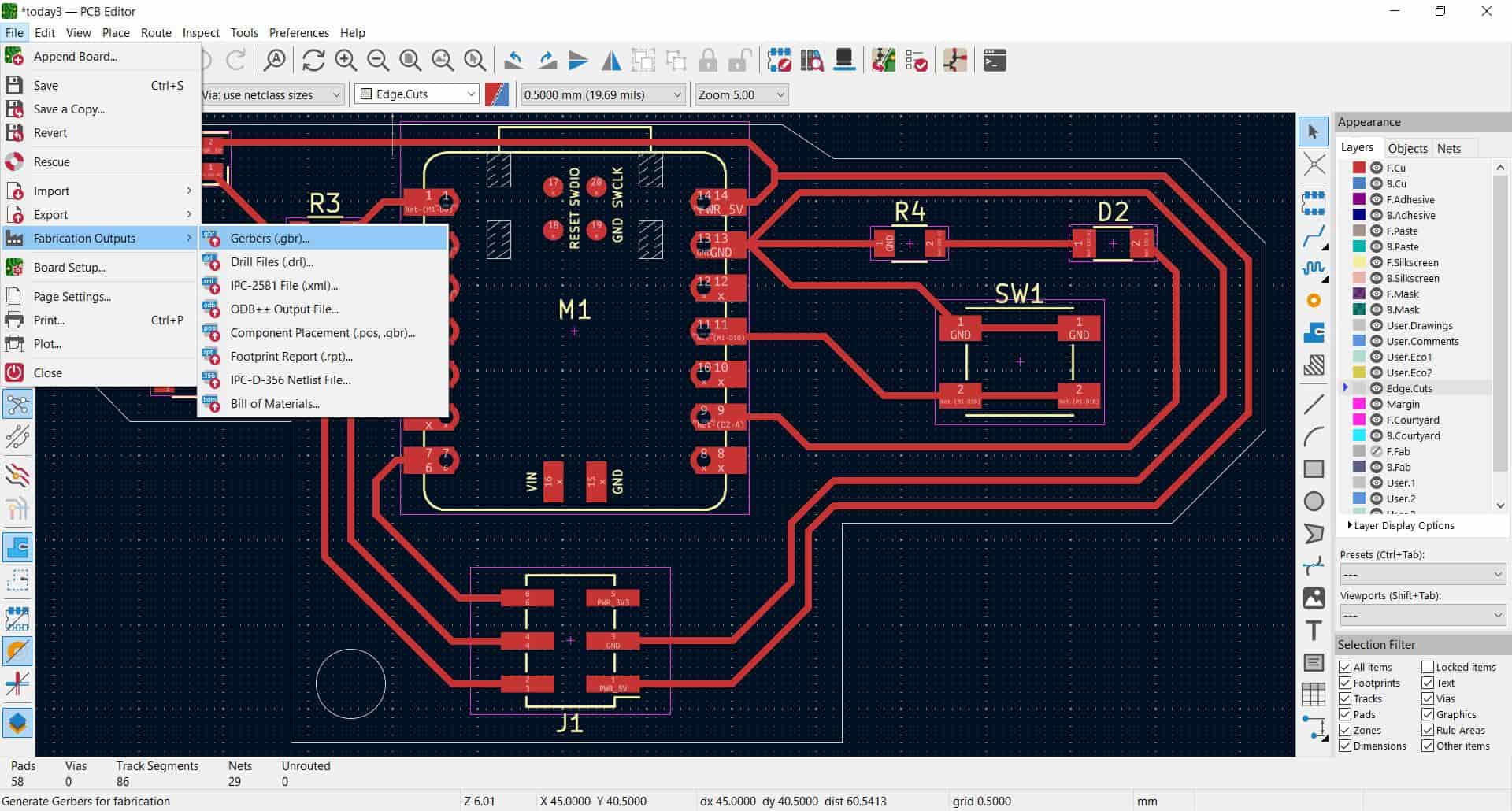
2. Go to Gerber-2-PNG, drop your files and save the outputs.
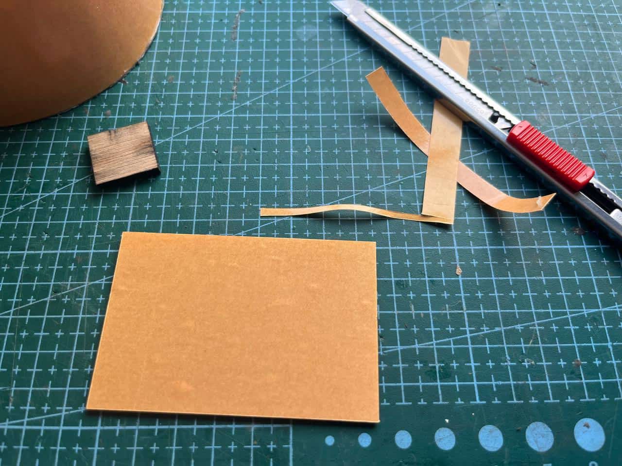
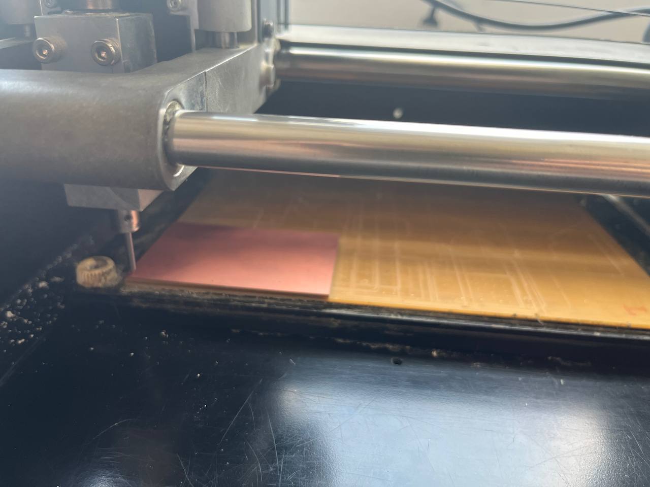
3. The last part of setting-up is to take our 2"x3" copper-plated board, put sticky tap on the back and put in position.
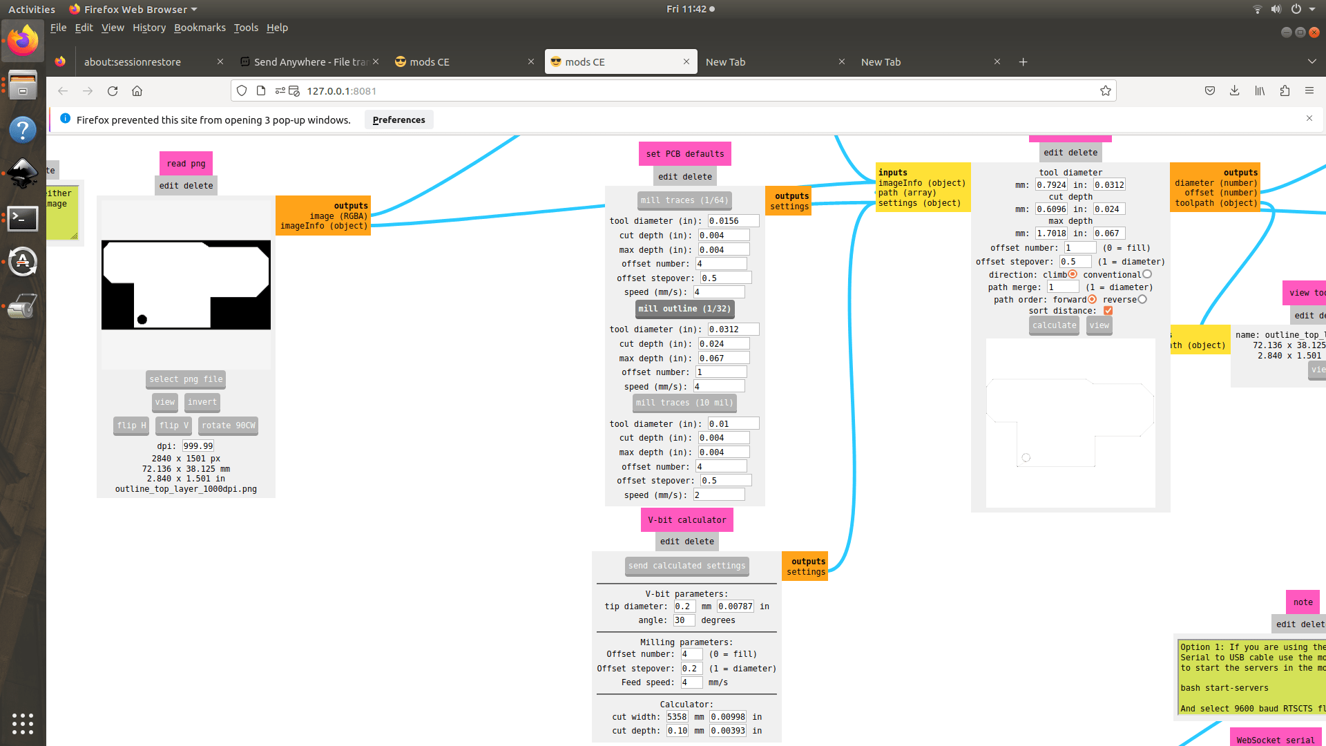
Milling Work-Flow
Go to Mods (on the computer connected to the Milling machine) to continue the process. Note that we go to local version of Mods because there Saheen has added a feature for positioning the gantry to make changing the drill bit easier, as seen below:
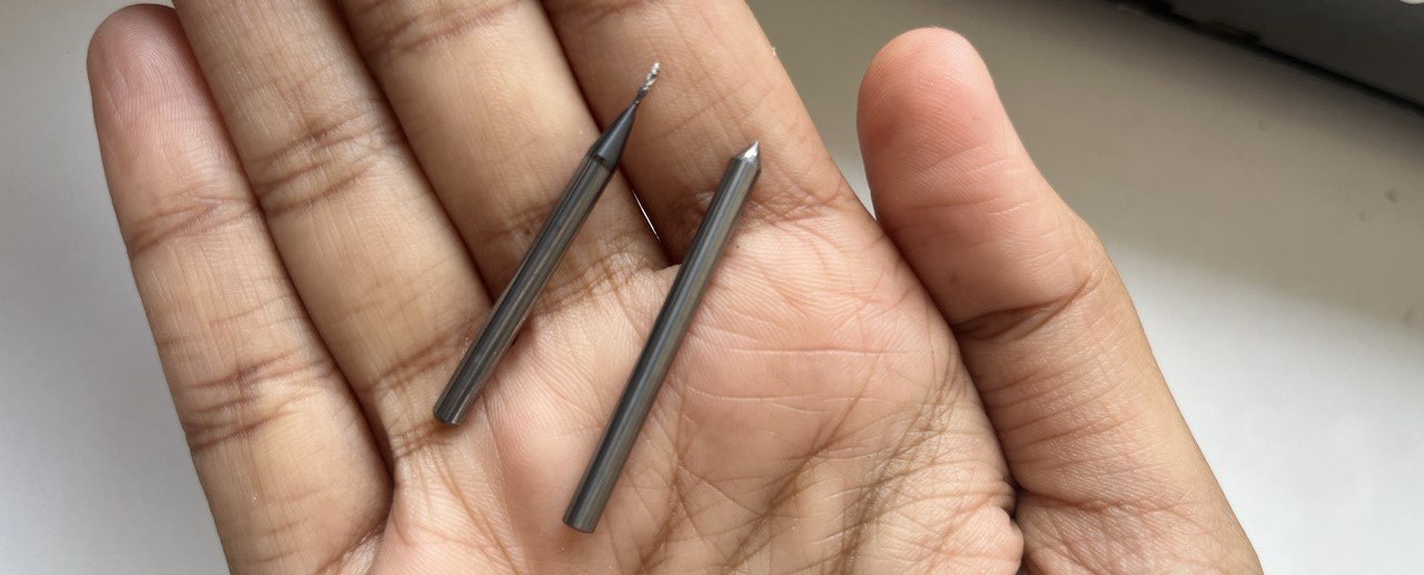
There are a variety of different bits. For engraving we will you a V-bit with tip width 0.2 mm and a 30 degree angle. For cutting out the PCB we will use a 0.8 mm bit. They are both shown here in Ancy's hand:
Engraving
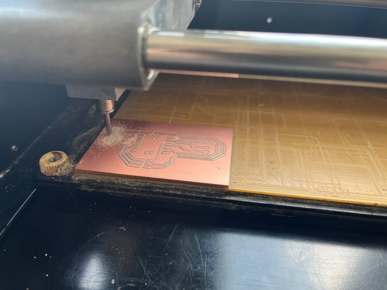
So we will start with engraving, and for this we must review the V-bit settings. Although the copper layer is 0.07 mm think, we're gonna set the cut depth setting at the very bottom to 0.1 to ensure that the entire layer is cut. If not, there can be traces connected which can short-circuit the electronics.
After sending the calculated settings, calculating and viewing the tool paths, we can now send the file and the machine automatically starts.
Here's a short time-lapse showing the process:
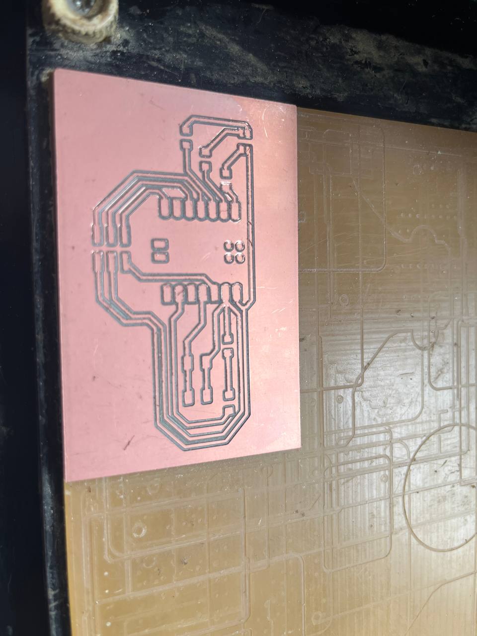
Unfortunately when finished, some traces were not cleanly cut out. So we cut it again, but first we lowered the tip head just a tiny bit at the origin position when we were leveling in the Z-direction. And the result the second time was fine:
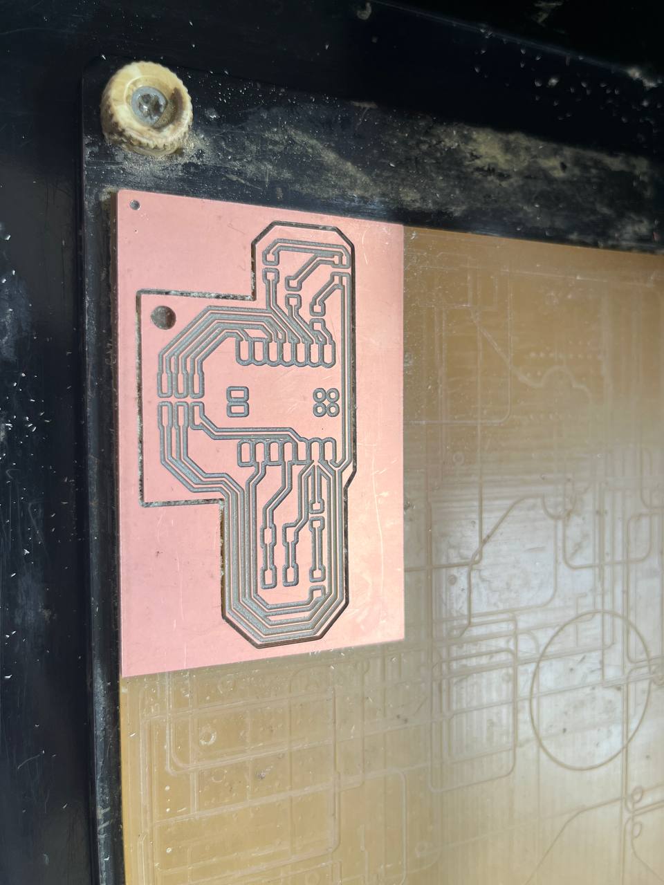
Cutting
Now it's time to cut out the outline of the PCB. For this we changed to a 1/32" (0.8 mm) bit, loaded the outline .png file, calculated that and started!
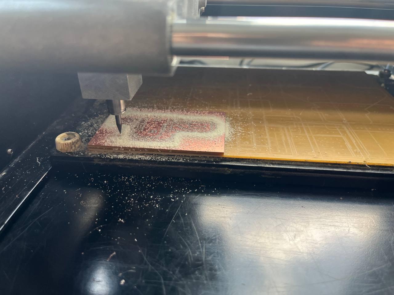
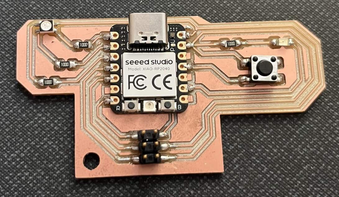
Ma sha Allah!! Here's the cut-out of my very first PCB:
Soldering:
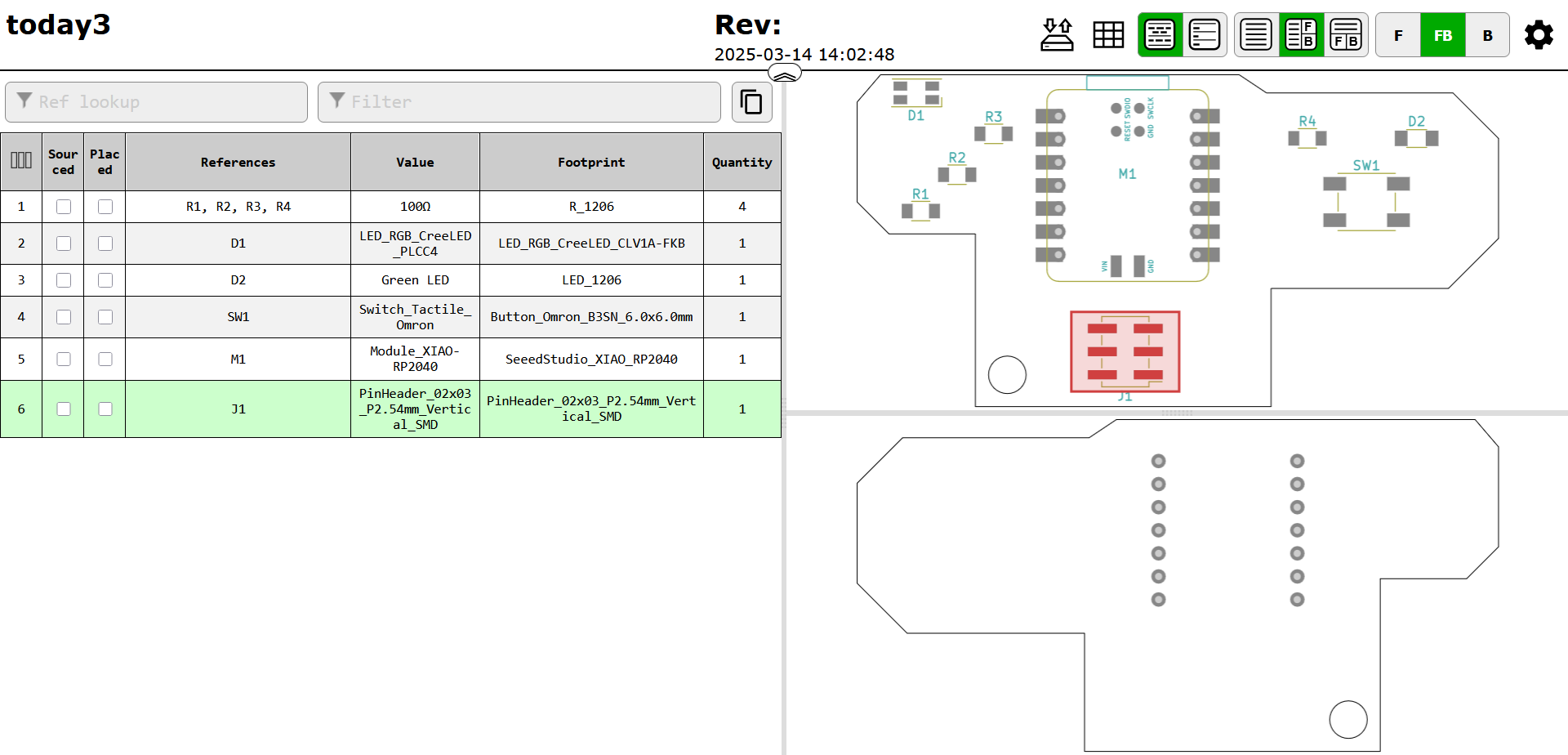
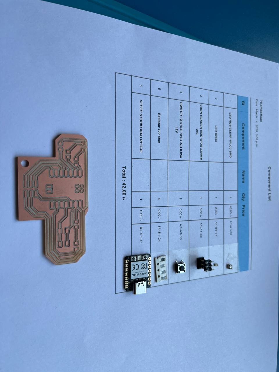
First we need a BOM (Bill of materialS) for our individual PCBs.
Within KiCAD we can follow these steps:
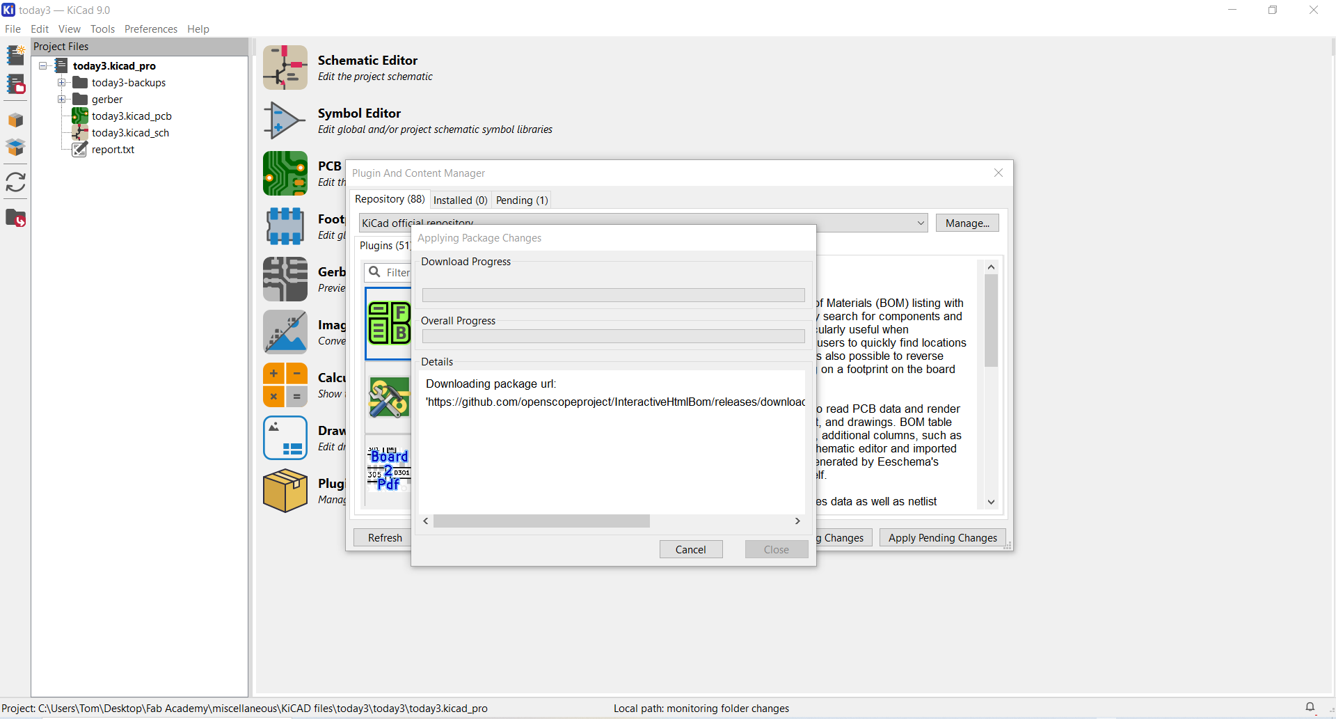
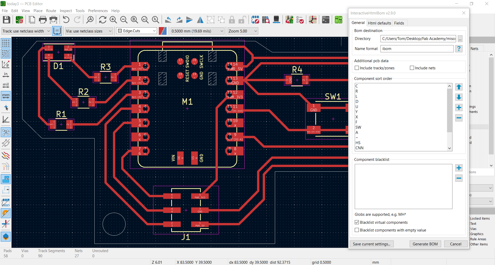
Finish the process by clicking "Generate BOM" and we have our list of materials to Solder!
Next step is to gather the pieces. In Fab Lab Kerala we have FabStash which allows us to select the items we need and place an order for them!!
Anyway, we are responsible for selecting the parts from the highly organized supply room:
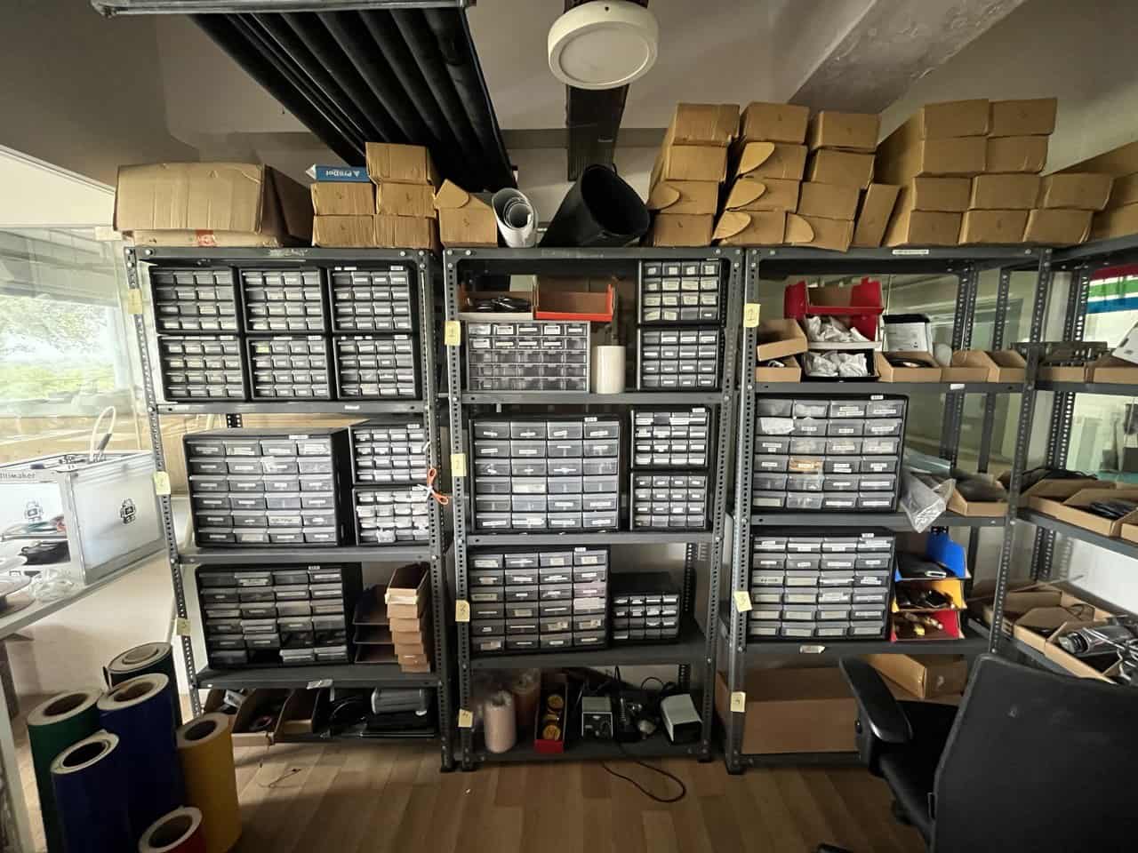
We selected all the parts...
Here is our set-up, with air filter on the left, soldering iron and hot air gun on the right:
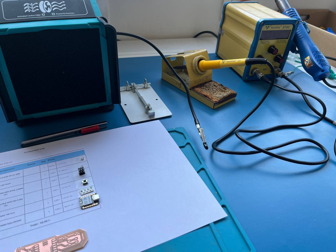
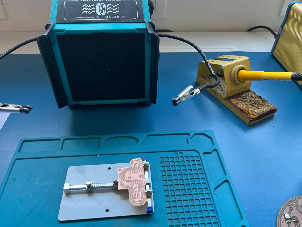
We put the board in a clamp to keep it stable. Underneath is a mat which is resistant to the soldering iron.
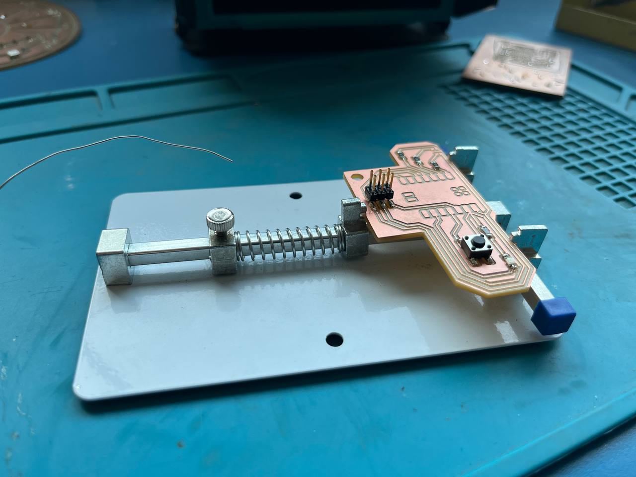
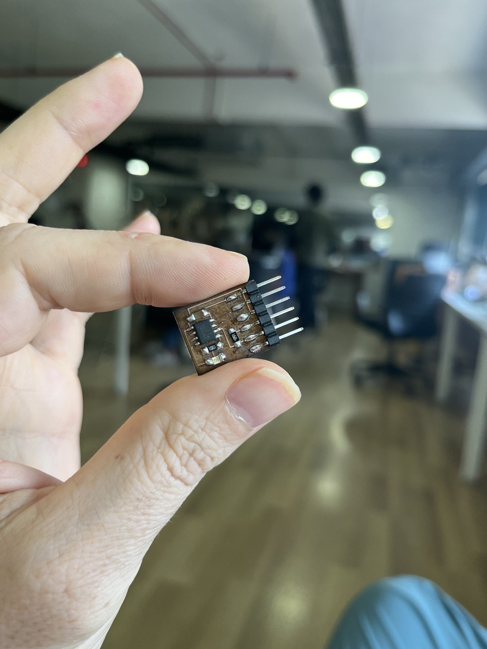
This photo shows the board half-soldered. I should not have put on the pin-header so early. But so far so good.
Here is the finished product. Although it's simple I'm very proud because I did it all myself and it works.
Big thanks to Saheen for his support; he carefully gave detailed instructions and advice for soldering in the most precise way.
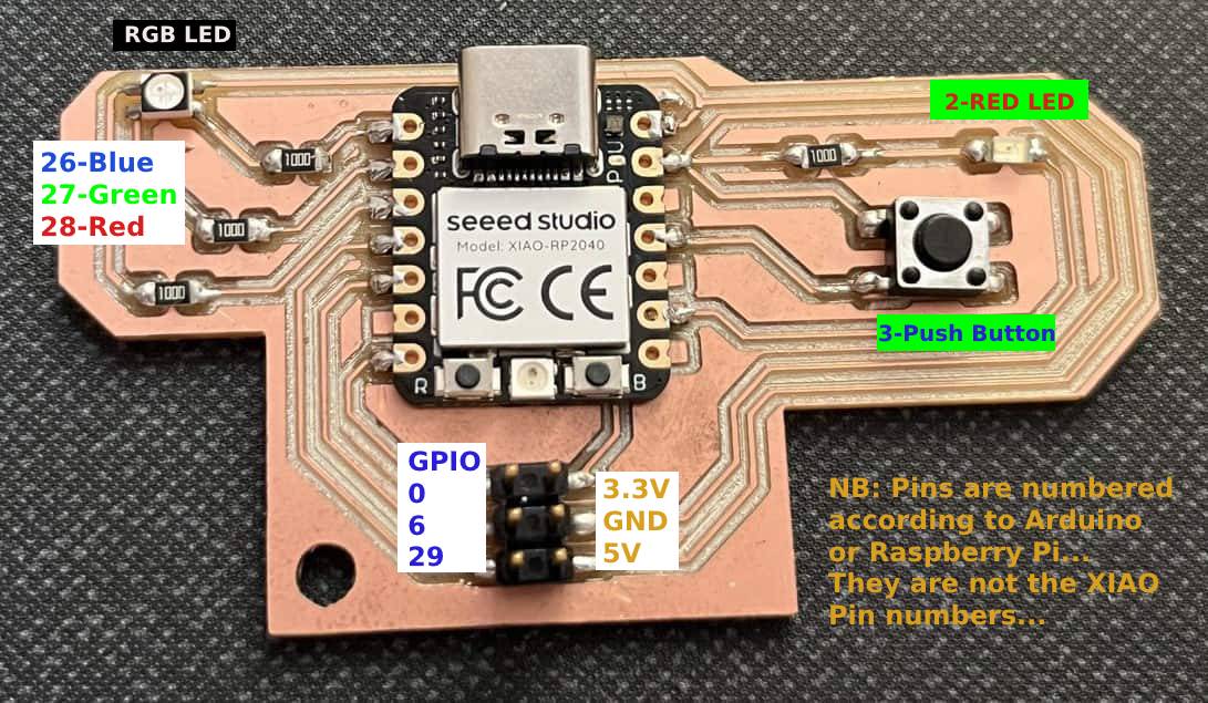
And here is the board Pin-OUT:
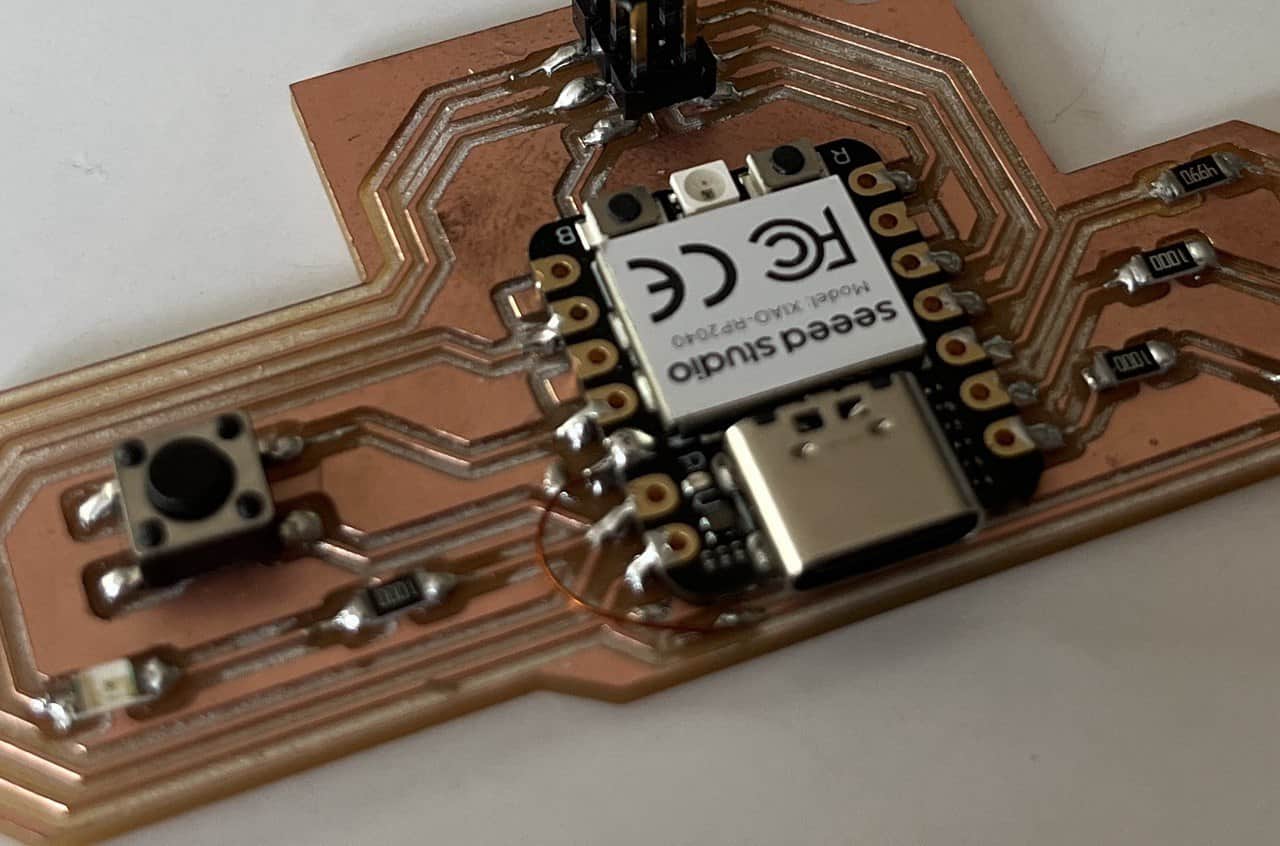
Testing the Board:
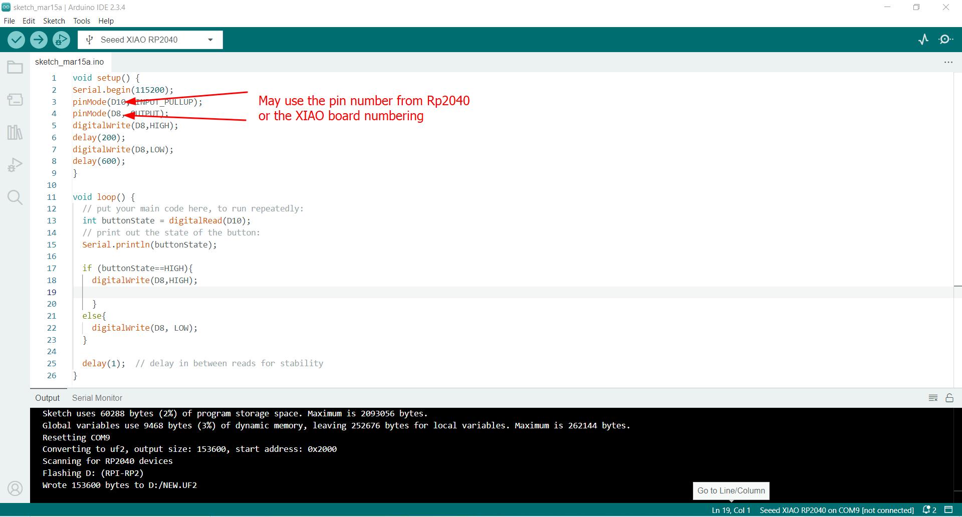
Very exciting to make the board, so first thing to do is to test it! Unfortunately the button on the board did not immediately work, but after examining the pin-out schematic, understood that the pins numbered from the RP-2040 are not in sequential order, and I had mislabeled a pin number. Here is the simple program to test the push button.
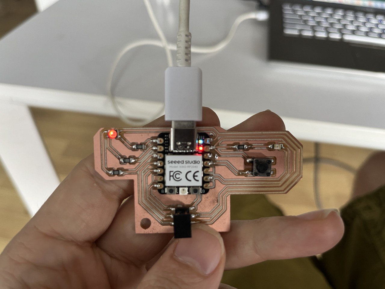
And here is a short video in action:
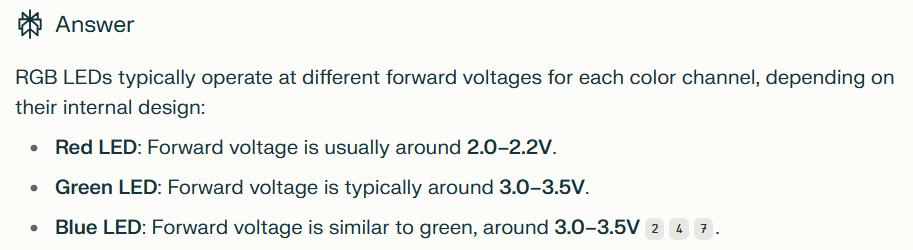
But there is a problem, of course. That is when we turn off all the LEDs the Red one still shines, but not so brightly.
This is because we connect to the 5V and the forward voltage for Red is less, only 2V.
First I tried to changed the resistor controlling the Red. Saheen suggested I desolder a resistor from an old board, so that's exactly what I did. Then I placed the higher level resistor and it mainly worked, but not completely as the Red LED still had some light even when it was turned off.
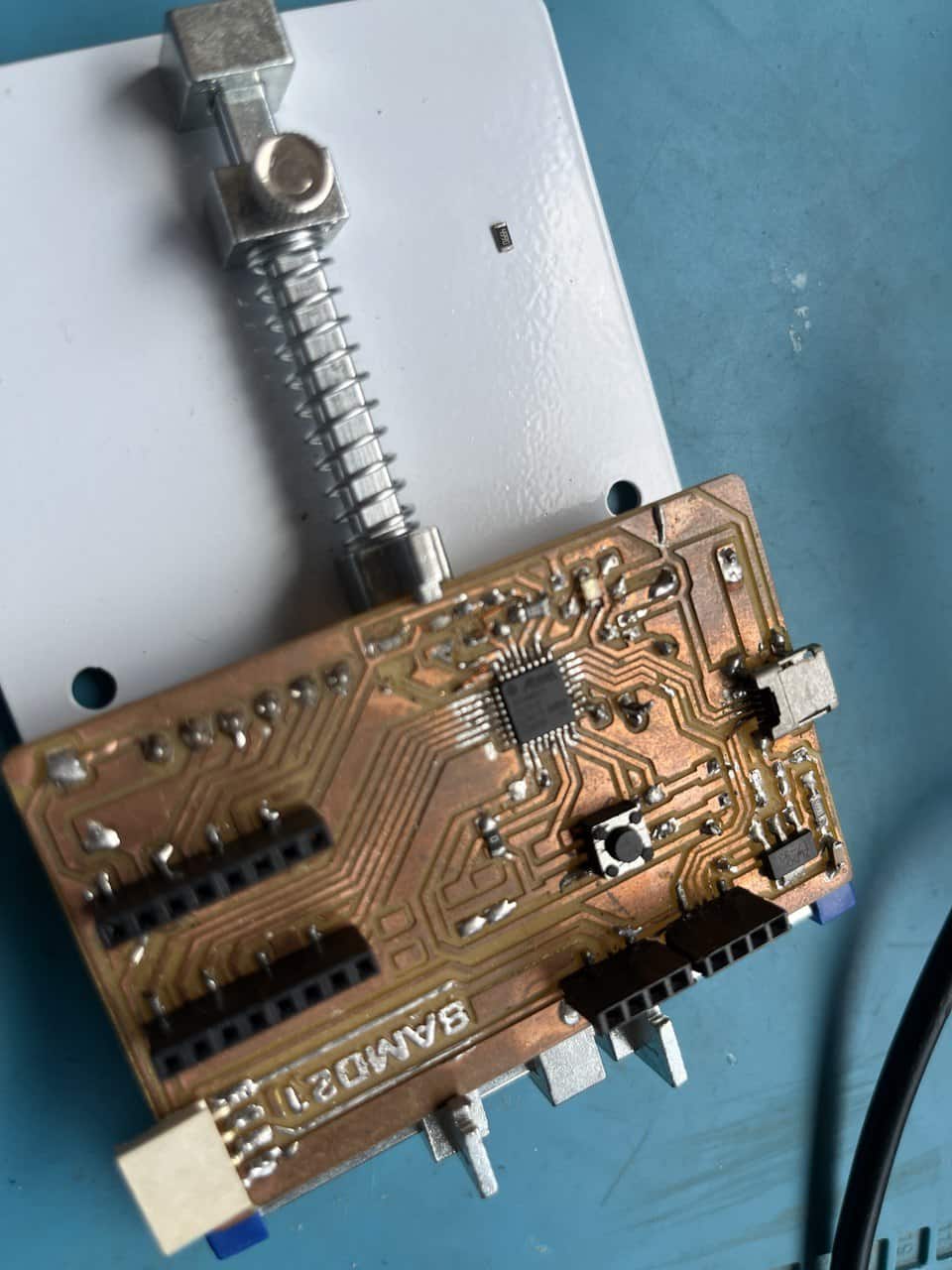
Saheen instructed how I may modify the board to connect to the 3.3V with an additional wire as can be seen below. As I recall we used the multimeter in this process to test the continuity of the new connection.
So the board is ready for continued experimentation and testing, with the lesson learned that it makes a difference whether a component is connected to the 3.3V or 5V!
Finally I made a program in both Python and Arduino that will cycle through the colours on the RGB LED. Video and program follow; you may also download files here.
int red=28;
int green=27;
int blue=26;
bool lastButtonState = 1;
int currentMode=0;
void setup(){
Serial.begin(115200);
pinMode(3, INPUT_PULLUP);
pinMode(red, OUTPUT);
pinMode(green, OUTPUT);
pinMode(blue, OUTPUT);
turnOffAllLEDs();
}
void loop(){
int buttonState = digitalRead(3);
if (buttonState == 0 && lastButtonState == 1) {
// Button was pressed, change mode
currentMode++;
if (currentMode>3){
currentMode=0;
}
updateLEDs(currentMode);
}
lastButtonState = buttonState;
delay(20);
}
void updateLEDs(int mode) {
switch (mode) {
case 0: turnOffAllLEDs(); break; // All LEDs off
case 1: turnOnBlue(); break; // Blue on
case 2: turnOnRed(); break; // Red on
case 3: turnOnGreen(); break; // Green on
}
}
void turnOffAllLEDs() {
digitalWrite(red, HIGH);
digitalWrite(green, HIGH);
digitalWrite(blue, HIGH);
}
void turnOnBlue() {
turnOffAllLEDs();
digitalWrite(blue, LOW);
}
void turnOnRed() {
turnOffAllLEDs();
digitalWrite(red, LOW);
}
void turnOnGreen() {
turnOffAllLEDs();
digitalWrite(green, LOW);
}
Hero Shot
Note that the beautiful black case shown here was designed by myself and documented in week 6.
Other PCB-making machines - X-TOOL!
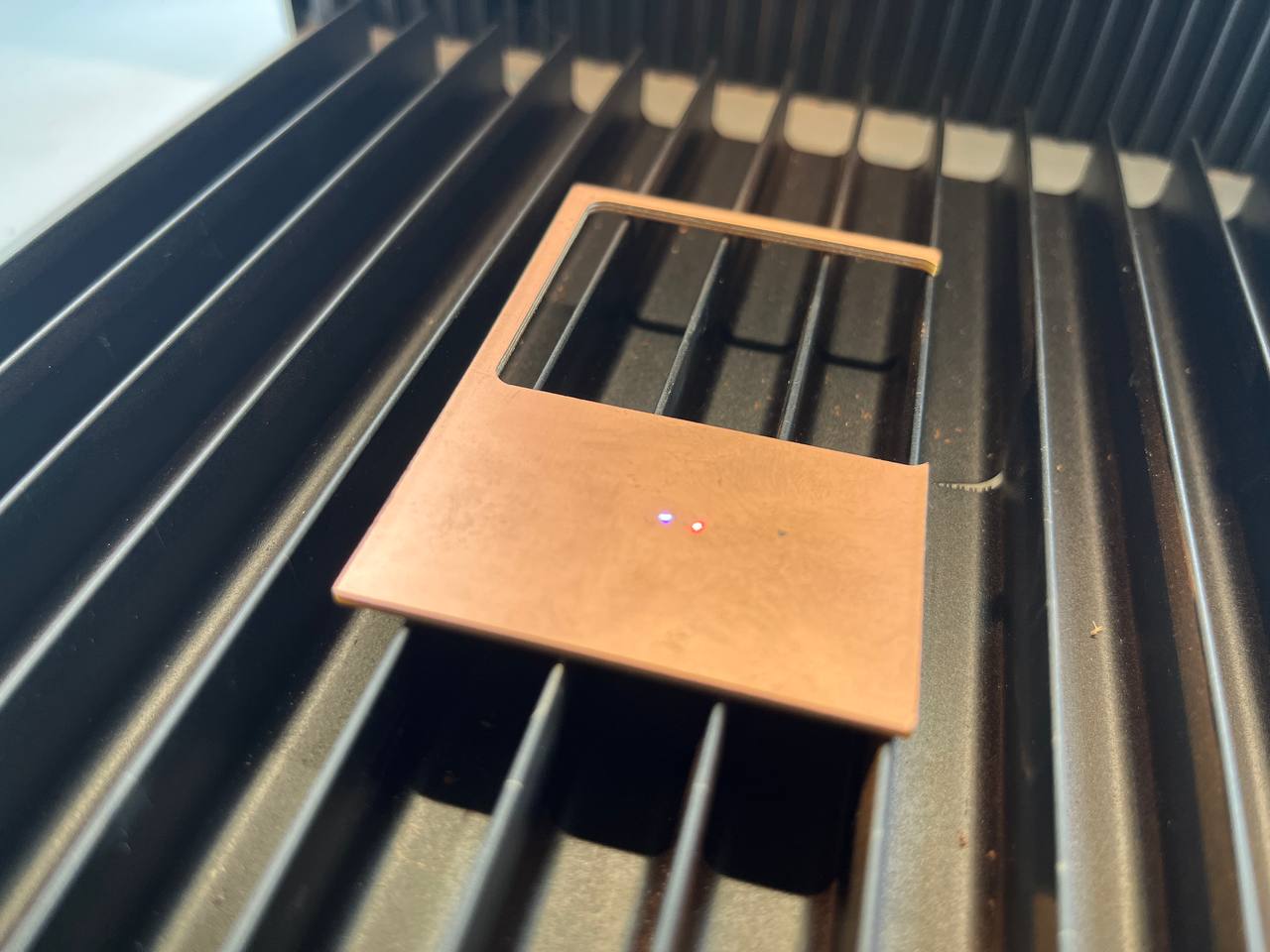
There's a new machine in lab called xTool F1 which can make the PCBs with remarkable precision using a laser. Trying to be a good boy to be allowed it. More details on their website.
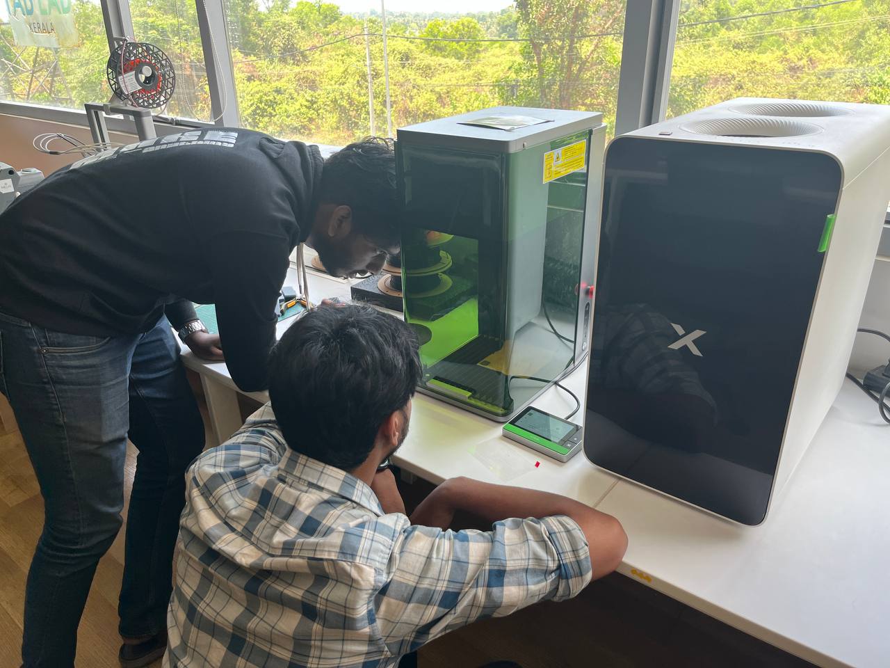
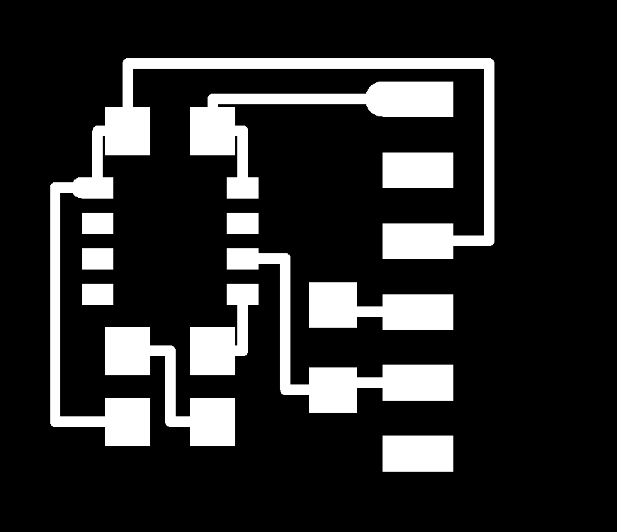
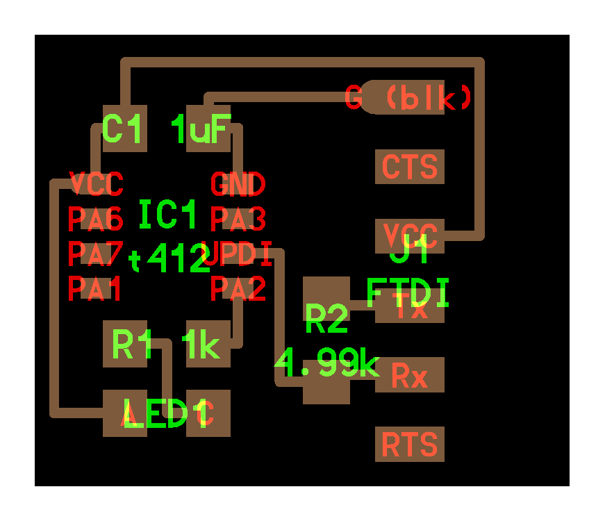
Finally this week we have a chance to use it... we will make another small board using ATTINY412, using the trace and schematic from Dr. Neil:
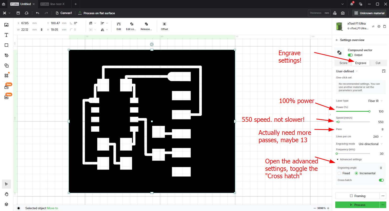
In the X-Tool software there are many settings, check them out here:
Setting up the plate in the machine, need to focus the laser:
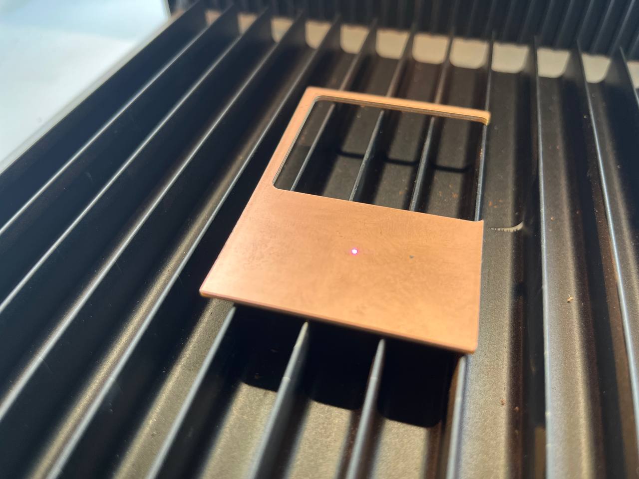
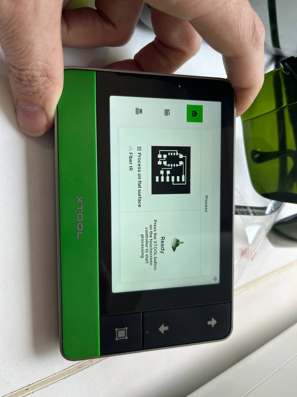
Once the laser is set and the file sent for processing, this screen should be shown on the accompanying display:
The first two times engraving were some issues. Specifically that the engraving was not complete, so settings need to be changed.
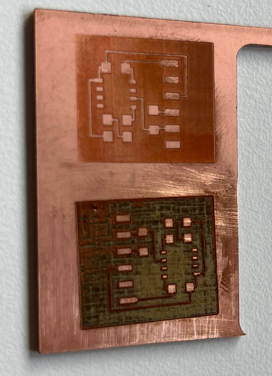
Third time is the charm? This is what the board looked like immediately after engraving completed:
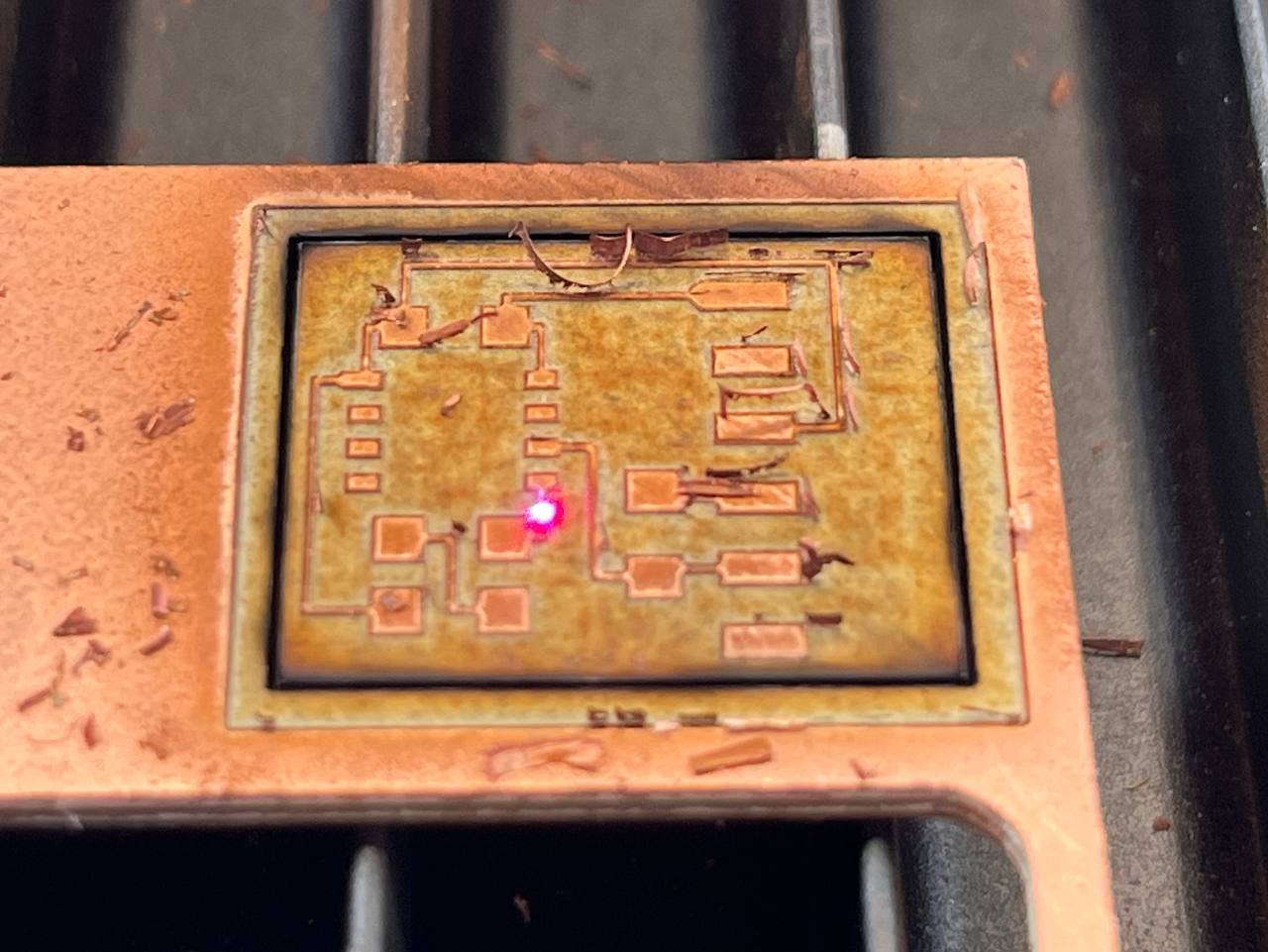
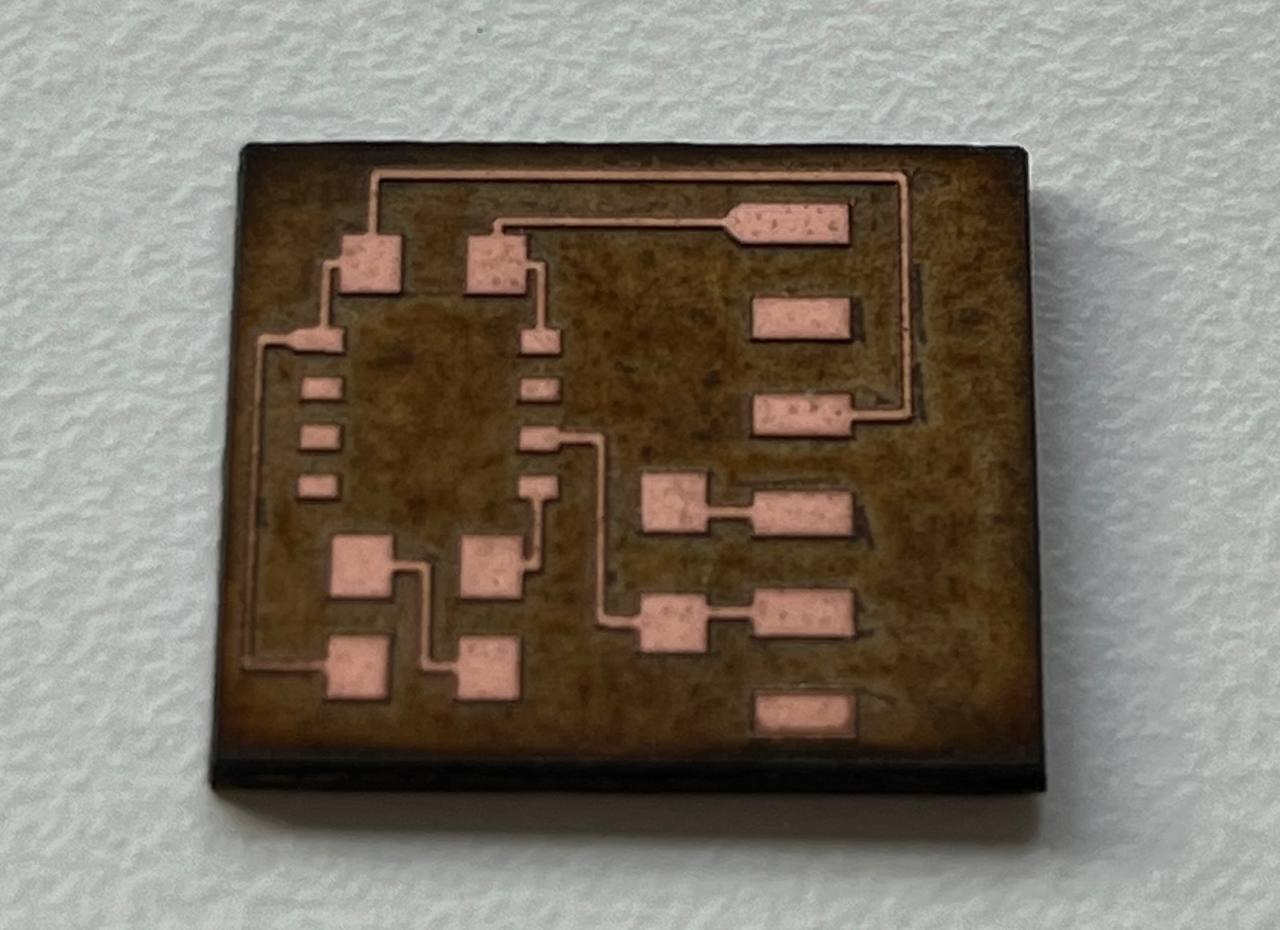
But it cleaned up very nice with the toothbrush! Now ready for soldering but it's going to be a challenge, the legs of the ATTINY are tiny!!
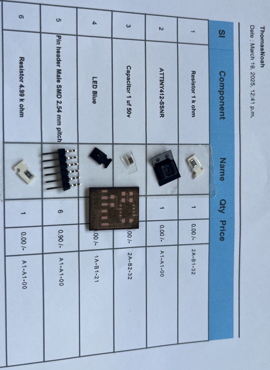
Here's the list of parts; found them all from the stash!
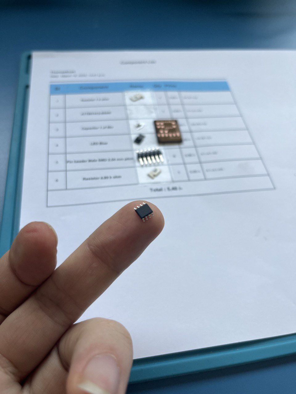
ATTiny is so tiny! But we successfully soldered in any case!
Files!
PCB - PNG filesPCB - Components
Cycle through LEDs in Python
Cycle through LEDs in Arduino