Electronics Design
Objectives for Week 6
- Use an EDA tool to design a developement board,
- That uses parts from the inventory to intract.
- Communicate with an embedded microcontroller.
- Use the test equipments in the lab to observe the operation of a microcontroller circuit board.
Individual Assignment
Group Assignment:
Group Assignment
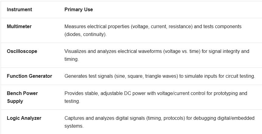
As part of our group assignment, we explored and learned how to use various electronic testing and measurement instruments. We worked with a multimeter to measure electrical properties like voltage, current, and resistance, along with testing components. An oscilloscope helped us visualize and analyze electrical waveforms, ensuring signal integrity and timing. We used a function generator to produce different test signals for circuit testing. A bench power supply provided stable, adjustable DC power for our prototypes, and a logic analyzer allowed us to capture and analyze digital signals for debugging embedded systems. Through this hands-on experience, we gained practical knowledge of these essential tools.
Group assignment link.
Basic Electronics Components
Electronic components are the elements of the circuit which help in its functioning the electrical circuit. Electronic components are the basic building blocks of an electronic circuit any electronic system or any electronic device. They can control the flow of electrons in an electronic system or electronic circuit. Refer more here.
Electronics components are classified into two;
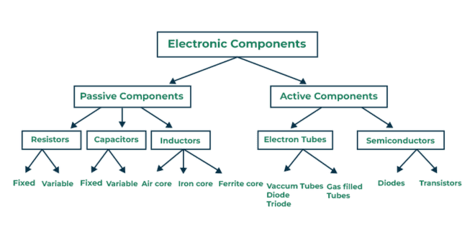
- Passive Components- Passive components are electronic devices that don’t need an external power source to operate actively. They mainly resist, store, or control the flow of electric current or voltage in a circuit.
- Resistors- Resistors control the flow of current in a circuit by offering resistance. Unit of resistance is ohm(Ω).
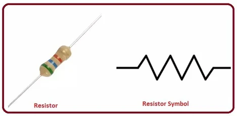
Image taken from The Engineering Projects. - Capacitors- A capacitor is a device that is used for storing electrical energy inside an electric field and using that stored energy later on for different purposes in the devices and appliances it is connected to. Unit of capacitance if farad(F).
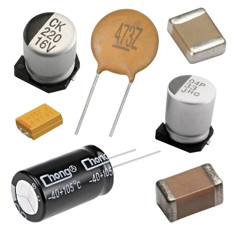
Image taken from Shady Electronics. 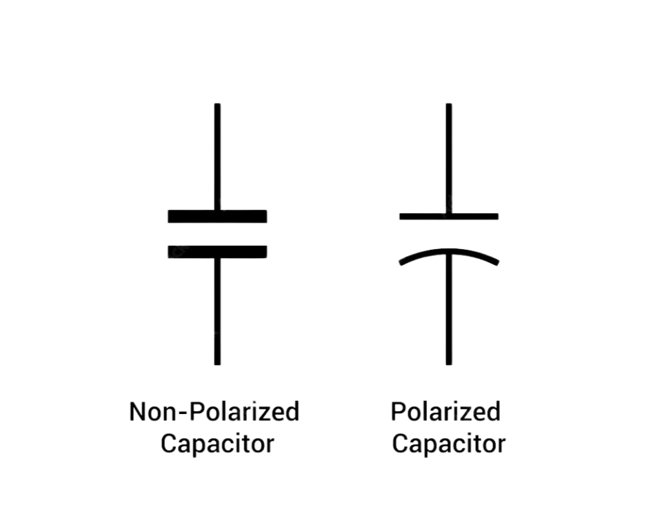
Image taken from Allelco.
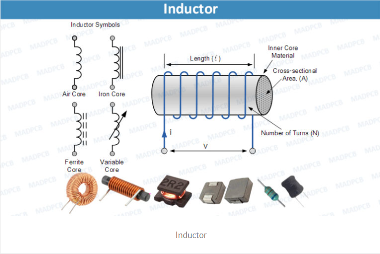
- Inductors- Inductors are electrical components that create a magnetic field when an electric current is passed through them. They store energy in the form of a magnetic field. Unit of Inductance is henry(H).
- Active Components- Active components are electronic devices that need an external power source to work. These components can amplify, switch, or generate electrical signals.
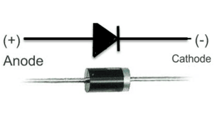
- Diodes- A diode is a semiconductor device, typically made of silicon, that essentially acts as a one-way switch for current. It allows current to flow easily in one direction but restricts current from flowing in the opposite direction.
- Transistors- Transistor is an electronic component that amplifies electrical signals. They are commonly used in amplifiers, digital logic circuits, and voltage regulators.
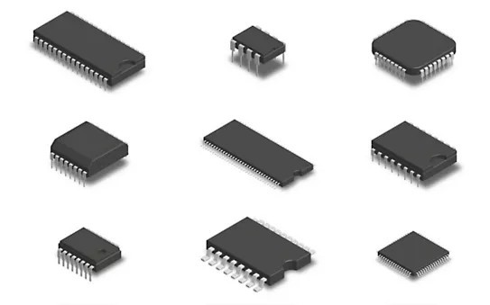
- Integrated Circuits- An integrated circuit (IC) is a small electronic chip that combines many components like transistors, capacitors, and resistors on a single semiconductor.
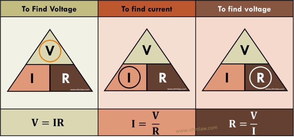
Ohm's law
Ohm's Law states that the current in a circuit is directly proportional to the voltage and inversely proportional to the resistance.
V=I x R
PCB Designing
Electronic Design Automation(EDA) Software
EDA softwares are used to design, analyze and simulate PCB layouts. These tools help us to develop and test circuits before manufacturing. Some of the EDA softwares are listed below,
- Fusion 360
- KiCAD
- Altium Designer
- OrCAD
- EasyEDA
For designing my PCB, I used KiCAD software. It is a free and Open source EDA. To download KiCAD, click here. To familarize the KiCAD, Midhun our previous year Fab Academy graduate took a session of how to use KiCAD to design a circuit.
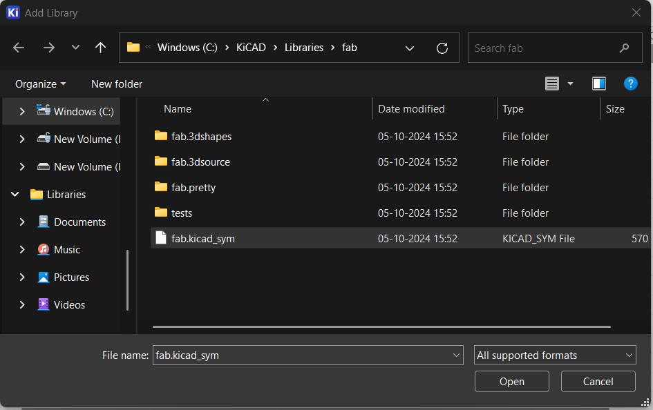
To acces the Fab Academy's library of footprints and symbols for KiCAD, I downloaded the .zip library from here.
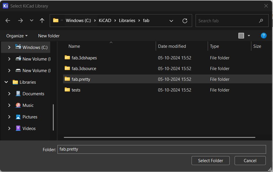
In local disk C, I created a folder named "KiCAD' and inside it I created another folder named 'Libraries' and cloned the library from Fab Academy and renamed it as 'fab'.
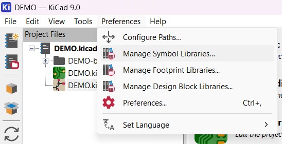
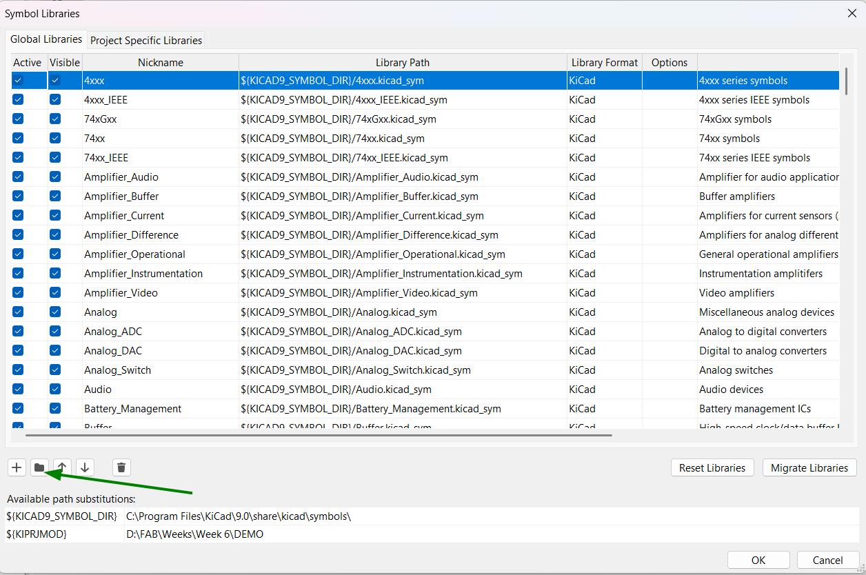
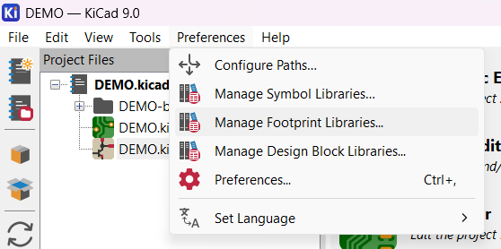
I followed these steps to add the libraries to KiCAD:
- Open KiCAD
- Preference → Manage Symbol Libraries.
- From 'Add existing library to table' and selected symbol file from the Folder I cloned earlier.
 |
 |
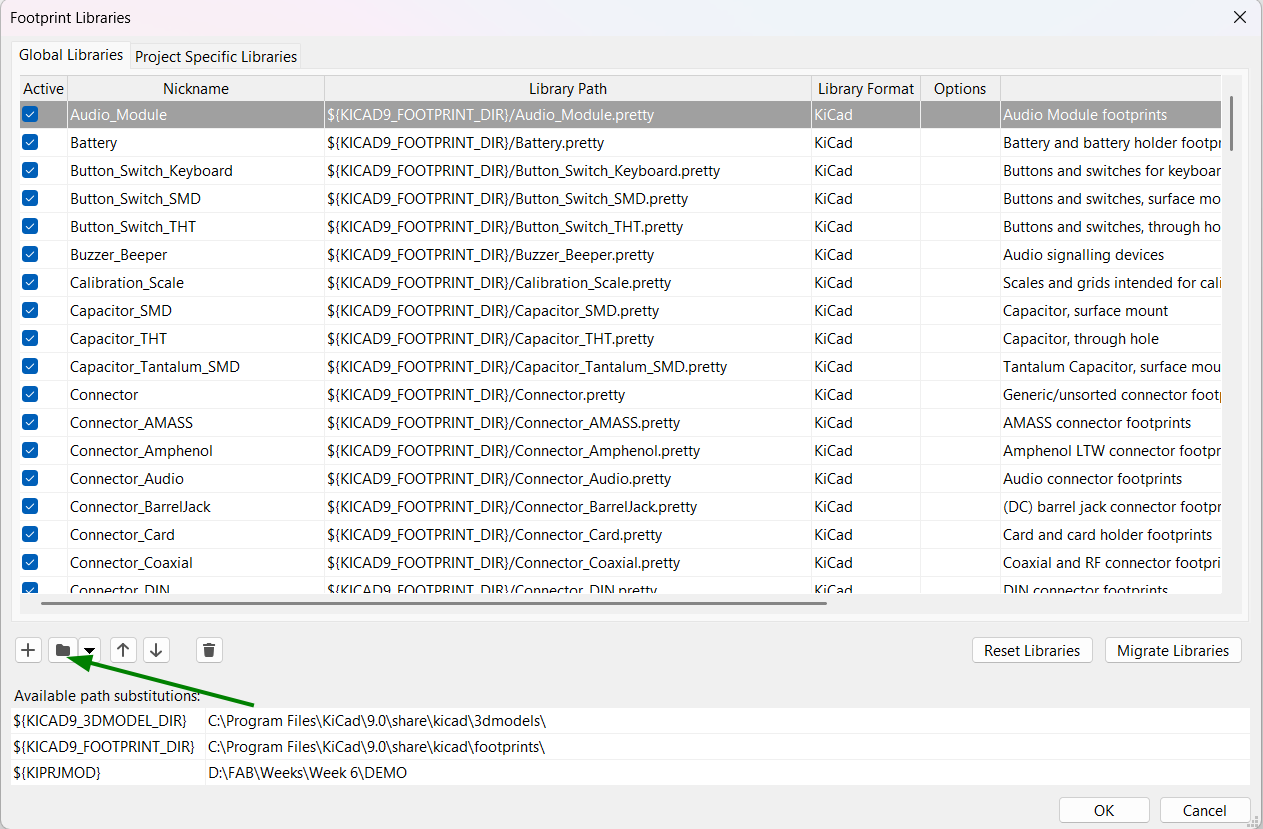
I followed these steps to add the footprint library.
- Open KiCAD
- Preference → Manage Footprint Libraries.
- From 'Add existing' I selected the footprint file.
 |
 |
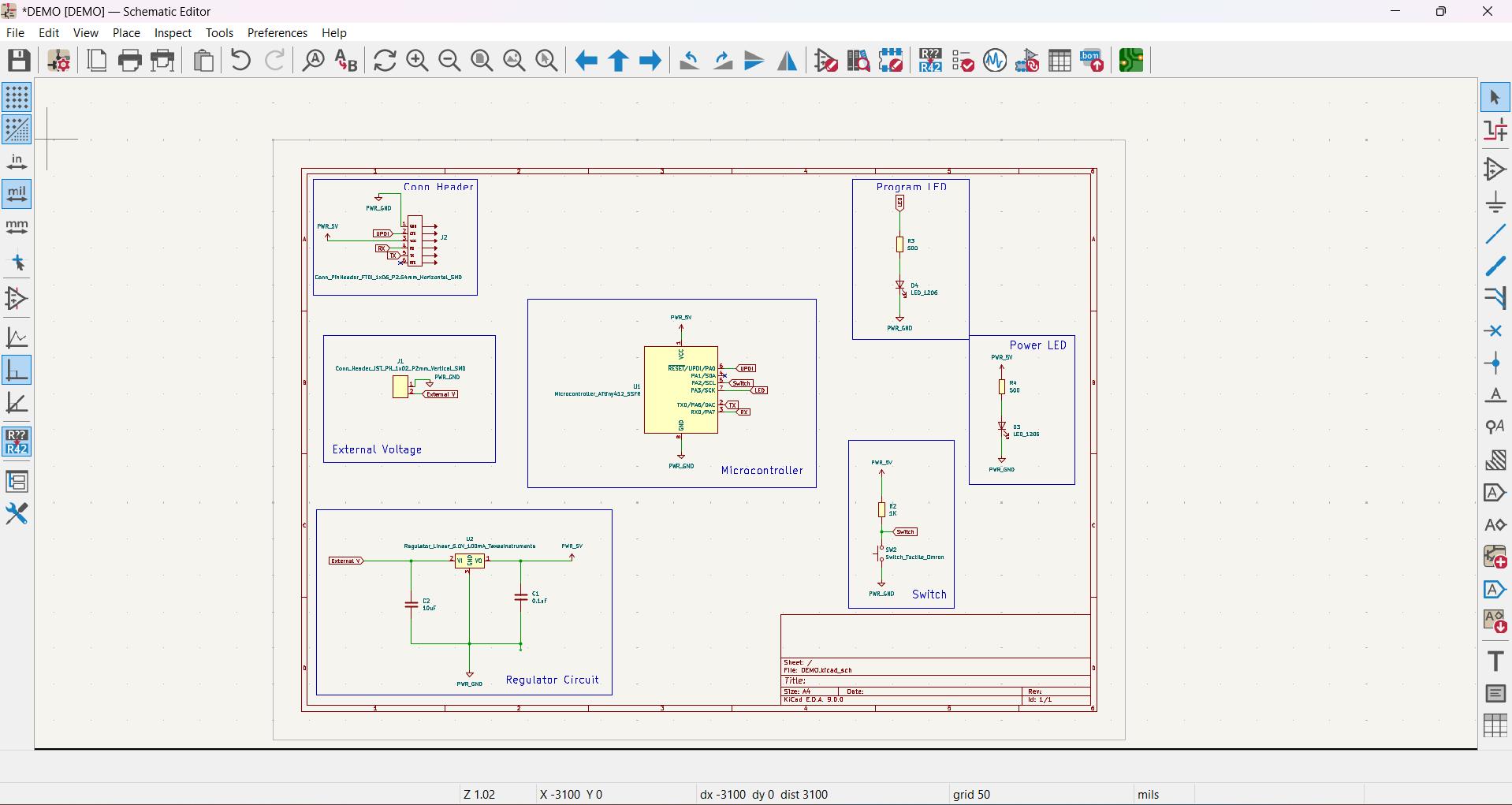
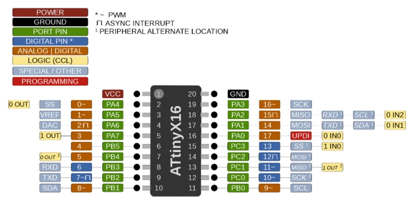
For familirising KiCAD, our instructors help us to design a PCB using ATtiny412 microcontroller. From the datasheet of ATtiny412 I identified it works on 5V. The step by step designing is listed below,
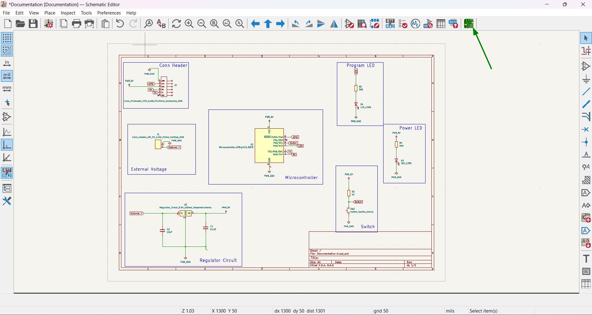
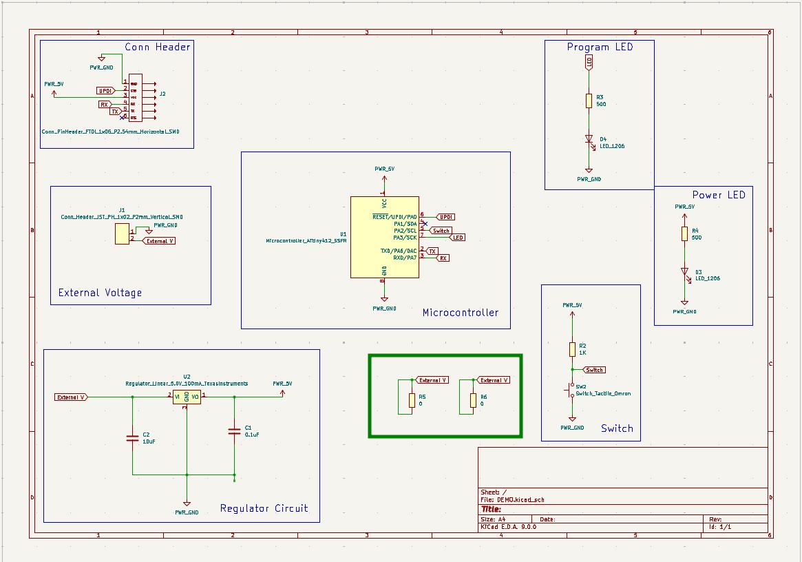
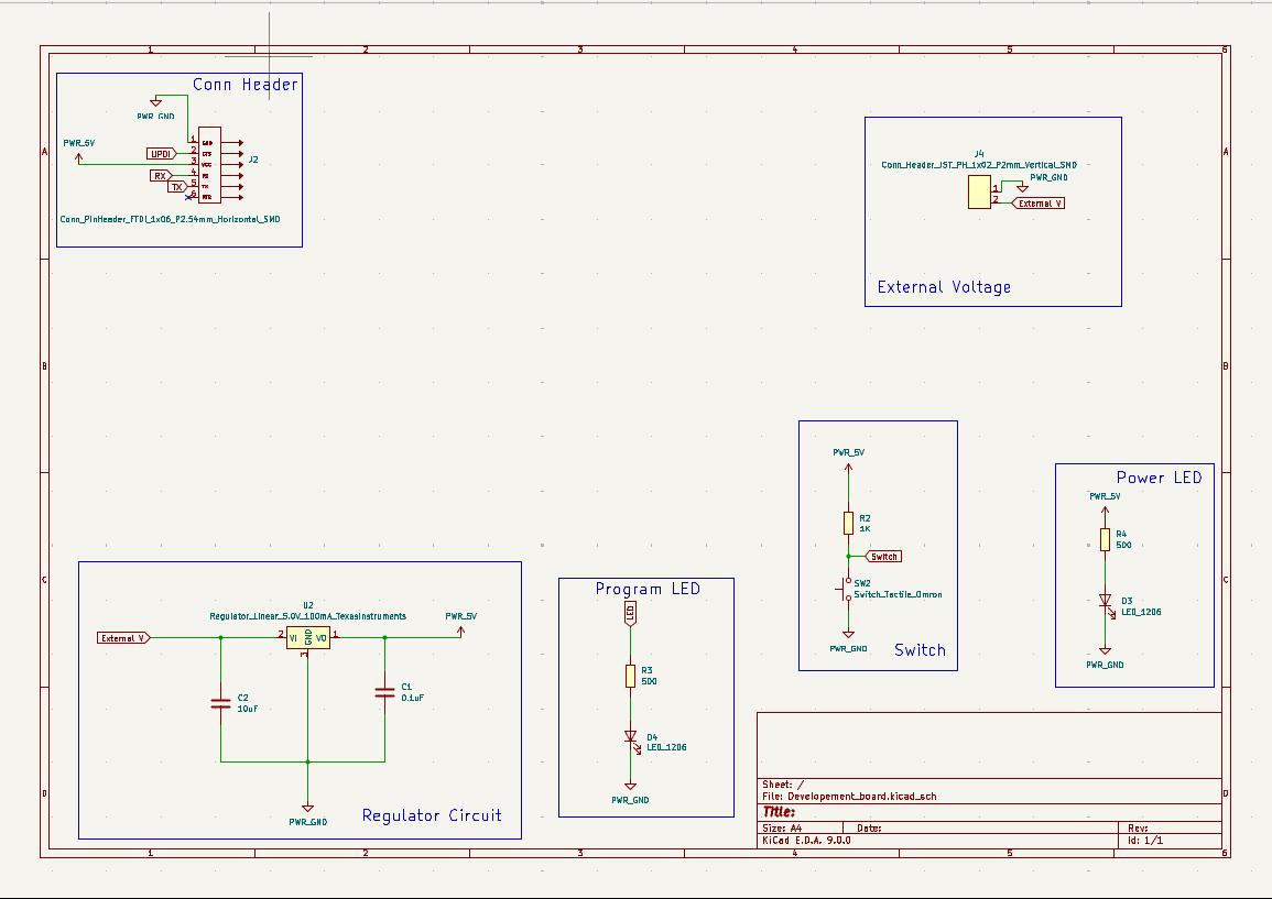
Schematic Design
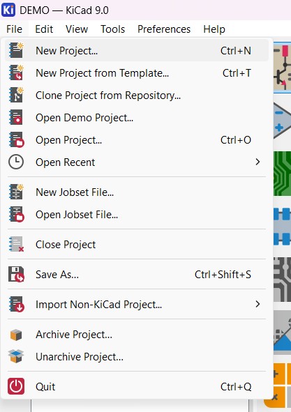
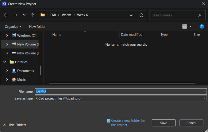
- File → New Project and save the file.
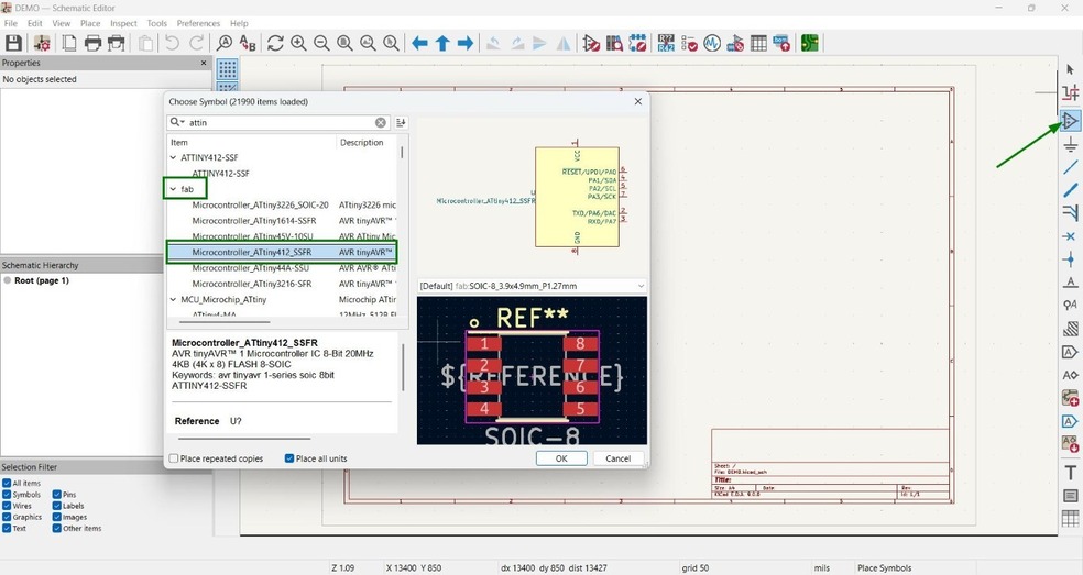
- Place Symbols → Add ATtiny412 from fab.
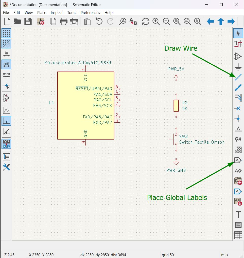
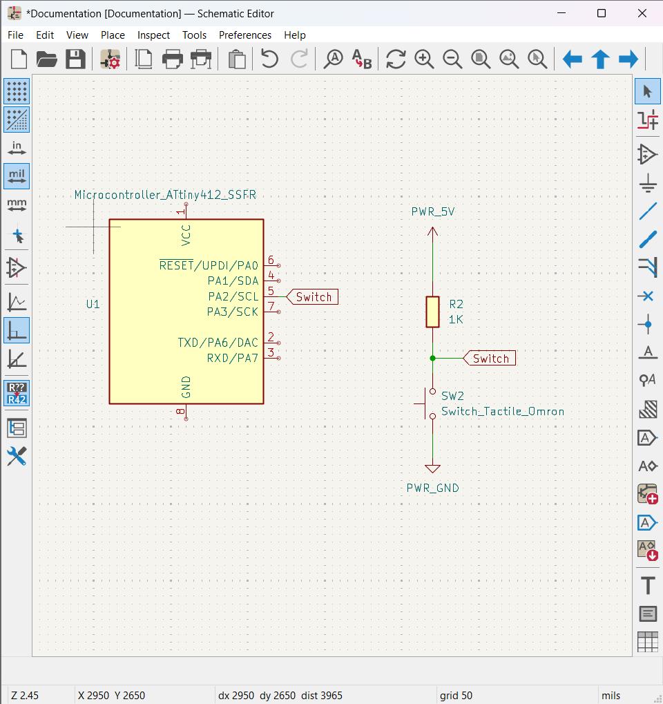
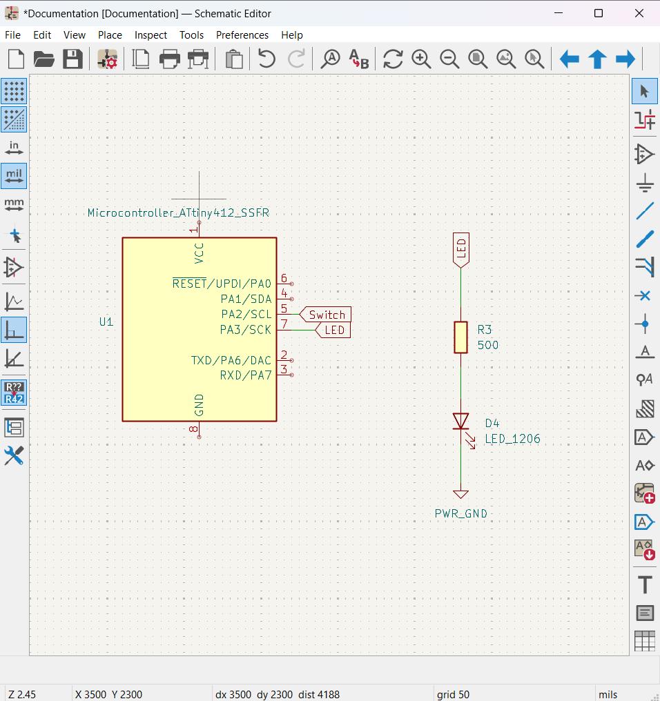
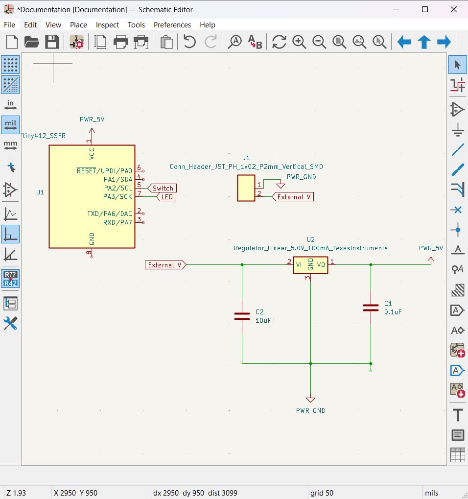
- Added Switch, 1K resistor, 5V supply and ground. Wire it using 'Draw wires' and 'Place Global Labels' connected it to SCL pin of ATtiny412.
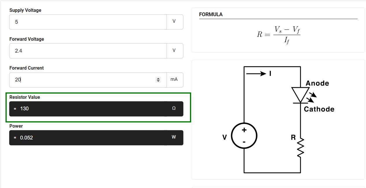
- Added LED and Resistor and connected it to SCK pin of ATtiny412. I used Red LED here. The forward voltage of red LED is 2 to2.4V and forward current was 20mA. The supply voltage was 5v. These values are obtained from the datasheet. I used Digikey website to calculate the resistance needed for the LED. The resistance value obtained is 130Ω. We only had 100Ω and 500Ω resistors in our lab and I need to choose the nearest higher value resistor and hence I chosed 500Ω resistor for LED.
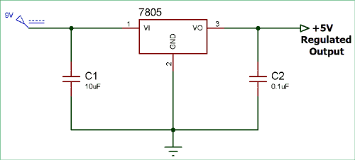
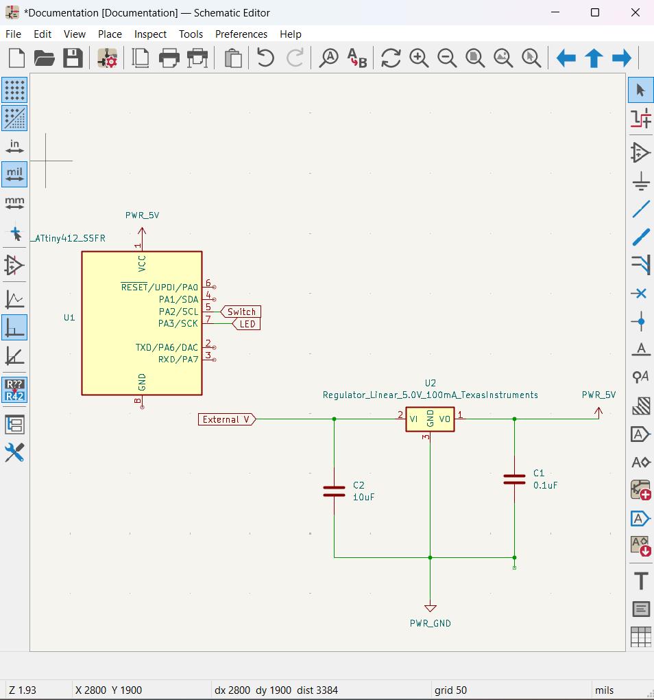
- I initially needed to design a regulator circuit, but I added it later. I referred to Google for guidance and found a suitable regulator circuit.
- For powering the circuit, I added external voltage source.
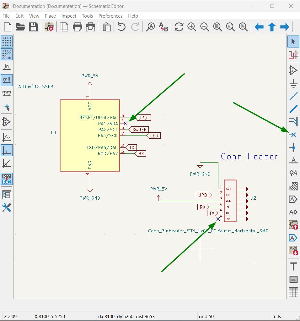
- For programming the microcontroller I added 6 Pin Conn Header pins. Using 'Place Global Labels' I added the connections. Using 'Place No Connect Flags' I crossed the pins which are not used in this circuit.
- I arranged the circuits for identifying it easily.
 |
 |
 |
 |
 |
 |
|
 |
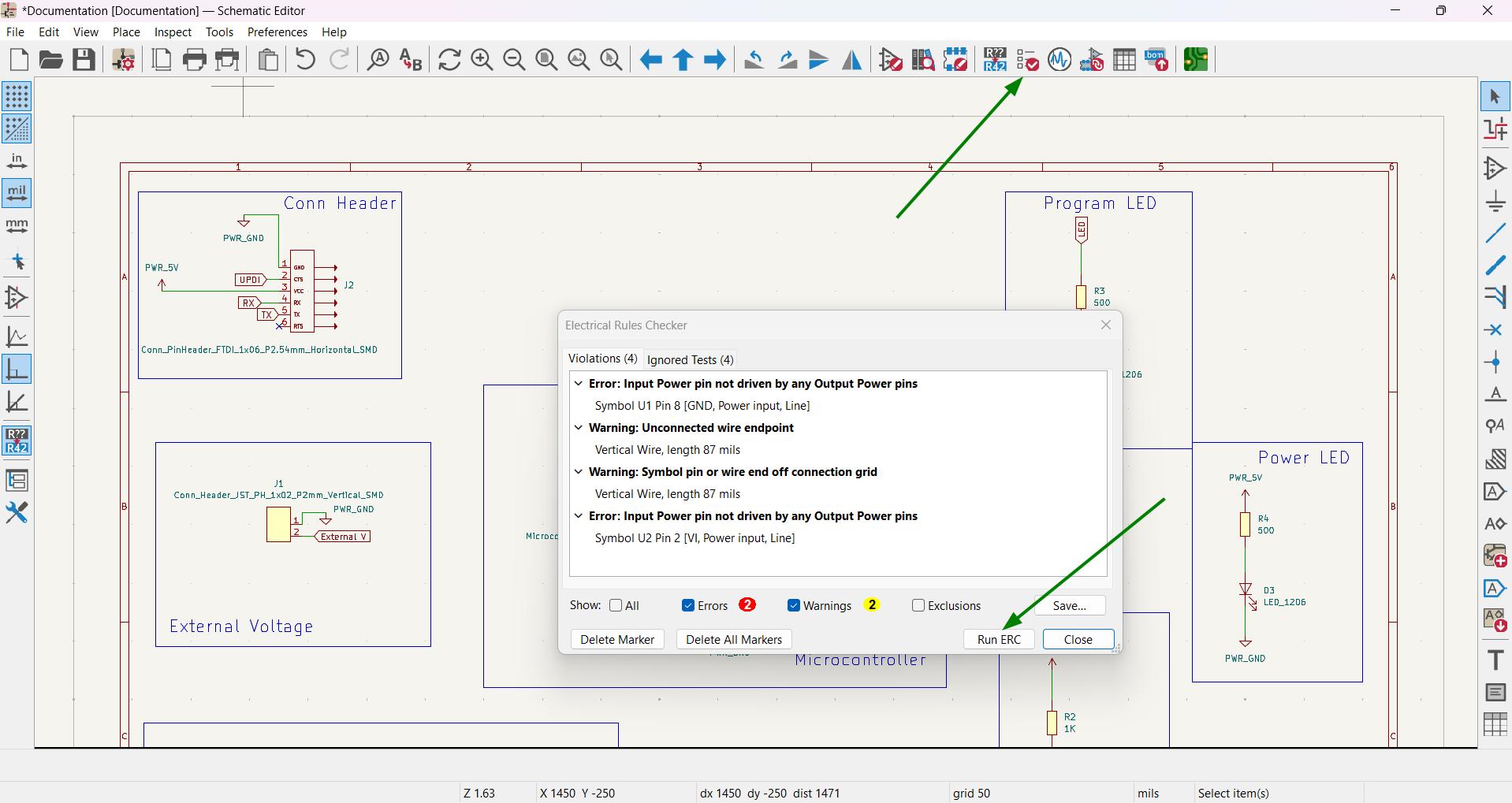
Electrical rules checker (ERC)
In KiCad, ERC stands for Electrical Rules Check. It is a tool used to check if the schematic is logically correct. ERC helps identify issues like unconnected pins, incorrect connections, or missing power sources. Running ERC ensures that the circuit will work as expected before moving on to the PCB design. While running ERC I got 2 errors and our instructors told that those errors can be skipped.
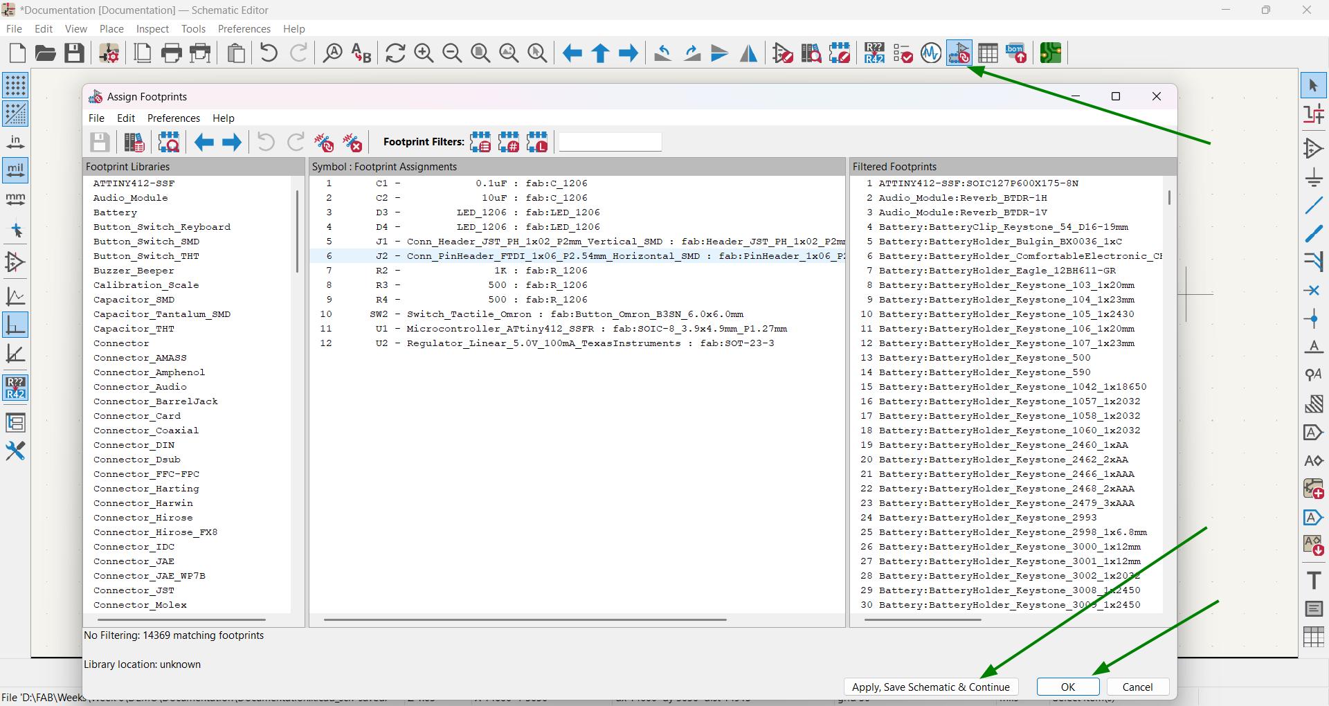
Footprint
A footprint is the physical layout of a component on the PCB. It shows where the pins, pads, and outline of the component will be placed on the board. While the schematic symbol shows how a part connects in the circuit, the footprint makes sure it fits correctly on the PCB for soldering and assembly. I used the footprints from the fab footprint library.
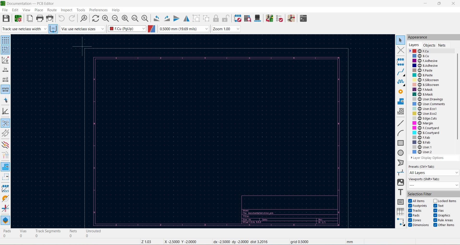
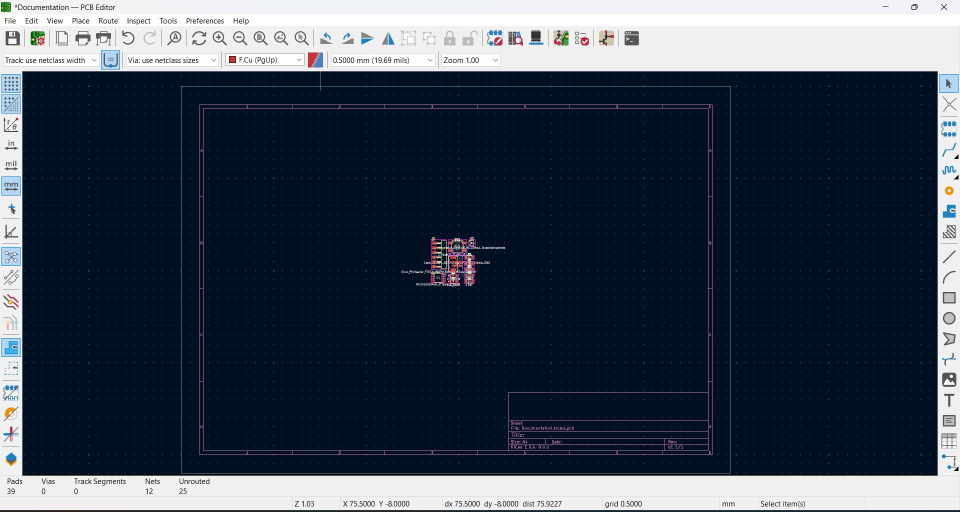
PCB Editor
In PCB editor we can design the actual circuit board. After designing the circuit in the schematic editor, I used the PCB editor to place the components and draw copper tracks that connects them. We can directly switch from Schematics editor to PCB editor.
 |
 |
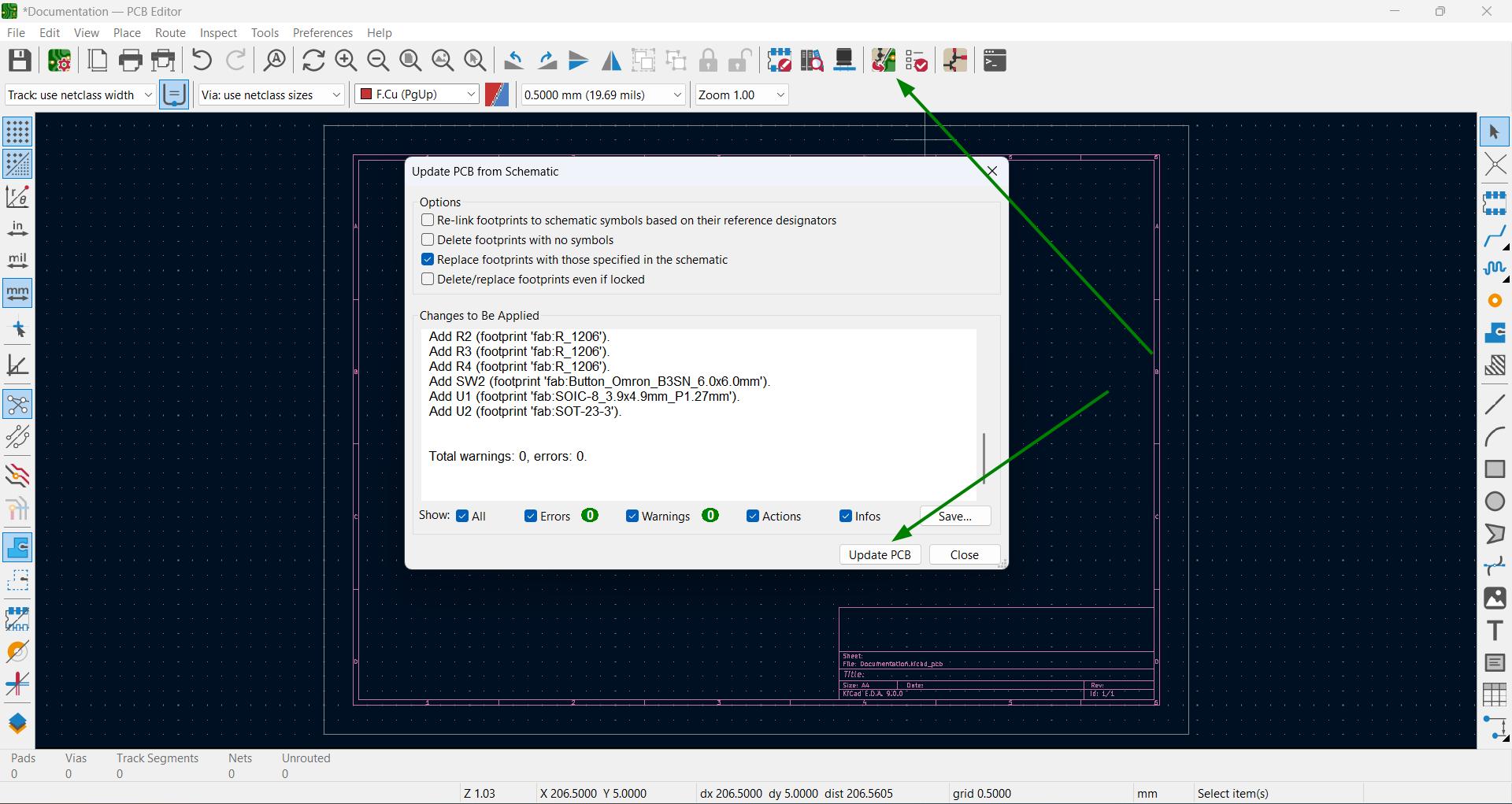
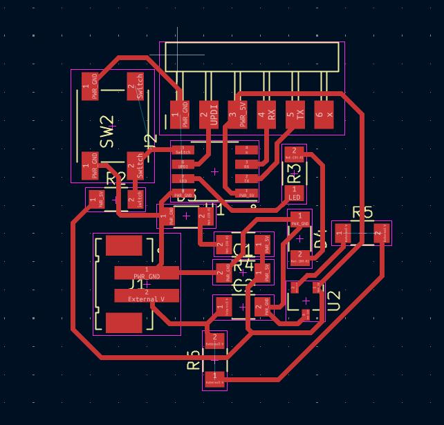
- Using Update PCB from schematics option the Schematics we designed was loaded as footprints in the PCB Editor.
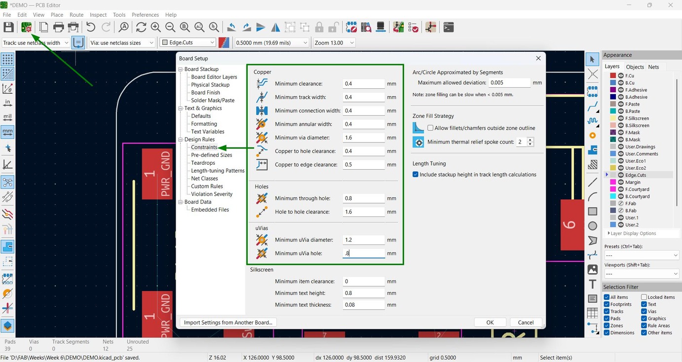
- In Board Setup add constrains. These constrain values are based on the PCB milling machine and Tool available in our lab. The constarins were taken from Rayan's documentation.
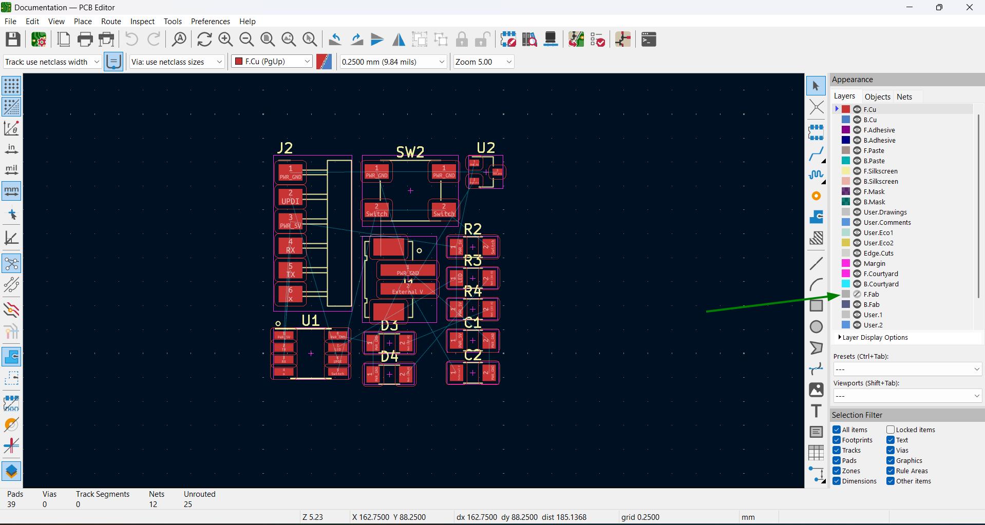
- Hide the F.Fab layer to hide the naming of the footprints.
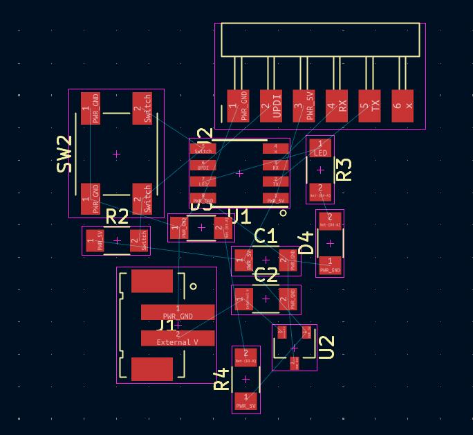
- Rearranged the footprints by observing the air wire inorder to route it easily.
- Using Route single track option I routed the wires. Always ensure that The layer is in F.Cu while routing. While routing ensure that the power and ground should be routed lastly. After routing 2 pads can't be connected directly. So I used 0 ohm resistor to connect these pads toughter. Still there are some air wires shown in the PCB editor. As they were internally connected it was not essential to connect them. That's why it was kept unrouted.
 |
 |
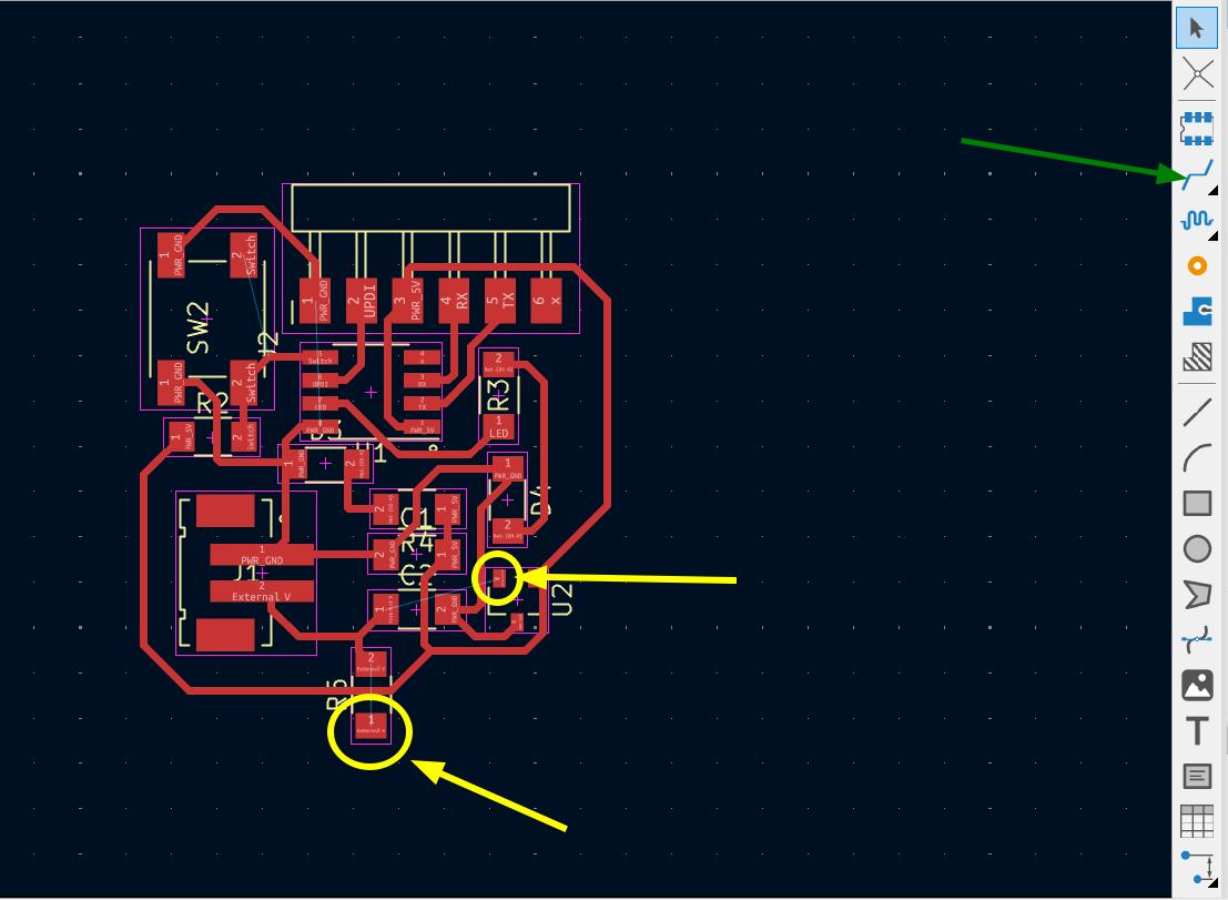 |
 |
Outline
Then I draw a renctangle edge cut. Ensure that the layer is in Edge cut while adding edge cut.
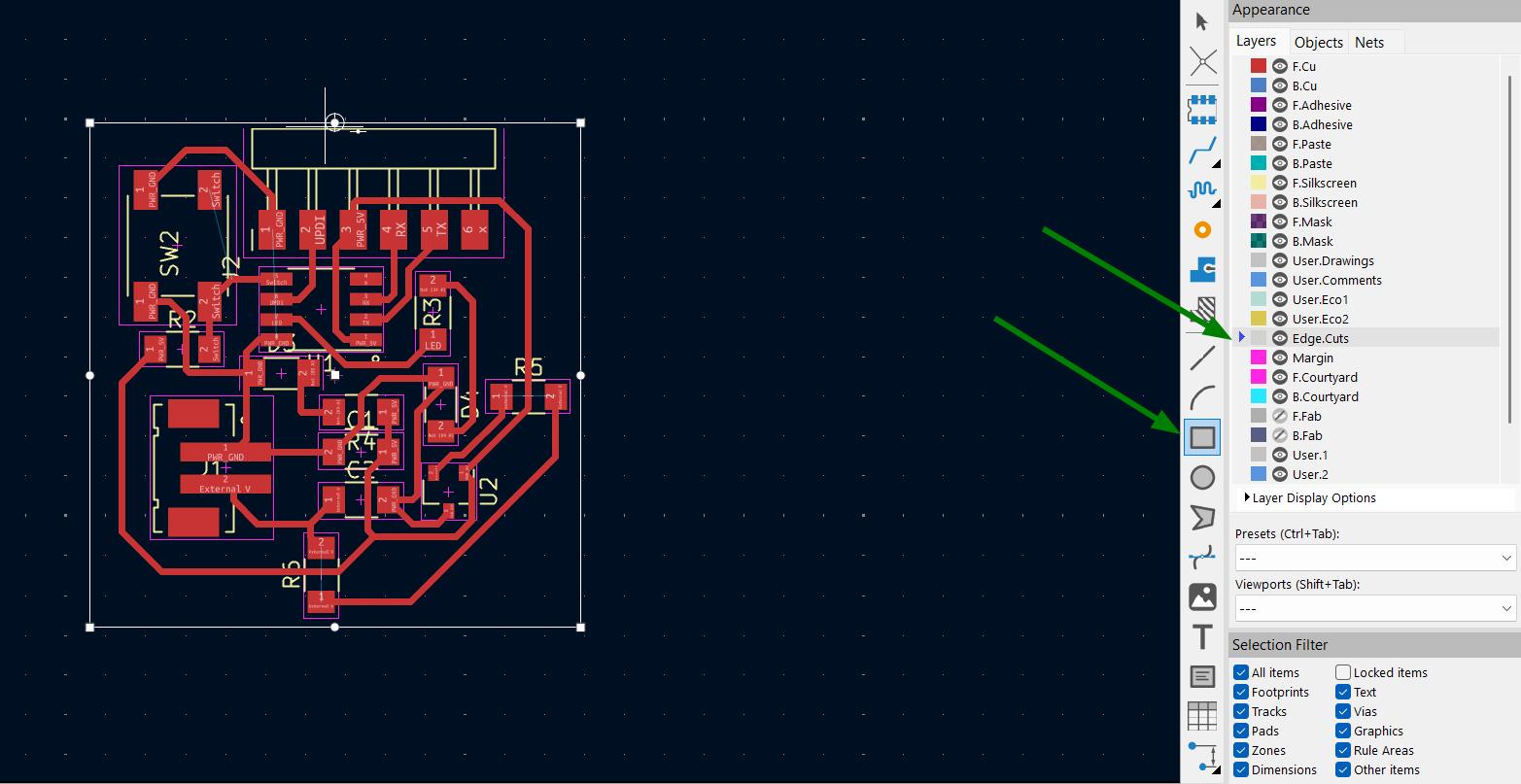
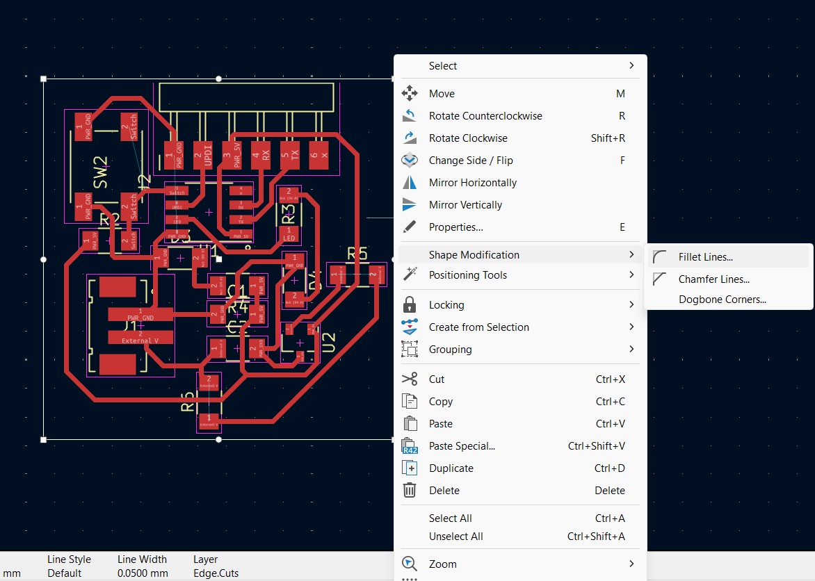
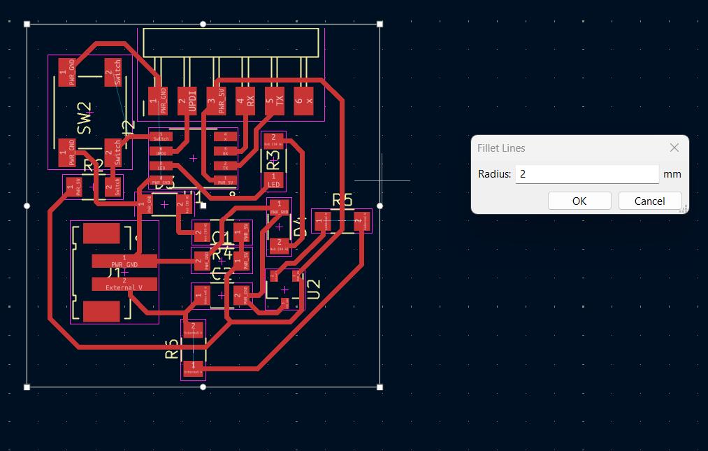
I added fillet to avoid the sharp corners. For that Right click on rectangle → Shape Modification → Filet lines and add the radius.
 |
 |
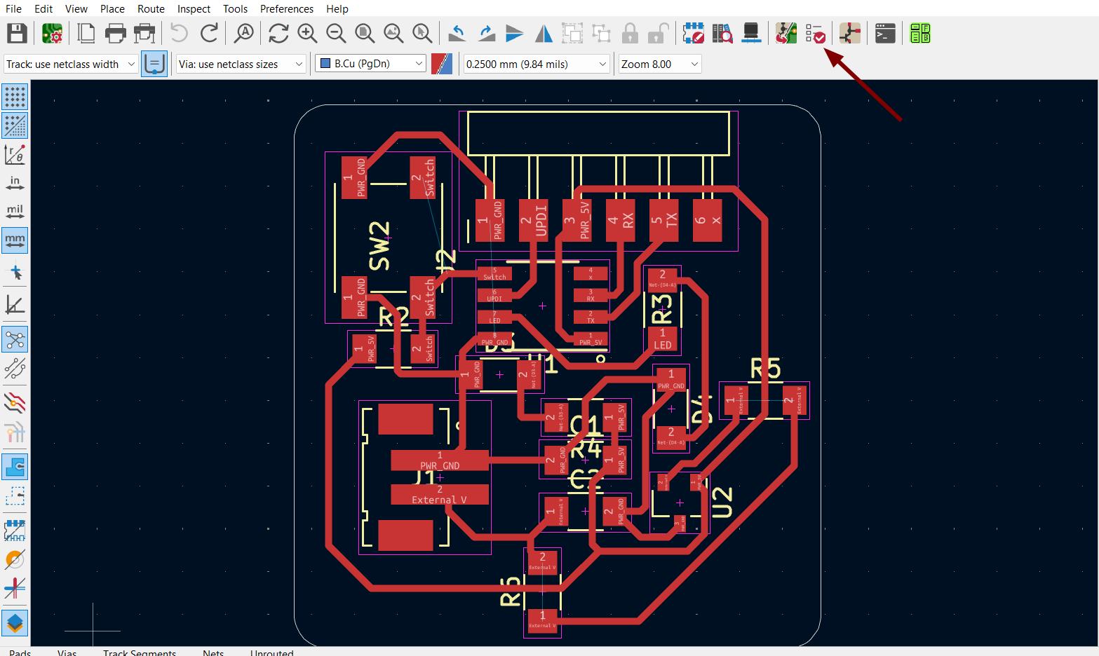
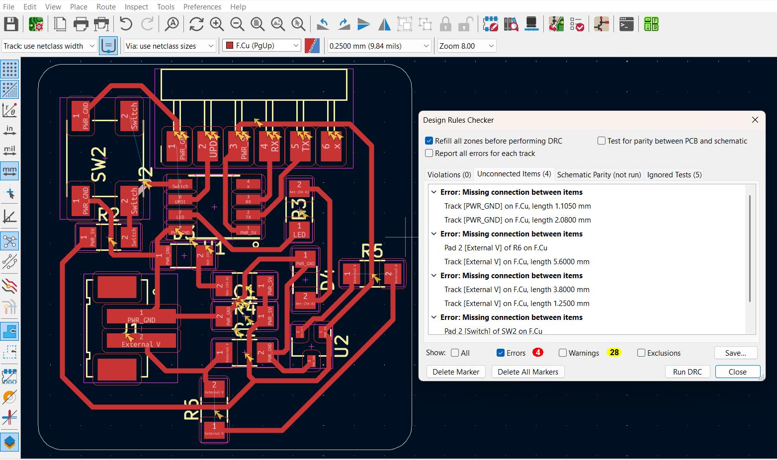
Design Rule Checker (DRC)
DRC checks the PCB design to make sure everything is placed and connected properly. It helps find mistakes like tracks that are too close or parts that are overlapping, so thr board works well and can be made without issues.
I ran the DRC and got some errors. The errors were mentioning some missing connections and as they were inernally connected it was not essential to connect those mentioned errors. So those errors can be neglected.
 |
 |
Individual Assignment
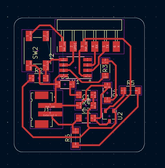
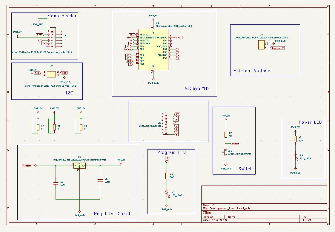
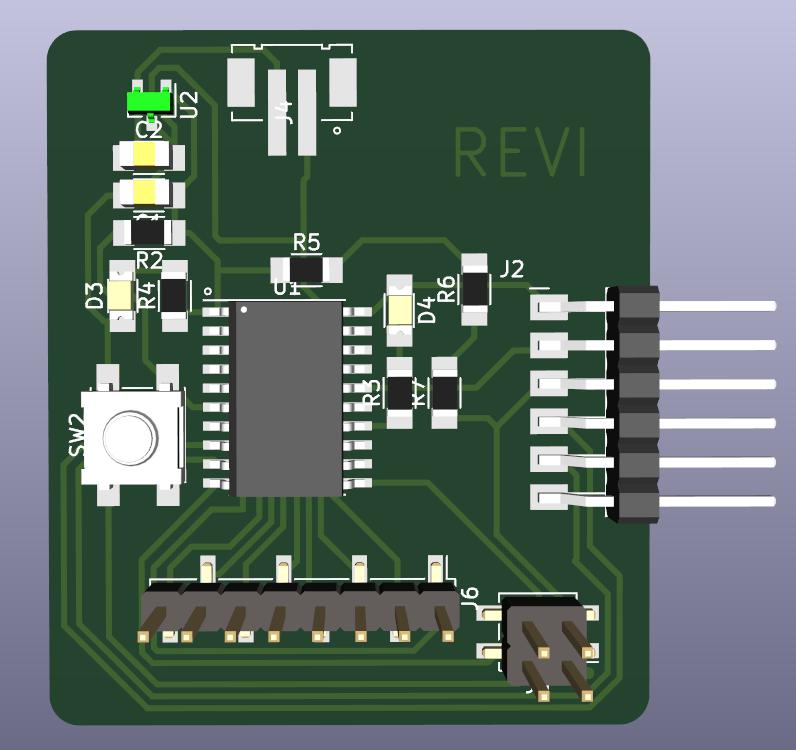
For this week's assignmnet I need to create a develpement board using any one of the micro controller available in the lab and which is related to my final project. I need to play audio from SD card and tilt the head of the toy at a particular angle as well in my project. So after discussing it with my instructors I chosed ATtiny 3216 microcontroller to design my developement board. After refering the datasheet, I conformed it need 5v to work. So I can use the similar Schematics and components from the board I designed earlier.
I created an New Project and saved it. The schematics was similar to the one I designed earlier and I just copy and pasted the circuits which I needed in the new design.
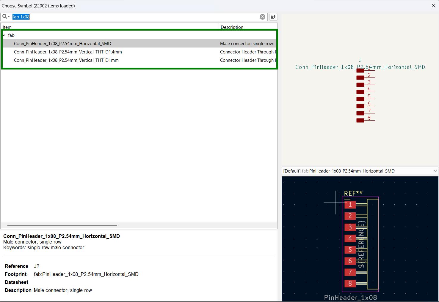
The 1x08 header pin Symbol and Footprint was not available in the fab library. So I added it from KiCAD library.
 |
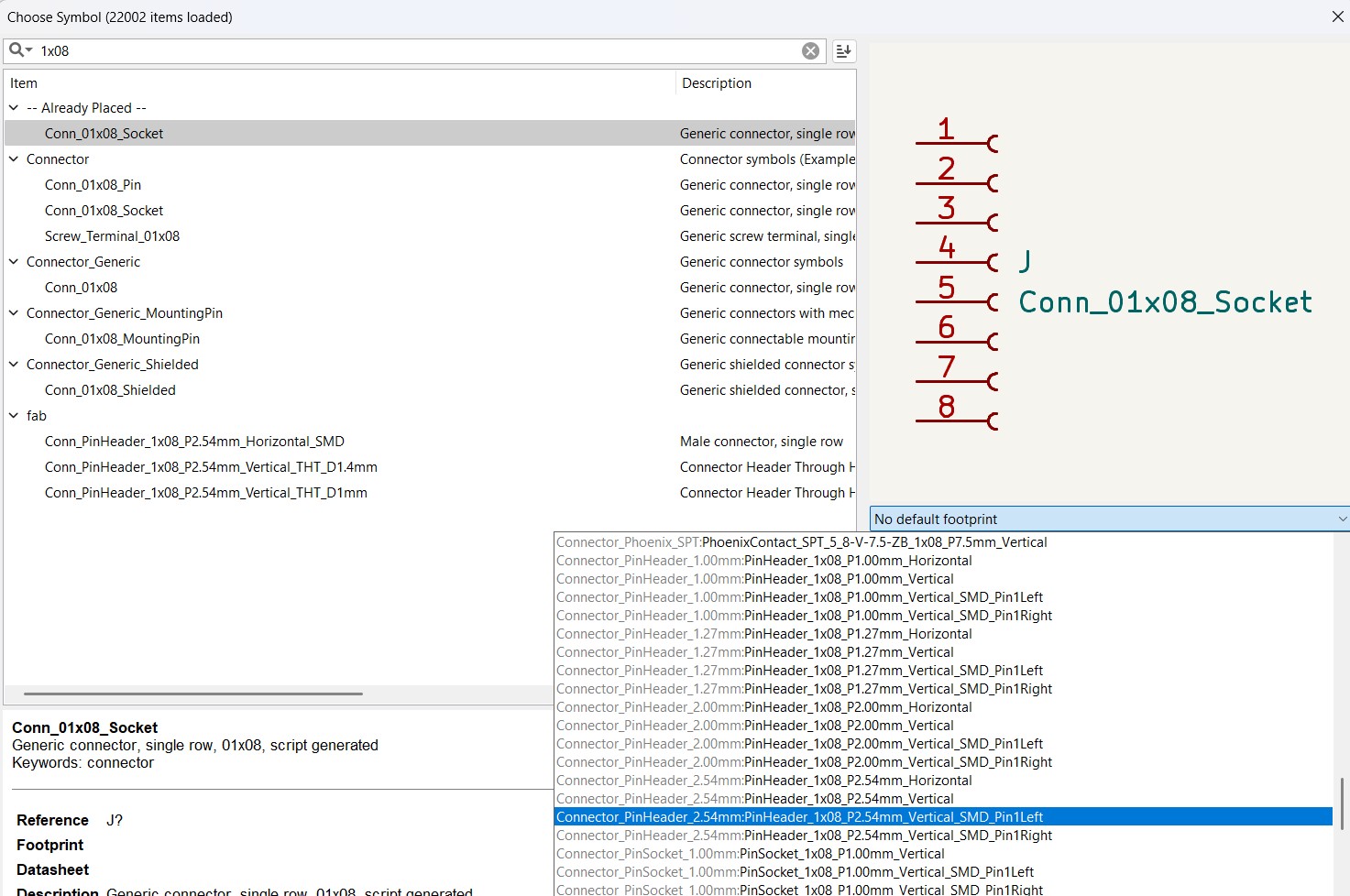 |
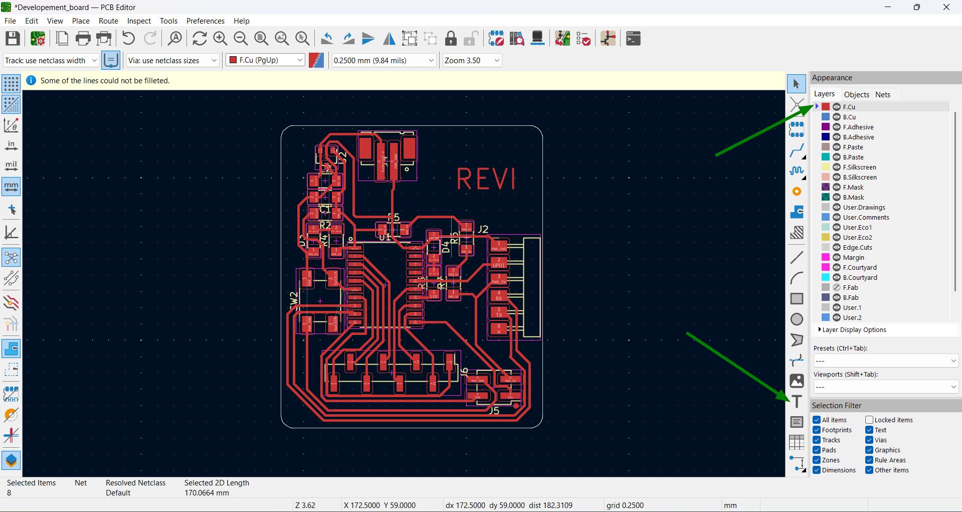
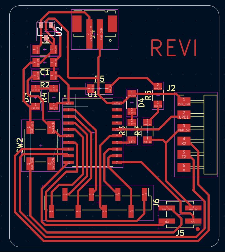
Added ATtiny 3216 microcontroller, Conn_PinHeader_2x02 for I2C connection and Conn_01x08 header pins for taking out all other pins of micro controller. While routing it in PCB editor I needed to add 3 0 ohm resisitor to provide power for I2C devices. I added my name in the PCB for that I changed it into F.Cu layer and Using Draw Text option I added my name.
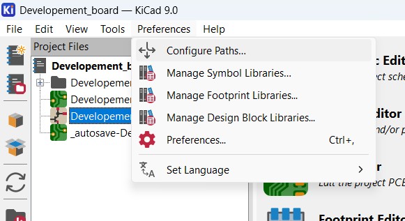
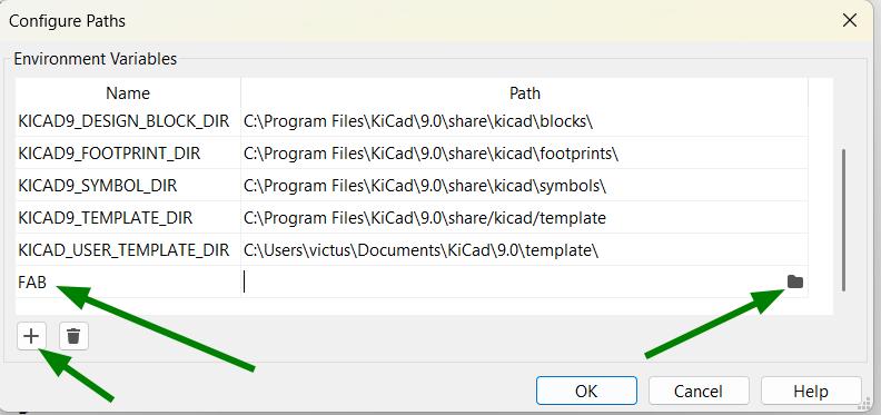
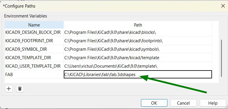
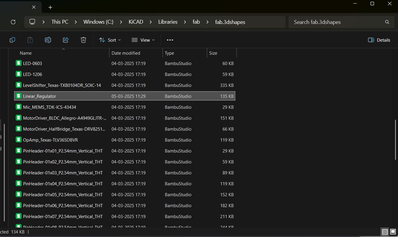
After all these I tried 3D viewer. For that I need to add the Environment variables inside KiCAD. For that Preferences → Configure Paths → Add a new environment variable and specify the path of the folder in which the 3D files are.
 |
 |
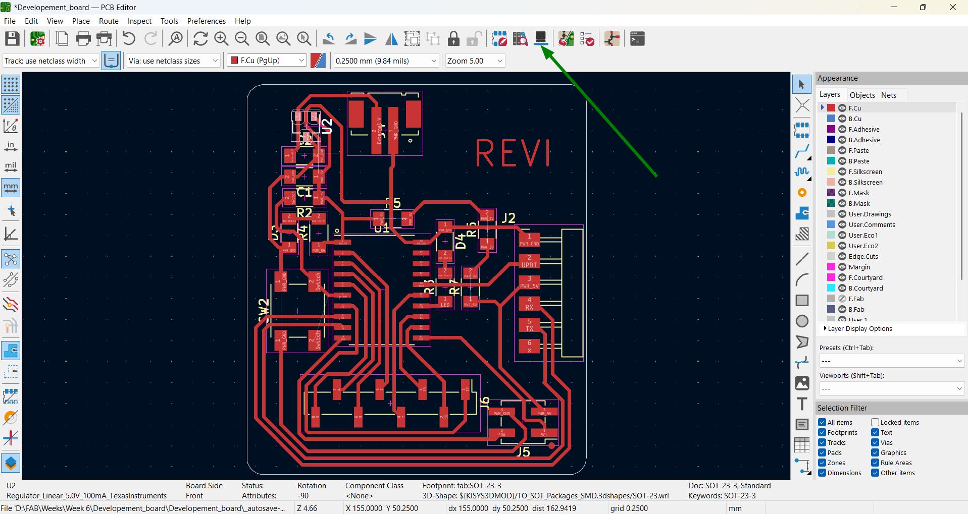
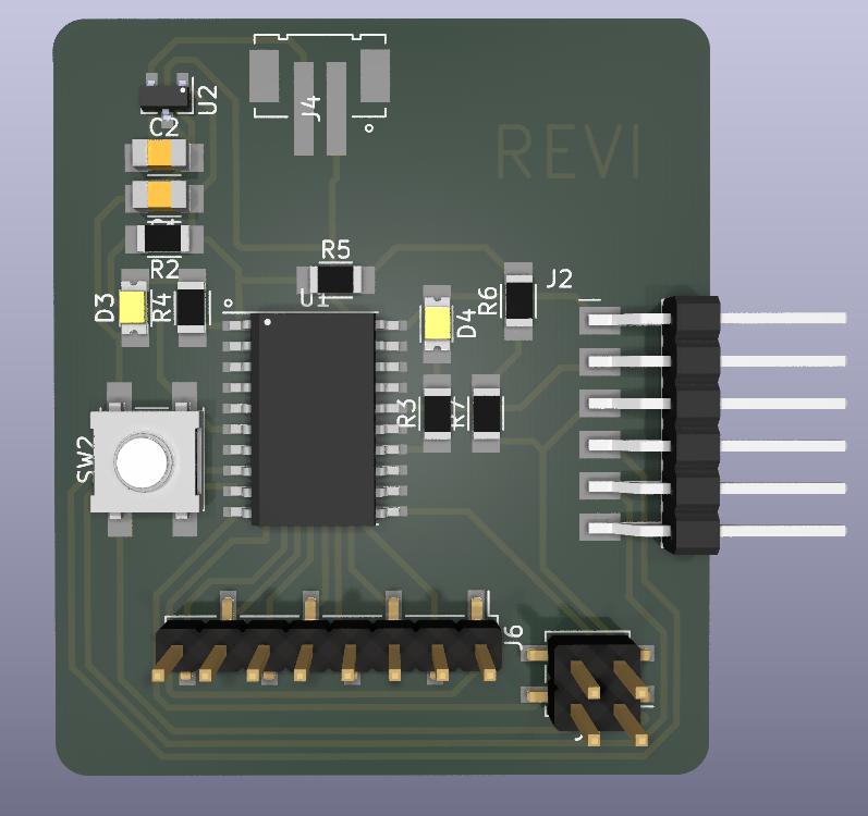
After adding the environment variables I opened the 3D viewer from Pcb editor and the 3D model of my PCB looks like this.
 |
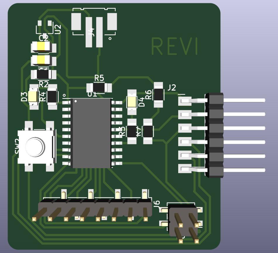 |
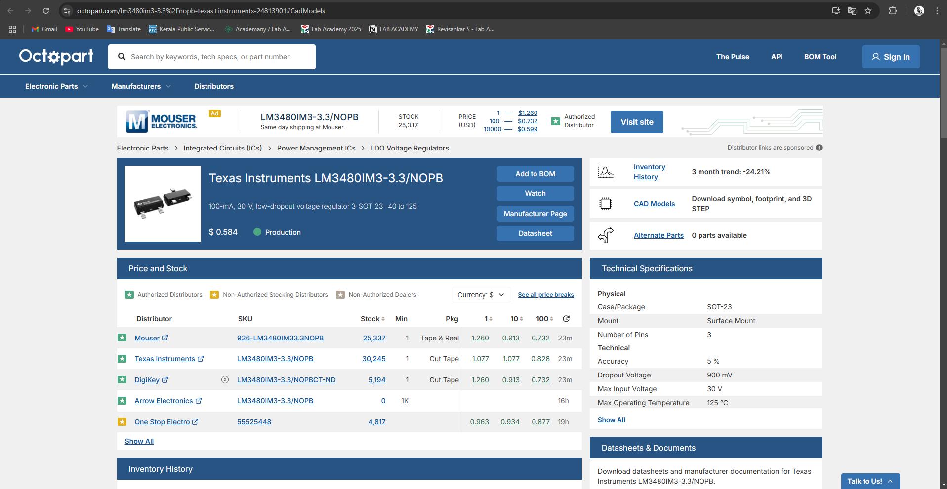
In this 3D model 2 components were missing and I tried to add these from external source. while searching in web I got the linear redulator 3D image but I didn't get the JST connector. For adding external components I followed these steps,
- Downloaded the 3D model from Octopart.
- Pasted the file inside folder where the 3D files are present.
- The 3d file was inserted in the 3d model.
Exporting file
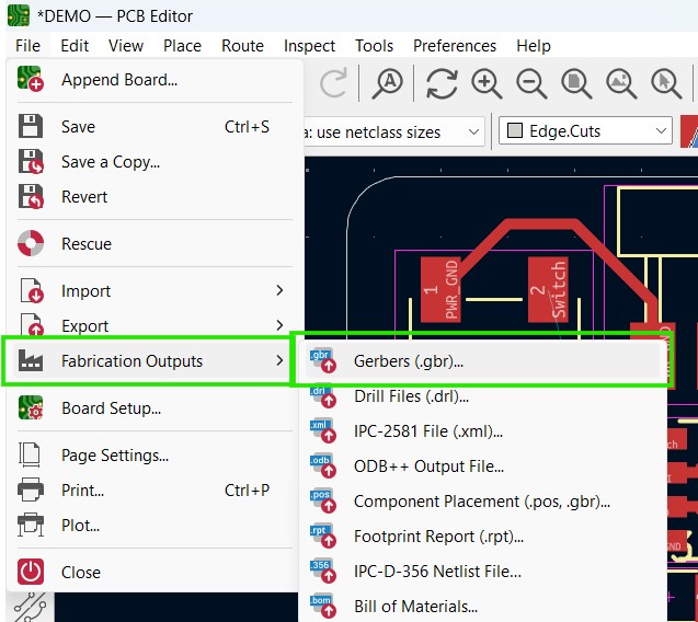
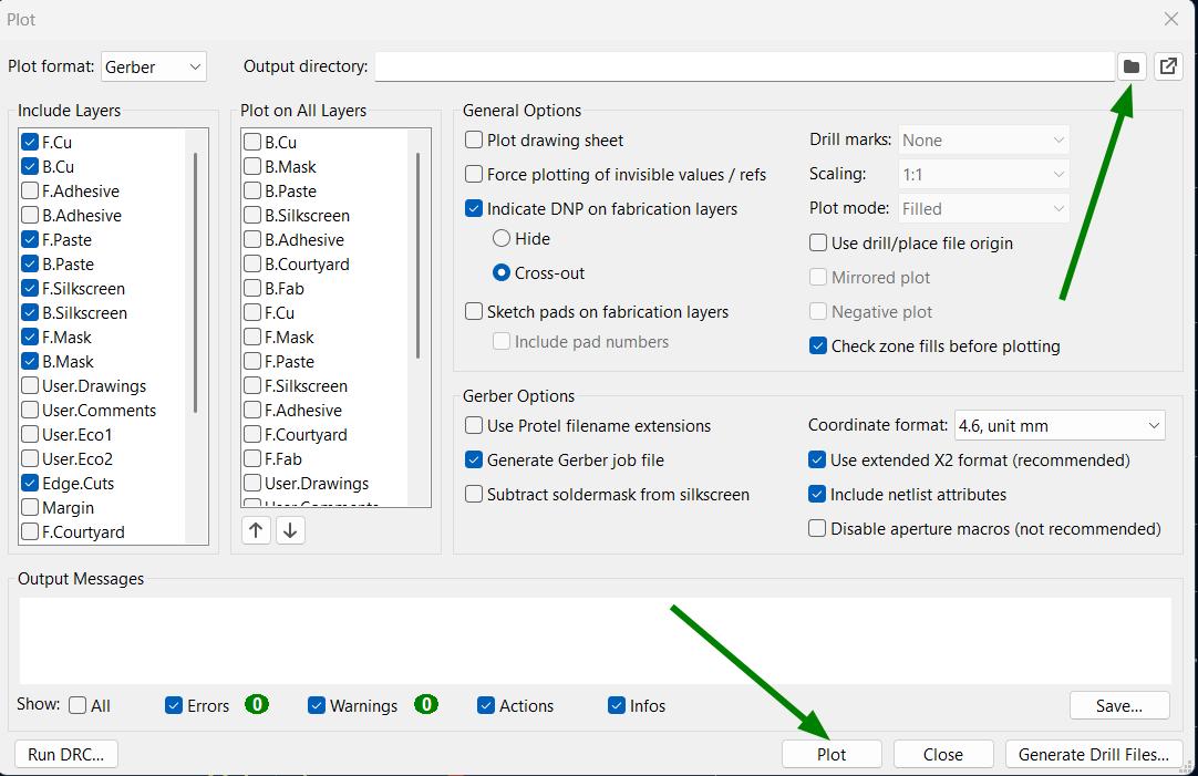
After designing the PCB I exported the file as .stepand .gbr.
To export the file as .gbr, File→ Fabrication Outputs→ Gerbers. Selected the folder to save the .gbr file and click plot to export it as .gbr.
 |
 |
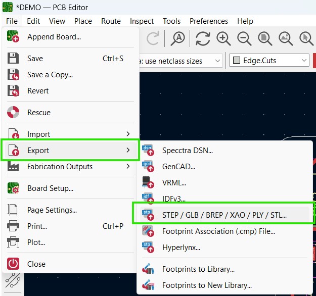
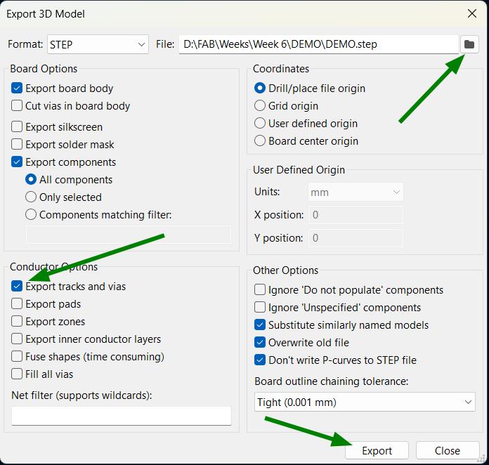
To export the file as .step, File→ Export→ STEP/ GLB/ BREP/ XAO/ PLY/ STL. Select the output folder and select Export tracks and vias by default it will be turned off. It was to export the tracks as well in the .step file. Then select export.
 |
 |
Hero Shot
 |
 |
Conclusion
In conclusion, this week provided valuable insights into electronic components, including both passive and active types. I also explored EDA software, focusing on KiCAD for PCB design. As a practical application, I designed a simple development board using the ATtiny3216 microcontroller.