Design and produce something with a digital process
(incorporating computer-aided design and manufacturing) not covered
in another assignment, documenting the requirements that your
assignment meets, and including everything necessary to reproduce
Pick and place
For wildcard week i decided to explore how to use and operate a pick and place machine. Using this machine will
also coincide perfectly with my final project. Since i am making multiple modular nodes that will be in the same
configuration in terms of the electronics part,it might make my job easier and faster.
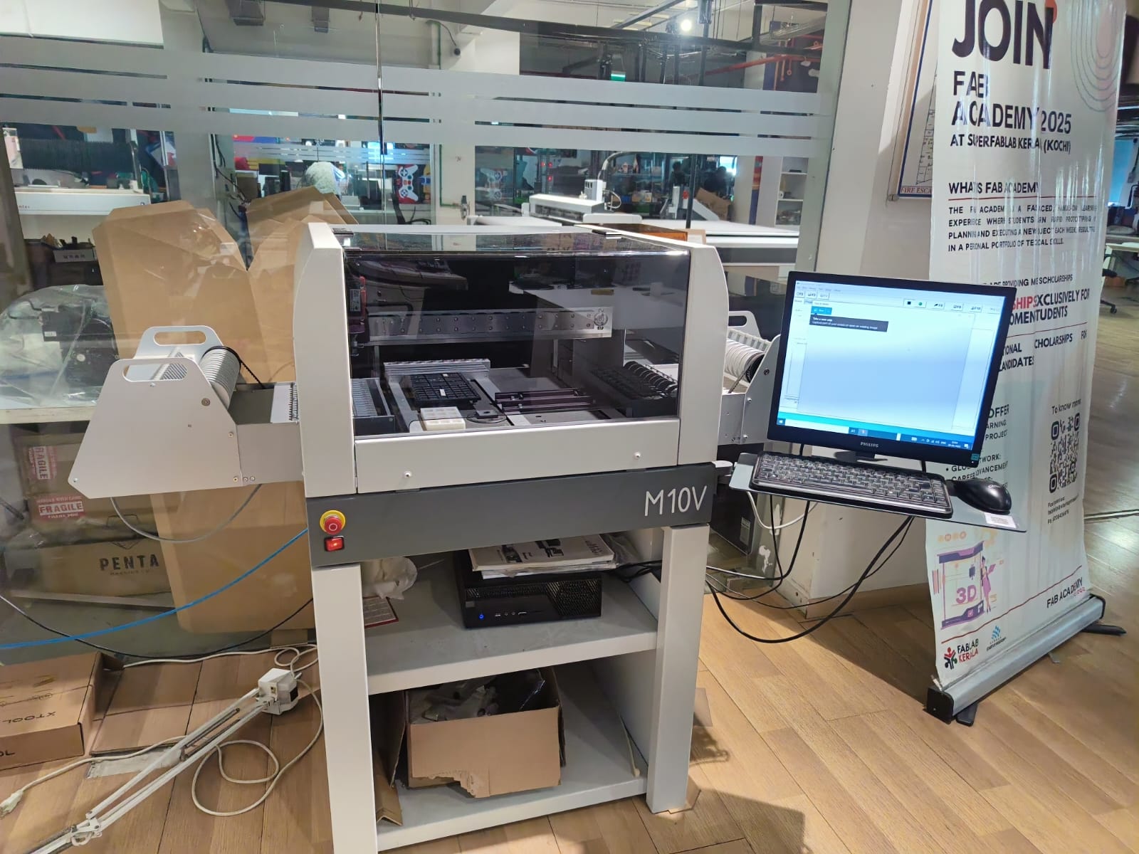
M10V
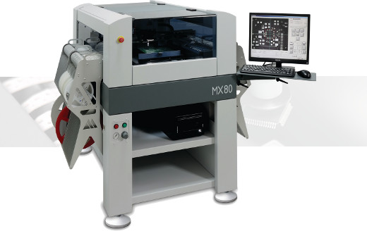
The pick and place machine we have at our lab is the Mechatronika M10V.
The Mechatronika M10V is a pick and
place machine designed for automated SMD component placement. It's known for
its versatility, ability to handle bulk (loose) components, and inclusion of a vision system for precise
alignment. The M10V can place components from 0201 to 40x40 mm, making it suitable for prototyping and small-scale
production.
Features:
Vision Centering
Fully automated placing
Automatic fiducials correction and bad mark sensing
Automatic change of nozzles
Automatic feeding of bulk / loose components
Pick & Place data can be entered manually in TEACH-IN mode or can be converted from various CAD data systems
Good price to performance ratio.
Sources Referred
The main and only documentation i referred to understand how to operate the machine was from the channelengineer's
videos on the M10V machine. His videos give a through and proper understanding on how to use the machine , the
software and the parts of the machine.It is a 5 part series by the end of which you get a good idea on the
procedures.
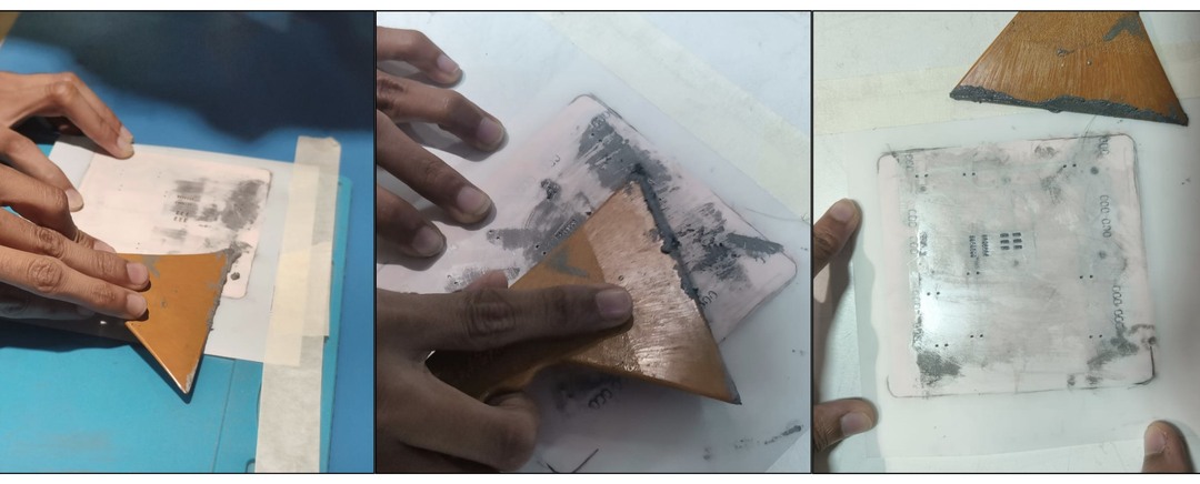
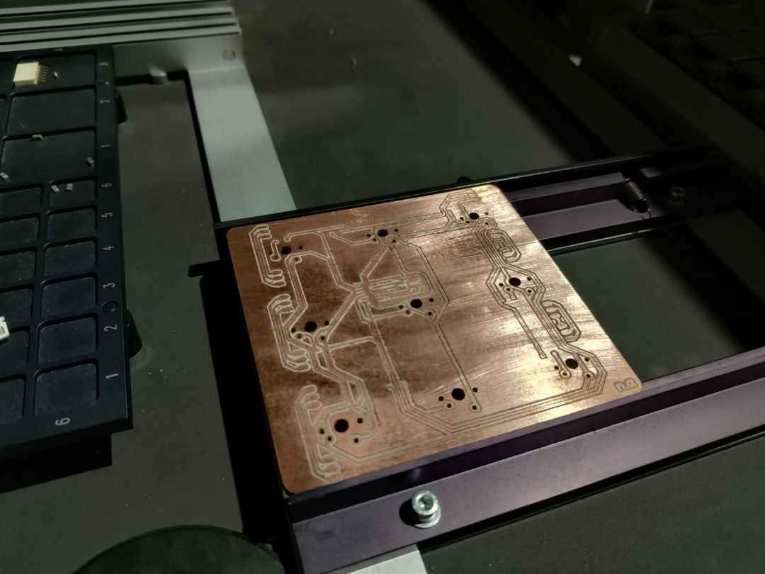
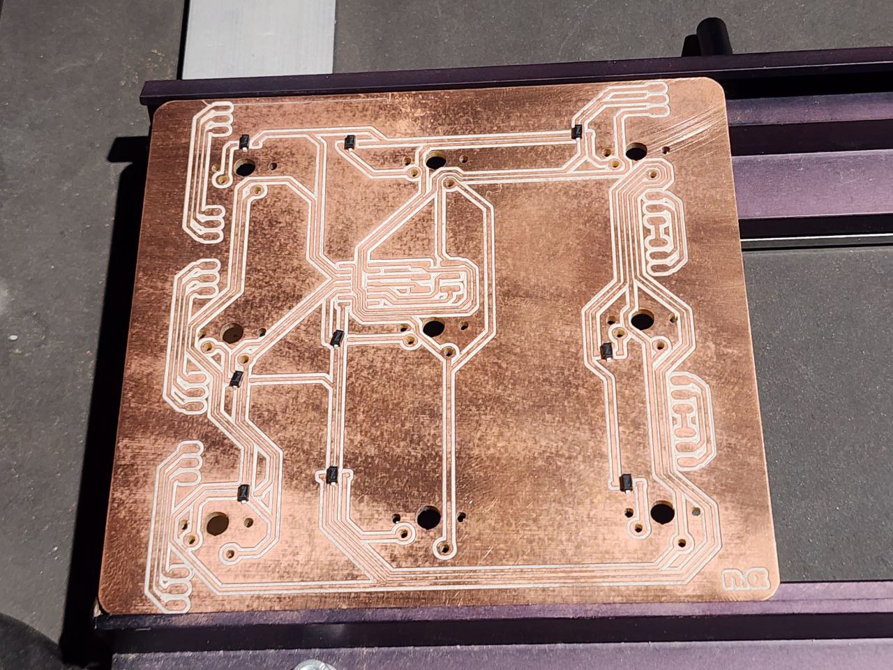
Preparing the PCB
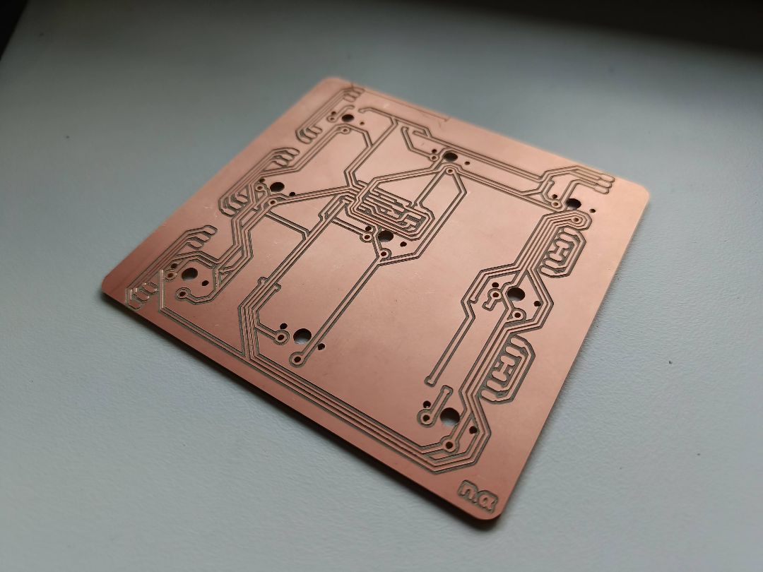
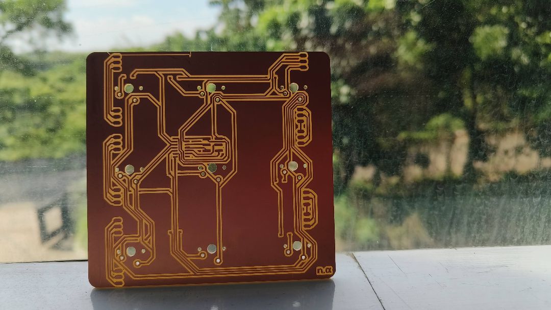
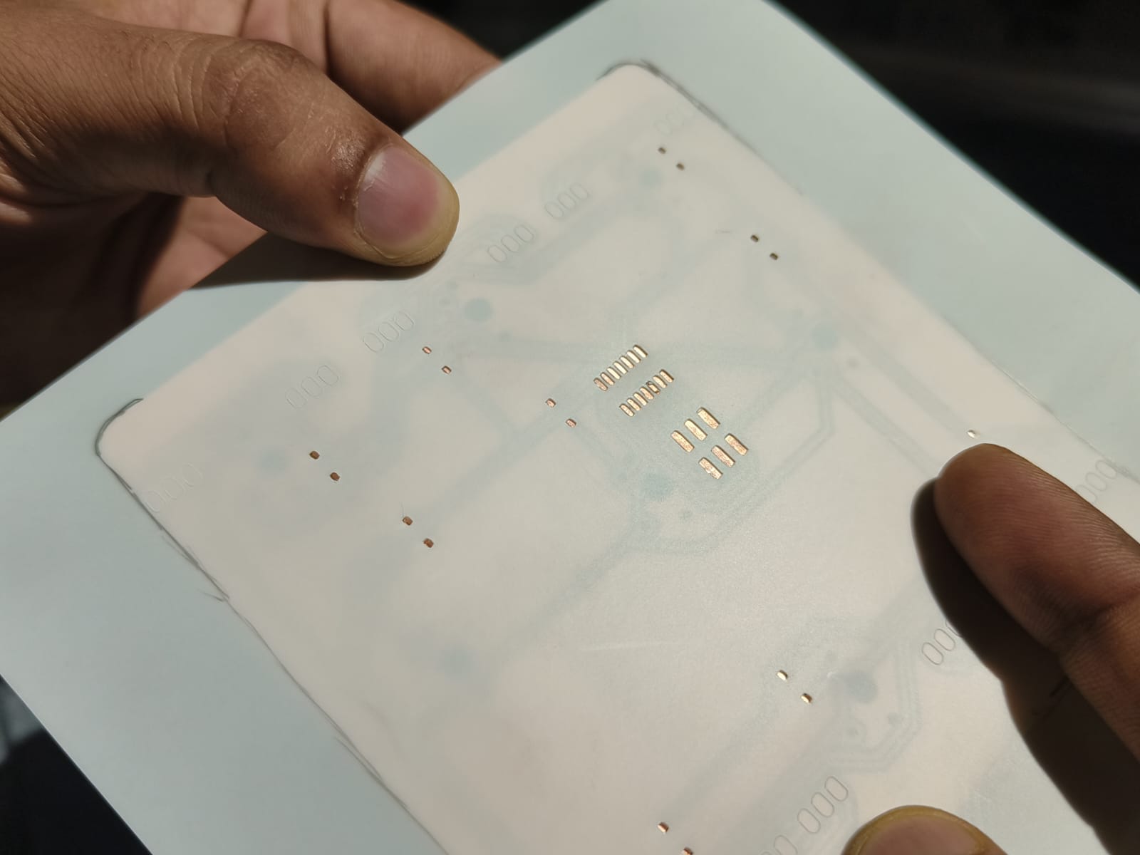
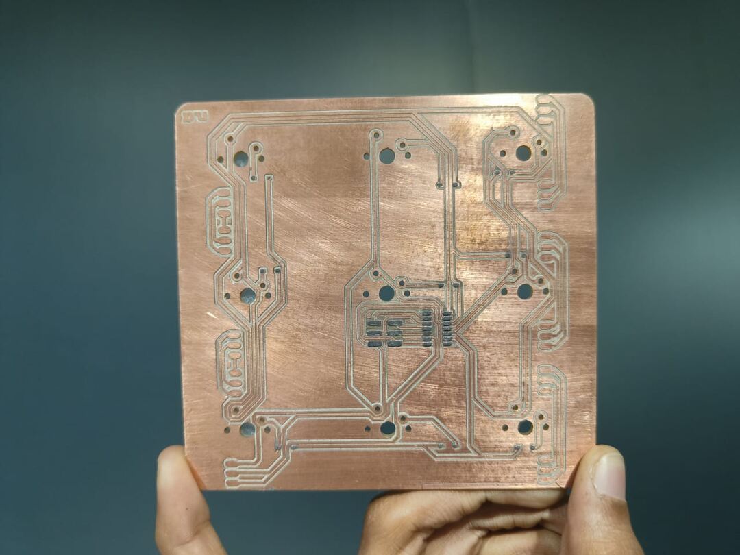
I had designed a PCB for the Nodes in my final project in KiCAD.
Then it was milled out and kept ready for this assignment.
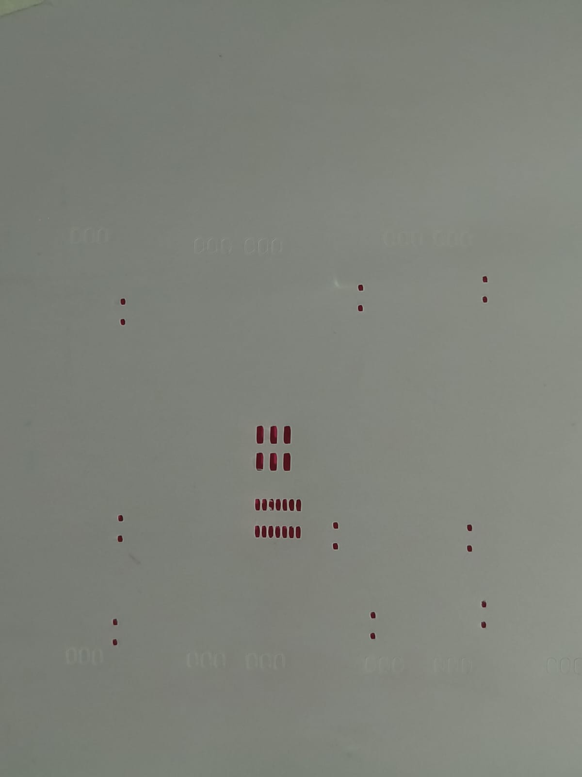
I also had to prepare a stencil of the pad postions to apply solder paste as the solder dispensing system was
not working.
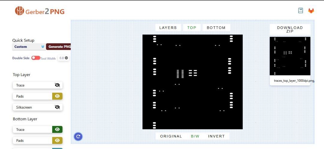
In gerber to png there is an option to get the traces and the pads separately .
The stencil was cut out of sythetic paper using the vinyl cutter. The sythetic paper used for the stencil was
the leftover roll from Kalyani's
final project from last year.
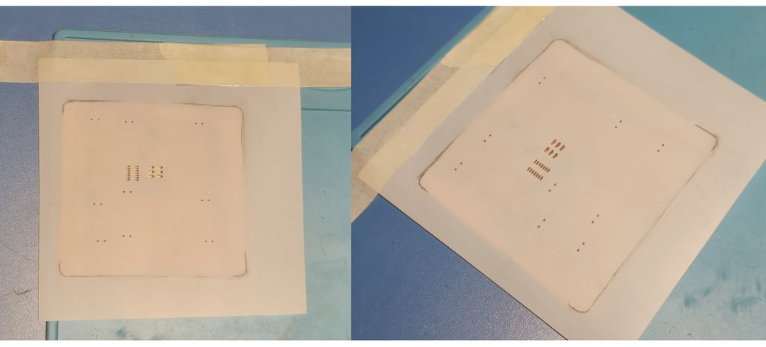
Then fix the PCB securely with some tape as it shouldnt move while the paste is being applied.
Align the stencil over the pads correctly. Put some solder paste at one side of th estencil and then using a
squeegee or a card firmly spread the paste across the board.
Remove any excess paste and lift the stencil carefully without disturbing spreading the applied paste.
Operating the machine
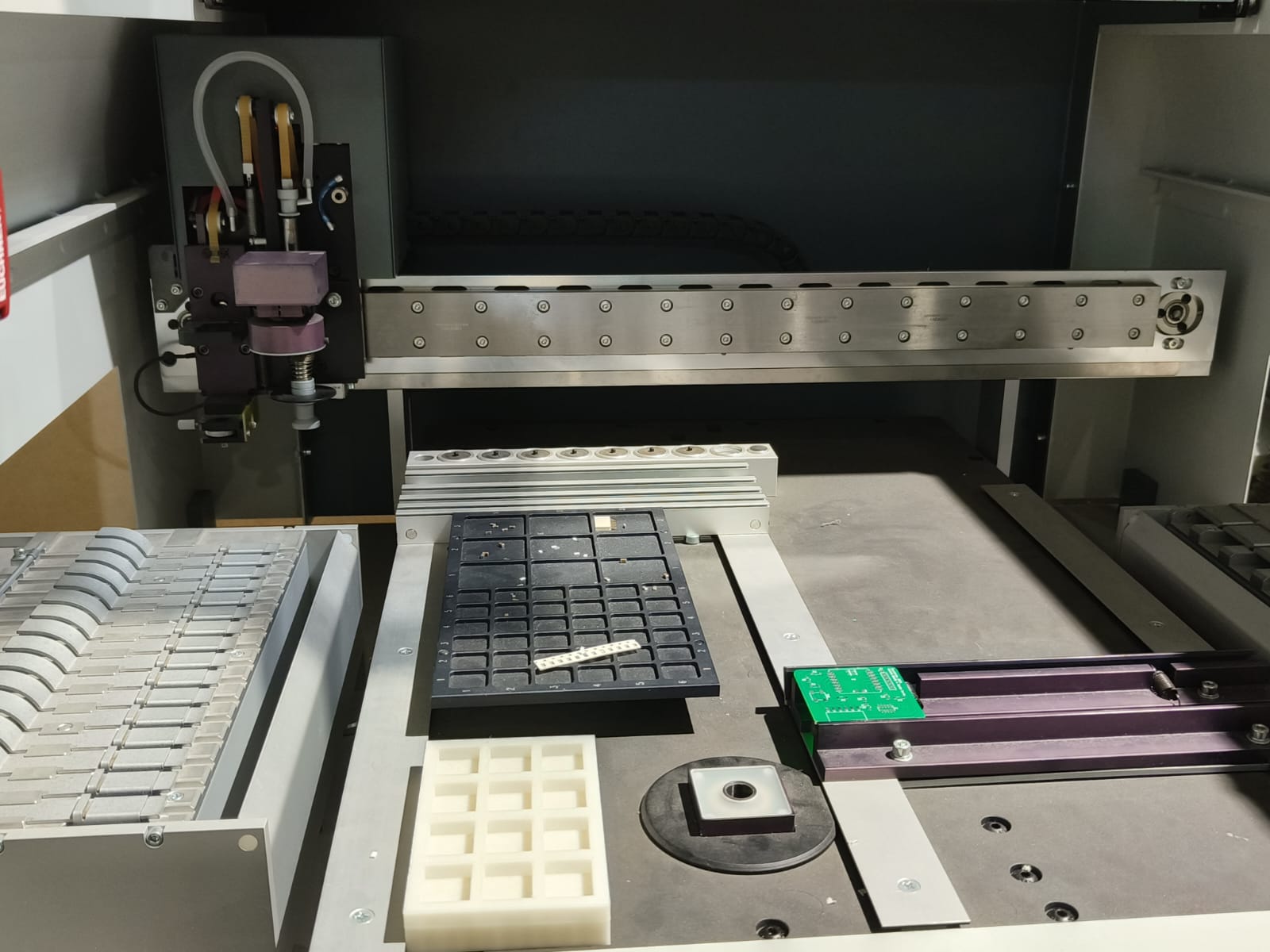
Placing the PCB & Components
Place the board securely in between the plates towards the left end and tighten the nuts.
There were 3 types of components i had to place : Diodes, Attiny1614 and vertical SMD Pin Headers
Machine Setup
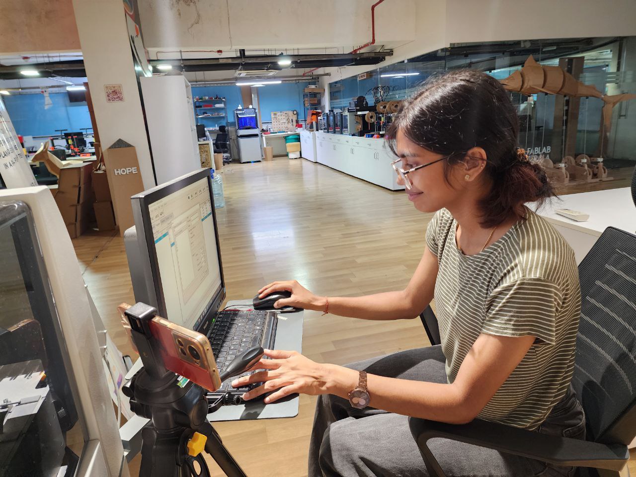
Setting up the Software
Open the mechatronika software.
Name the file under the author field.
You can see the various tabs such as :
Board
Program
Feeders
System
Log
These are required for operating the machine which we shall follow step by step.
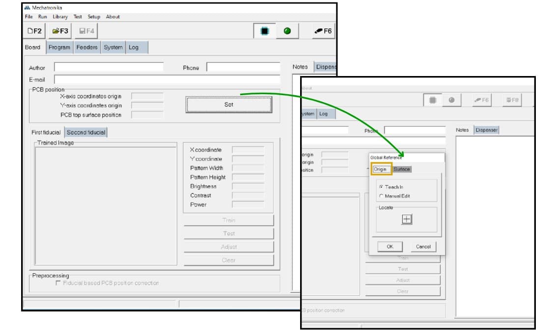
Setting the board origin
The first thing we have to do is to set the origin points of the PCB. Go to the Board tab and click on 'Set.'
A global reference dialogue box appears . Click on teach in and press on the '+' button.
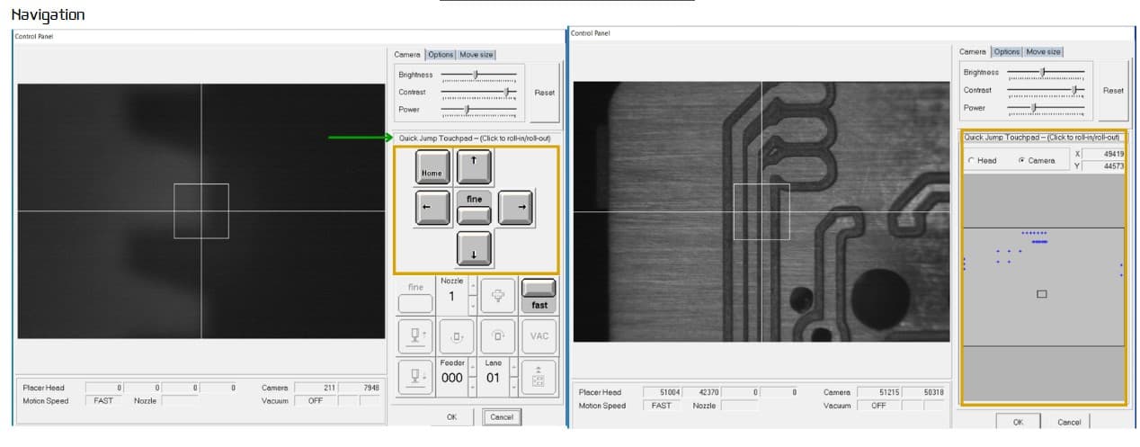
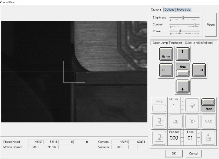
A window opens up showing the camera and nozzle position. Using the arrow keys and the coarse and fine button
navigate the crosshair the bottom right edge of the PCB. You can also use the quick jump toggle option to move
across board by clicking on the bed area.
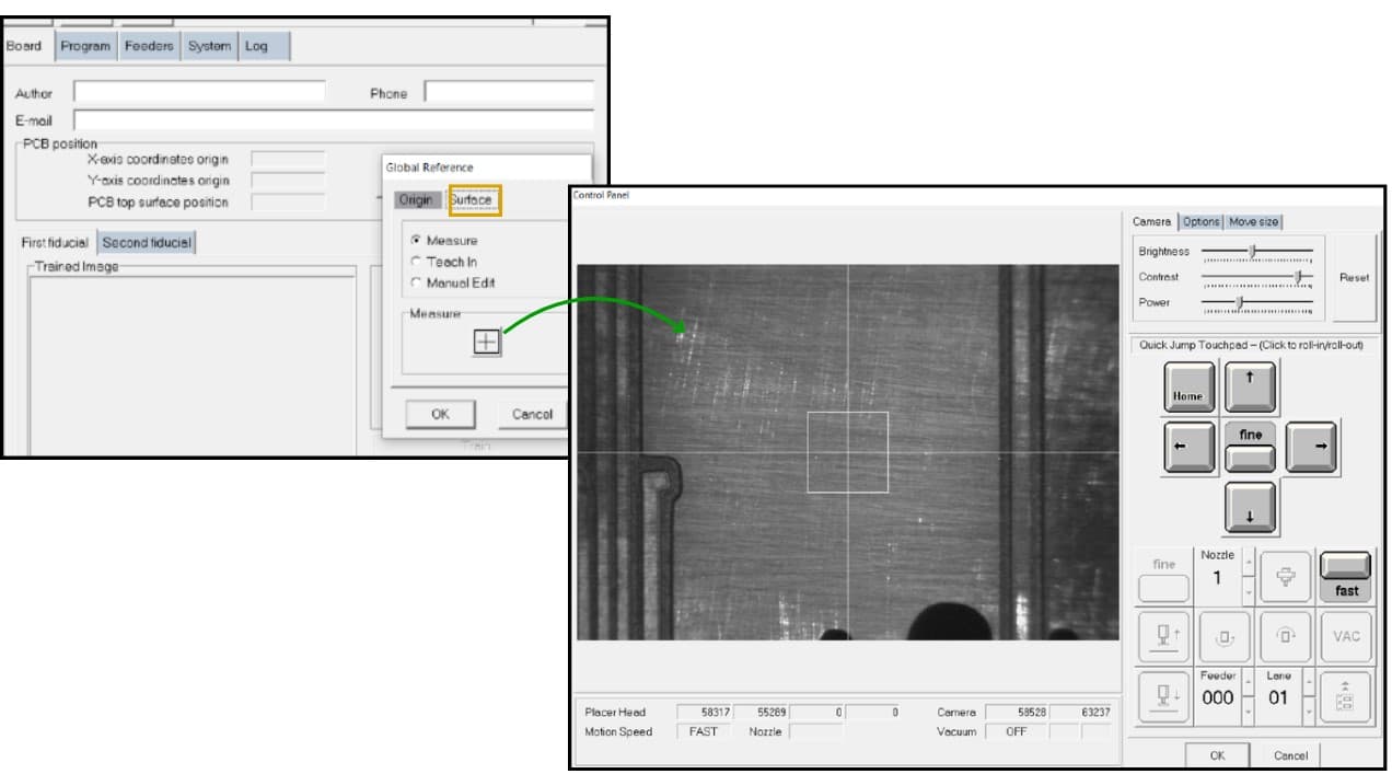
Once the origin is set click on OK.This will take you back to the global reference dialogue box. We have to
choose the Surface option next to set the Z level. Click on measure>> ok.
The control panel opens up. Navigate the pointer to an area on the PCB(preferably on the center) where there
are no holes or pads and then click OK. The machine will automatically set the level.
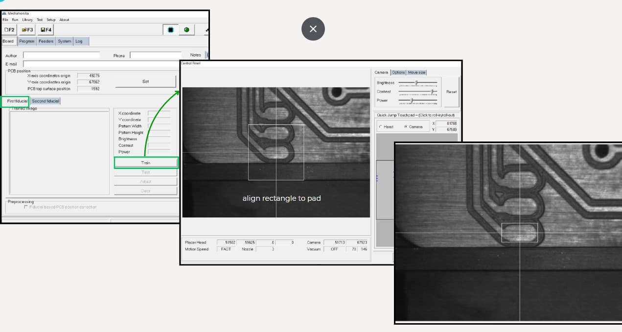
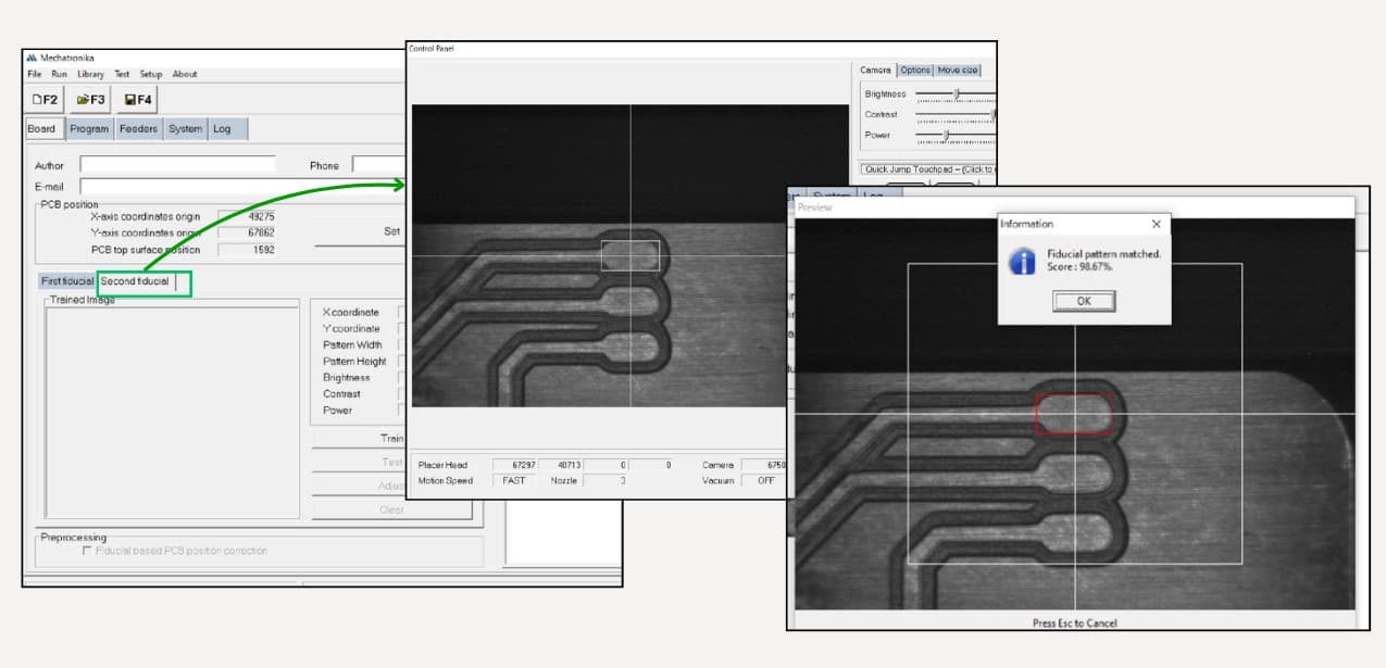
Once that is done go to the first fudicial tab. Click on Train. Navigate the pointer to a pad that is at the
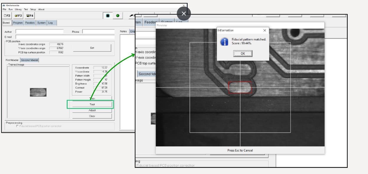
bottom left corner and adjust the rectangle on the point to coincide with the pad size. Click Ok. You can run a
test to check if the position is correct or not.
Next we can move on to the second Fudicial tab. Reapeat the same process as followed for the the first
fudicial.
Adding the components
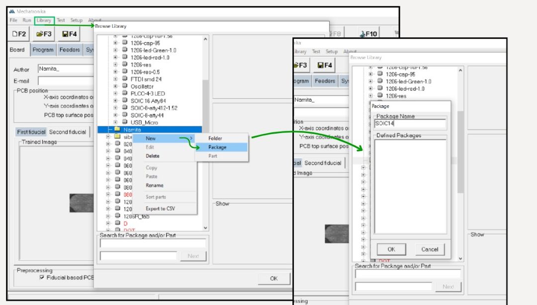
We need to load the components required into the software. Go to library and create a folder in your name.
Then right click on the folder and go to package. Give the name of your component and then click OK.similarly
create the packages for each component.
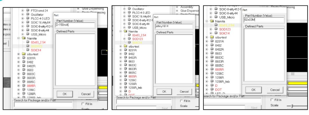
Next right click on the package and choose part. Here is where we set the dimensions of the components ,
Nozzle sizes and positions.
Under specifications we have to enter the dimensions of the component. I measured it using vernier calipers
and then entered the values into the respective fields. If the component has a polarity check on the polarity
box and mark the position at 0 rotation.
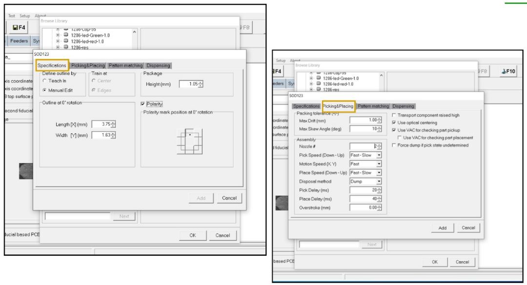
Next go to the Picking &Placing tab and set the nozzle size according to the component. Here for the
attiny1614 i choose 5 as the nozzle. Click Add. We will come back to this dialogue box in a bit to set the
pattern matching .
Feeders
Under the feeders tab you will see the lanes and their designated numbers. We need to assign which
component lies where in the tray/reel
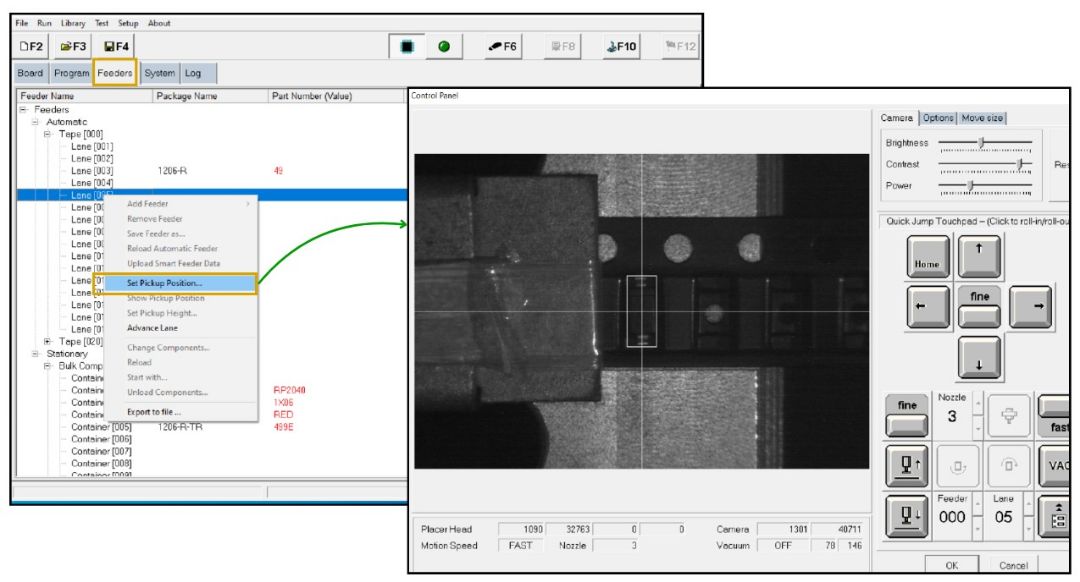
Select the tray/strip/lane that your component is in. Right click on the name and click "Set Pickup
Position."
The control panel dialogue opens up. Set the cursor to wher the component is exactly and align the
rectangle to the component
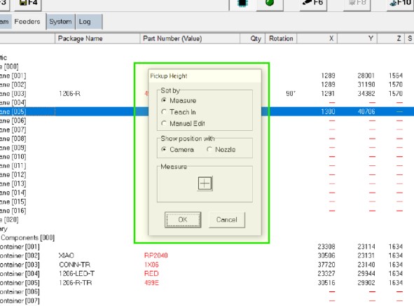
Back in the feeders tab right click again and click "Set Pickup Height". Mark "measure" and "camera" and
click on +.
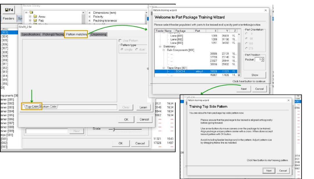
Now here is where we go back to the pattern matching tab under library I mentioned we will come back to.
Go to library>> choose the part to set. For the ease of explaining i will explain how i did this for the
attiny1614.
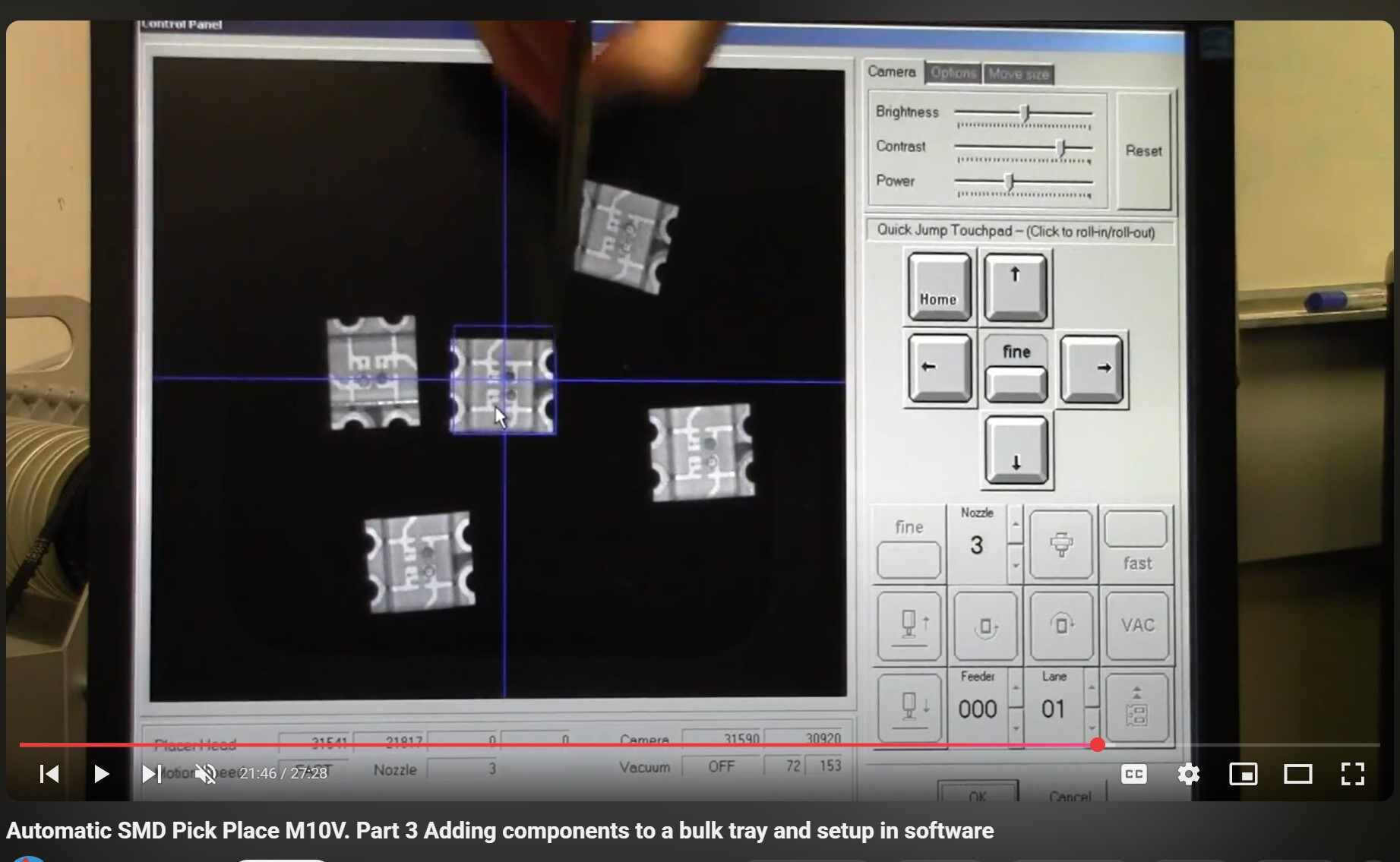
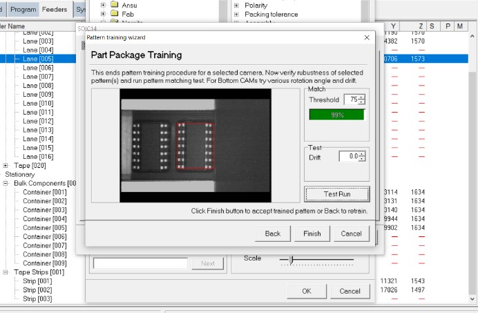
Go to pattern matching> Top Cam>> Learn. A part packaging training Wizard pop up opens. Click on the
component and press 'Next'. Verify if the image shown is correct and click next. This will take you to
Training pattern. Click on test run and do some runs by setting small drift changes. If the test run match
is above 76% you are good to go. Click on Finish.
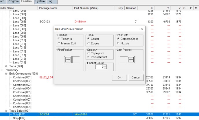
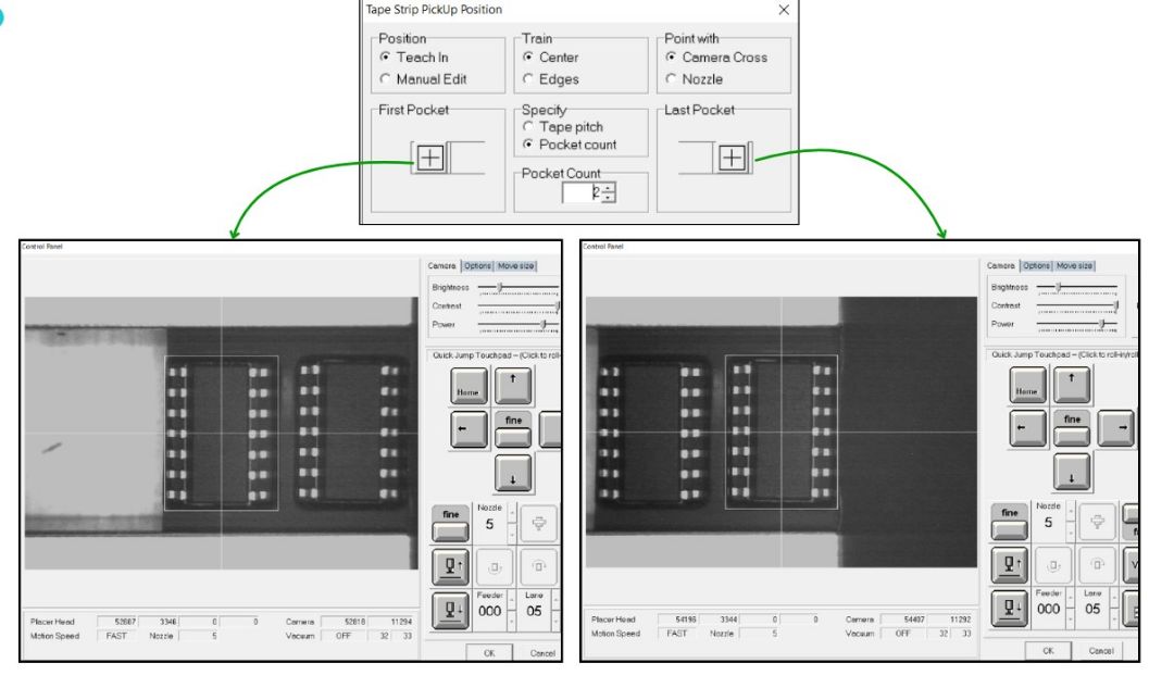
Since the Attiny1614 is on a tape Strip we need to set the begining and end of strip and the number of
pockets on the stip. I set the pocket count as 2 as there were only 2 pockets on the strip. Set the first
pocket location on the camera as well as the last one.
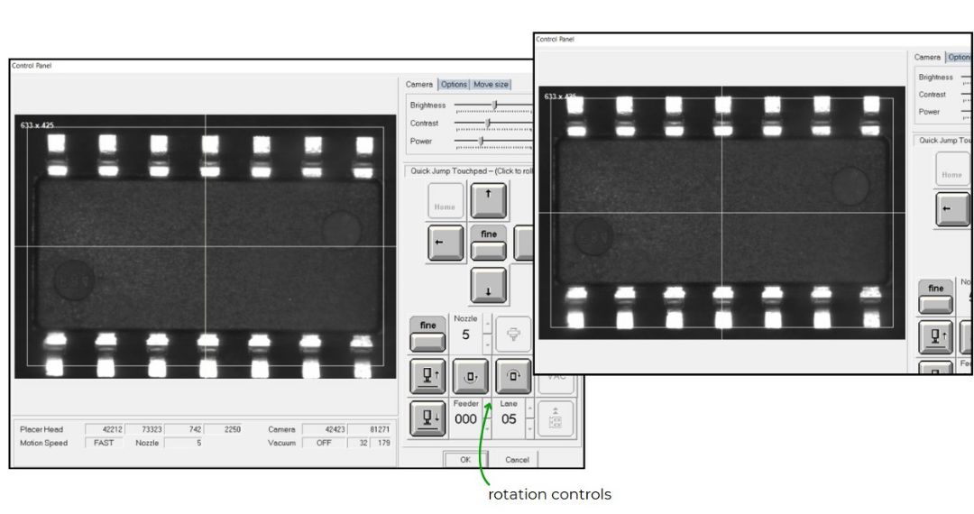
Now go to Bottom Cam. align the part to fit into the rectangle. If the part is at an angle rotate it and
make it straight.
Do some test runs again to verify the match.
A veritical header pin was one of the components i had to place on my board. But maybe because of the
height or size the nozzle was not picking it up and it came as and error.
The same process is repeated for the rest of the components . and then i moved on to program.
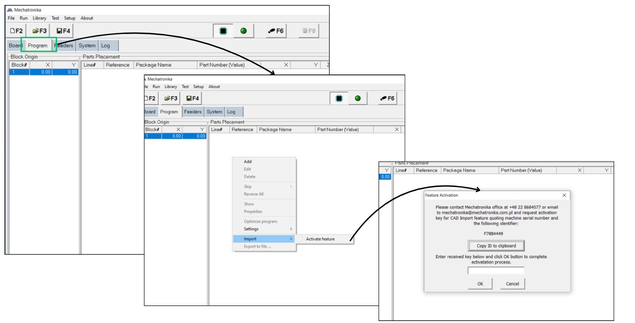
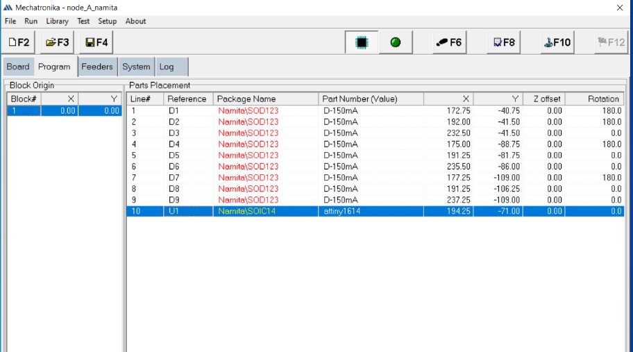
Program
I had exported a .pos file from KiCAD to be imported into the mechatronika software. A pos file has the
cordinate positions of the each of the parts. But unfortunately the software required a license key to
activate the import feature and we had to send a request to the company to send a key.
As an alternative i had to individulaly enter each component and their positions.
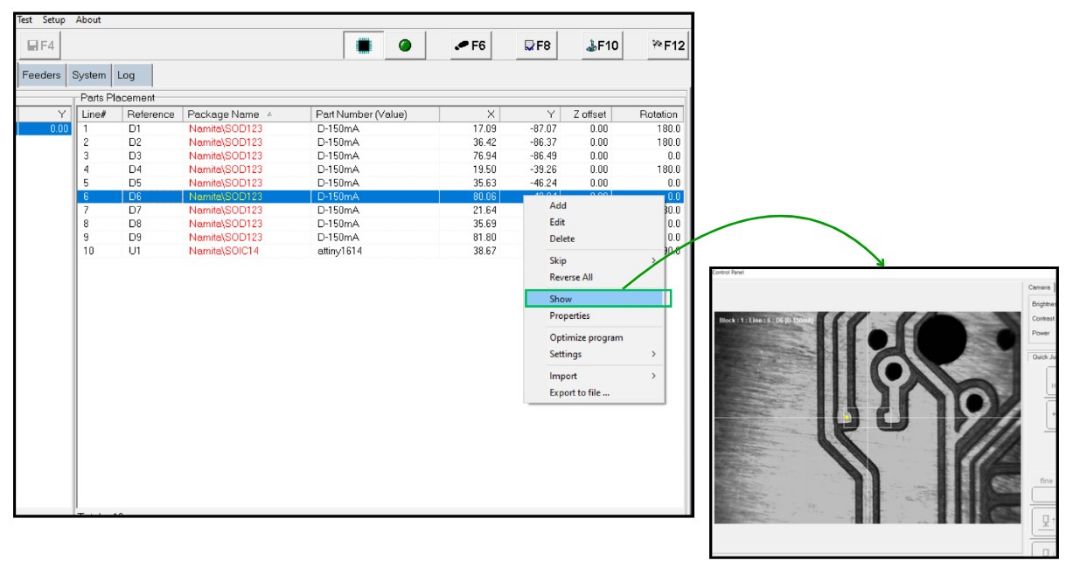
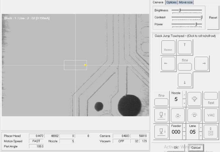
To check if the positions are entered correctly , right click on the part and go to "Show". The camera
will show where it is positioned at.
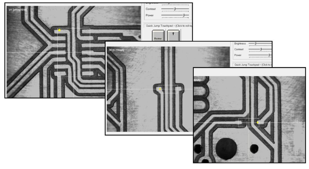
There was a mismatch in the positions and it was not aligning correctly.
to resolve this i went back into the kicad software to check if anything else was on the workspace. The
hidden items were deleted and the file was exported again, but it still did not align properly. So we had
go ahead and set each component place on the PCB manually.
Finally we can run the the program. Make sure the componet placing is selected and click F12 .
The machinne was able to pick the diodes and placed them correctly on the pcb. The attiny did not get
placed due to some issue that we are trying to fix.
Operating the machine after obtaining the license for the software.
All the steps followed above remain the same until the program section.
As i got the license of the software after sending an email to the company through our lab, I was able
to acess the features of the software such as obtaining the positions of the components on the board
directly from Kicad as a .pos file. This eliminates the need tomanually write down all the positons.
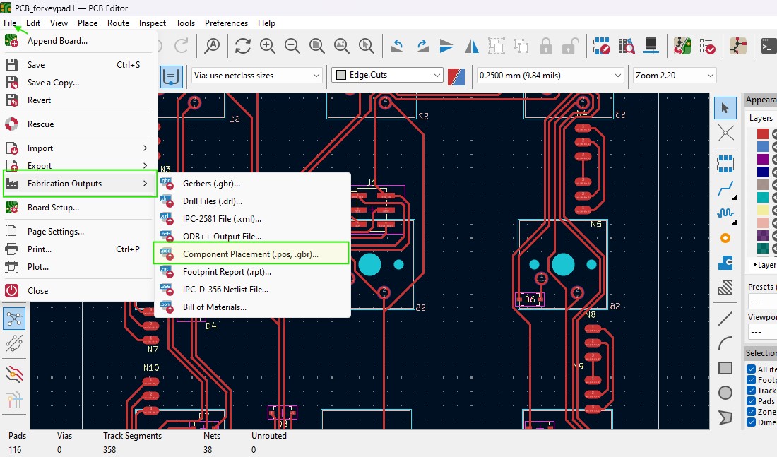
Exporting from .csv file KiCad
We need to to export the .pos file from KiCad. It is a footprint position file that contains
information about the placement of components on a PCB
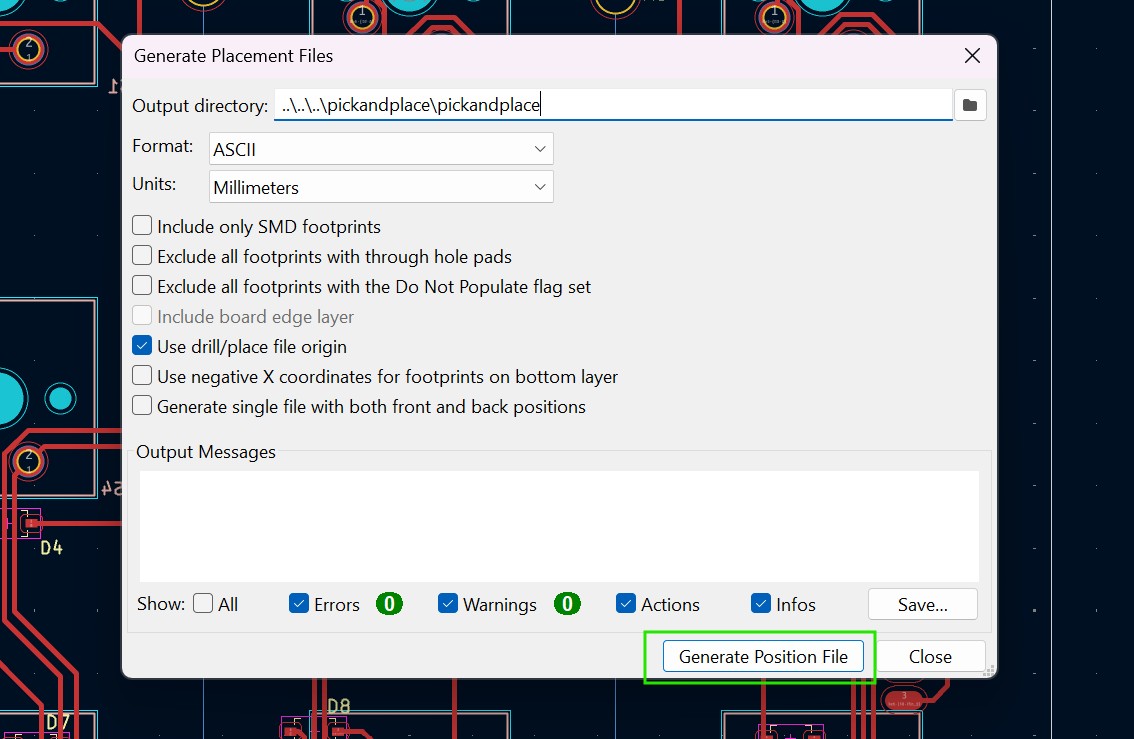
In the PCB editor window , Go to File >> Fabrication Outputs >>> Footprint Position (.pos)
Click on Generate File.
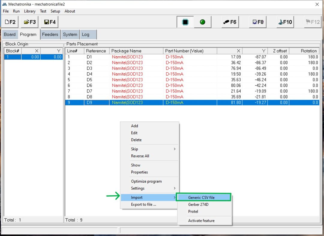
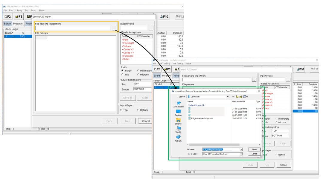
Importing .csv into Mechatronika software
Now we can got to the Mechatronika software and then go the program tab. Right click on the workspace and click on 'Import'.A dialogue box appears where you can import your files .
Select the file that you would like to import.
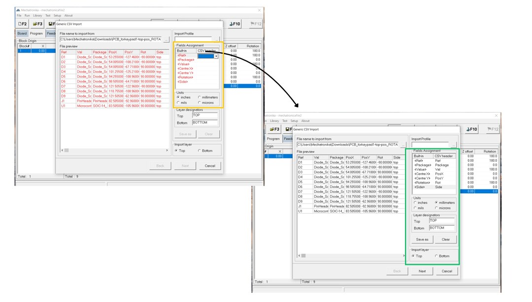
Now we have to match the built in fields to the .csv file fields to ensure everything is in the proper order. Make sure the units are the same as it was in the Kicad file. I had kept it in milimeters.
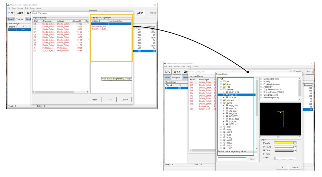
After that is done click on next. Here we have to match the packages witrh the names in the csv file. Then click next
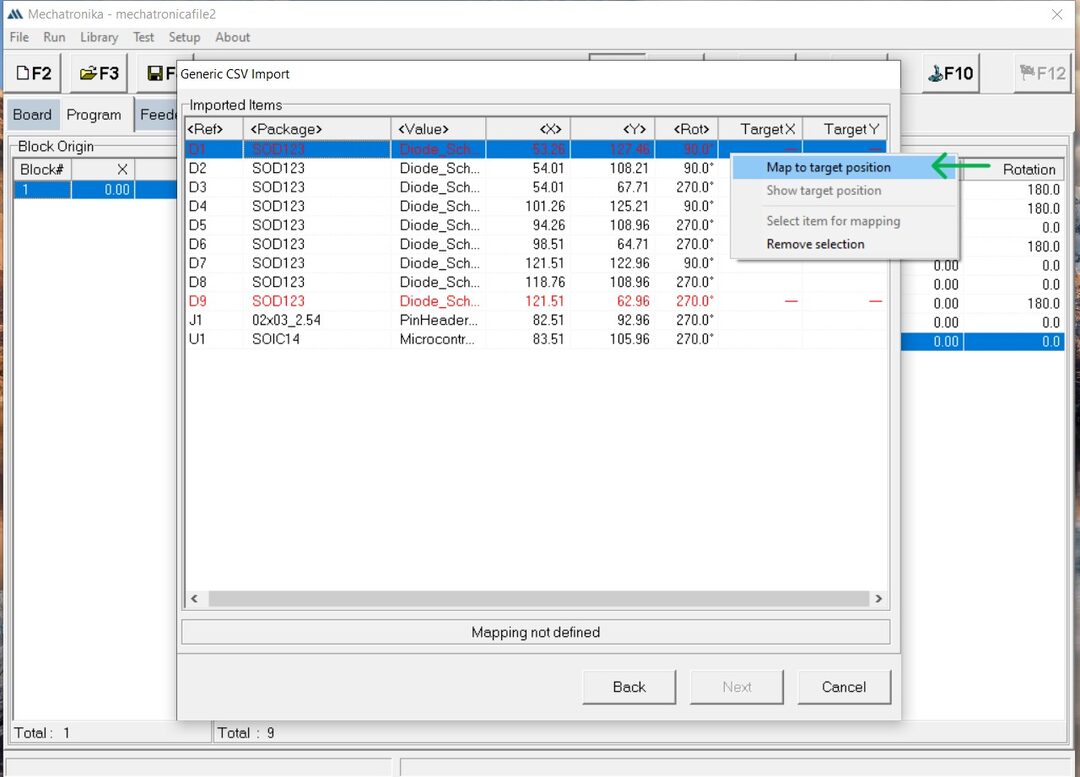
Now all the elements are loaded . In the case that some appear red right click and select Map Target area. This opens up the control panel where you can map the positon cordinates of the components.
Once everthing is cleared click OK and all the component positions are loaded into the program. This method was easier than manually typing in everything.
After checking everthing we can Run the program (F 12 ).
Reflow soldering
Reflow soldering is a process used to connect electronic components to the PCB by
melting solder paste using a controlled heat source.
After the components are placed, carefully take the PCB to the soldering station without any movement
that would shift the components.
Heat was applied evenly over the assembled PCB using a heat gun until the solder melts. Make sure not to
keep the heat gun at one place for too long as it may damage the components.
After the components are soldered let it cool down.The PCB was inspected under a microscope to make sure
all connections were properly soldered on.