Week 6: Electronics Design
Table of Contents
This week was about getting familiar with the design of printed circuit boards (PCBs) using electronic design automation (EDA) software. Our task was to design a development board for an MCU. Besides that, we introduced ourselves to electrical measurement devices in the lab.
This week we got introduced to PCB design, but we also used it in the following weeks and learned a lot more then. For more PCB design, check all other weeks with the tag kicad.
This Week’s Tasks
- Group assignment:
- Use the test equipment in your lab to observe the operation of a microcontroller circuit board (as a minimum, you should demonstrate the use of a multimeter and oscilloscope)
- Document your work on the group work page and reflect what you learned on your individual page
- Individual assignment:
- Use an EDA tool to design a development board that uses parts from the inventory to interact and communicate with an embedded microcontroller
- Extra credit: try another design workflow
- Extra credit: simulate your design
- Extra credit: design a case around your design
This Week’s Board
In the following pictures you see the traces of the board, I designed this week as well as a pin-out diagram of a XIAO ESP32-S3. This information I would need to access quickly in the following weeks, so I put it on top.


Introduction to the Electrical Measuring Equipment
This group assignment we did on Thursday in the morning. For the documentation, pictures where taken by Richard and assembled by me. Benedikt wrote the description text based on his knowledge and partly on my notes. I then adapted Benedikt’s documentation, partly with changes for this page. The group assignment can be found here
Setup
For testing purposes, we used an Arduino Nano with the “Fade” example code from Arduino. This generates a PWM signal on pin 9, cycling in five steps from 0% to 100%. The signal should oscillate between < 0.8V and > 3V, with VCC being approximately +5V.
 1/*
 2  Fade
 3
 4  This example shows how to fade an LED on pin 9 using the analogWrite()
 5  function.
 6
 7  The analogWrite() function uses PWM, so if you want to change the pin you're
 8  using, be sure to use another PWM capable pin. On most Arduino, the PWM pins
 9  are identified with a "~" sign, like ~3, ~5, ~6, ~9, ~10 and ~11.
10
11  This example code is in the public domain.
12
13  https://www.arduino.cc/en/Tutorial/BuiltInExamples/Fade
14*/
15
16int led = 9;         // the PWM pin the LED is attached to
17int brightness = 0;  // how bright the LED is
18int fadeAmount = 5;  // how many points to fade the LED by
19
20// the setup routine runs once when you press reset:
21void setup() {
22  // declare pin 9 to be an output:
23  pinMode(led, OUTPUT);
24}
25
26// the loop routine runs over and over again forever:
27void loop() {
28  // set the brightness of pin 9:
29  analogWrite(led, brightness);
30
31  // change the brightness for next time through the loop:
32  brightness = brightness + fadeAmount;
33
34  // reverse the direction of the fading at the ends of the fade:
35  if (brightness <= 0 || brightness >= 255) {
36    fadeAmount = -fadeAmount;
37  }
38  // wait for 30 milliseconds to see the dimming effect
39  delay(30);
40}
Power Supply & Multimeter
General work advice for working with the power supply: before disconnecting any components, always gradually reduce voltage and current. When using a power supply, the LED indicator will be green in Constant Voltage (CV) mode and red in Constant Current (CC) mode. If it switches to CC mode unexpectedly, check for issues like short circuits.
When working with the multimeter, turn off battery-powered multimeters after use to prevent rapid battery depletion. Low-cost multimeters may provide inaccurate readings. High-quality multimeters indicate low battery levels. Avoid changing the measurement range mid-series, as impedance differences may lead to inconsistent results.
Measuring 3V3 & +5V Pins
For this first measurement, we used a Fluke 117 multimeter, and for the second, a Rigol DM3068 multimeter, measuring between the GND pin and 3V3, +5V, and VIN. The Arduino was connected via a 30 cm USB 2.0 Type A to USB Mini cable to a laptop.


| Pin | Fluke 117 | Rigol DM3068 |
|---|---|---|
| 3V3 | 3.29V | 3.291V |
| +5V | 4.73V | 4.731V |
| VIN | 4.31V | 4.263V |
We powered the Arduino via USB from a laptop, leading to some fluctuations in power delivery. The laptop was running on battery power, and additional voltage drops occurred due to the cable and connection resistances. The probe wires used should have an impedance of 50Ohms. If powered via the VIN pin from a stable power source, such as a regulated power supply, the results would be closer to 3.3V and +5V. In this case, the LM1117IMPX-5.0 regulator would provide +5V, and the FT232RL would derive 3,3V from the +5V rail, requiring an input voltage between 7-15V, according to the Arduino data sheet.
Power Consumption of the Arduino
For this measurement, we switched to a GW Instek GPS-3303 power supply.


For convenience, we used the same setup to connect the Rigol DM3068 multimeter.

We measured -16,1890 mA. The accuracy of the multimeter is impressive, as confirmed by the data sheet. The negative value resulted from reversing the measurement leads. For power consumption calculations, we simply use the absolute value:
\[ 5\text{V} \cdot |-16.189 \cdot 10^{-3}\text{A}| = 80.945 \cdot 10^-3\text{W} \]
A similar measurement could be performed while powering the setup from a laptop, but it would be more complicated unless a USB cable is cut in half. This is because a multimeter in current measurement mode must be placed in series, and the input voltage from the laptop would also need to be measured. At this point, one could debate whether it is better to measure voltage or current precisely, or if simply using a power meter would be the more practical approach.
Oscilloscope
For the next measurement we needed to use the oscilloscope (osci). This is why I include a brief introduction to working with it here.


Brown-Out Point
The brown-out point refers to the voltage level at which the microcontroller shuts down due to undervoltage. For an externally powered Arduino Nano via the VIN pin, this test determines the minimum required voltage for the LM1117IMPX-5.0 regulator. The data sheet suggests that this point should be slightly below 7V. We confirmed microcontroller functionality using an oscilloscope.


The PWM amplitude remained between 4.9V and 5.1V above 6V supply voltage. Below 4.4V, the microcontroller shut down entirely, identifying the brown-out point at 4.4V.
PCB Design Rules
For getting to know about PCB design rules, I checked a document about that which was written by Benedikt some years ago. Additionally, I talked with Benedikt about good practices in general.
The first set of rules considered schematic design and placing of the components. When deciding which pins of an IC or MCU to connect and which not to connect, make sure to always connect the GND pins to the circuit’s GND network. This can ensure better thermal dissipation. It is to be made sure that components are placed so that soldering tin only needs to be put on one side of the PCB. That implies that THT parts (the ones with the legs) need to be placed on the opposite side of the SMD parts. Similar parts should be aligned all in the same way, that is if a resistor is aligned horizontally, all other resistors should be aligned horizontally. This is done for easier and faster placement, especially when automated placement machines are used. Additionally, care should be taken with the placement of components to prevent interference with one another. The soldering process is to be considered. In the case of wavesoldering it is required that smaller components are placed before larger ones (in the wave direction). For manual soldering, it needs to be kept in mind that larger components are soldered after smaller ones, ensuring accessibility for soldering iron tips. Components placed too close together can hinder proper soldering.
After placing the components, the conductor needs to be traced between the components. Those traces should be short and possibly direct. Traces which are expected to carry high-frequency (>300kHz) signals, must be routed at 45/135-degree angles. The angles are to be chosen so that the charge carriers (electrons) do not need to travel in sharp angles. I did not understand this to the fullest extent, since it is possible to have, e.g. a sine-wave signal, where the traveling direction alternates. Due to time constraints I put this question aside. I will consider it again, once I deal with high-frequency circuits. For now, I just take it as a good practice to have 45-degree angles. Trace widths should be adjusted based on current and temperature differences to prevent overheating and current damage. Power lines should be thicker than signal lines to handle higher currents without issues. A table considering trace width is written below. The symbol ΔT refers to the allowed temperature difference between the conductor and the surrounding matter. The table is only valid for a trace thickness of 35μm.
| Width [mm] | Width [mil] | I [A] with ΔT = 10 K | I [A] with ΔT = 20 K | I [A] with ΔT = 30 K | I [A] with ΔT = 40 K | I [A] with ΔT = 50 K | I [A] with ΔT = 60 K |
|---|---|---|---|---|---|---|---|
| 0.1 | 4 | 0.4 | 0.6 | 0.8 | 0.9 | 1.0 | 1.1 |
| 0.2 | 8 | 0.7 | 1.0 | 1.2 | 1.4 | 1.6 | 1.7 |
| 0.3 | 12 | 0.9 | 1.3 | 1.6 | 1.8 | 2.0 | 2.2 |
| 0.4 | 16 | 1.1 | 1.5 | 1.9 | 2.2 | 2.4 | 2.7 |
| 0.5 | 20 | 1.3 | 1.8 | 2.2 | 2.5 | 2.8 | 3.1 |
| 0.6 | 24 | 1.4 | 2.0 | 2.4 | 2.8 | 3.1 | 3.4 |
| 0.7 | 28 | 1.6 | 2.2 | 2.7 | 3.1 | 3.5 | 3.8 |
| 0.8 | 32 | 1.8 | 2.4 | 2.9 | 3.4 | 3.8 | 4.1 |
| 0.9 | 36 | 2.0 | 2.6 | 3.2 | 3.7 | 4.1 | 4.5 |
| 1.0 | 40 | 2.2 | 2.8 | 3.4 | 3.9 | 4.4 | 4.8 |
| 1.5 | 60 | 2.5 | 3.6 | 4.4 | 5.1 | 5.7 | 6.2 |
| 2.0 | 80 | 3.0 | 4.3 | 5.3 | 6.1 | 6.8 | 7.5 |
Another aspect to be considered is were to place the ground. The first option is to have traces for GND, just as for all other potentials. Alternatively, one could consider putting the GND potential onto larger islands of copper to lead all traces to. This island could e.g. be the residual copper area that surrounds the engraved traces when a PCB was milled. The first advantage is that it could be easier to do the tracing for such a configuration. Secondly, if you are dealing with high frequency (HF) signals on some traces, voltage could be induced in neighboring traces. This could induce a voltage in a trace that should be GND (i.e. where every two points on the trace must have the same voltage). If, instead, the GND node is a large copper plate, this effect could be minimized. Another advice for tracing is that you want to route all of your grounds going to one ground node. you do not want want a huge tree-like network for the ground, as there is inductance and capacitance for every trace. If one has a ground tree, the current flowing from one pin to ground could mess with the signals of other components that are connected to that tree.
I also asked myself if I should be concerned about my PCB having some weird shape. However, I did not find any reason why that should be a problem. The only point to be concerned is the placement of components with respect to each other and the length and thus resistance of the traces.
Microchip Production & Reverse Engineering
Before continuing with the assignment, I wanted to look at some literature that was suggested by the instructors.
The process of microchip production was described in How are microchips made? - George Zaidan and Sajan Saini. The production begins with a silicon crystal, called wafer. The wafer undergoes a process of chemical cleaning and enters a furnace where oxygen reacts with the silicon to form a silicon dioxide layer. A liquid called photoresist is applied and hardened on top of the silicon dioxide layer. The wafer is then exposed to ultraviolet (UV) light through a mask, which weakens the photoresist in certain areas. The weakened photoresist is washed away, leaving an image of the mask behind. Next, an etching machine uses reactive gases to remove the exposed silicon dioxide, and ion implantation is employed to introduce boron or phosphorus ions. These alter the conductivity of the silicon. The etched oxide windows are then polished to achieve a smooth surface before a copper layer is added, completing the process.
Information on reverse engineering PCBs was gathered from Talking Reverse Engineering with an Absolute Legend! by Usagi Electric. It is an interview with a person who was experienced in that field. In the interview, he described his workflow. The task is basically to retrieve a PCB schematic from a given real PCB. To do that, one starts with taking an image of a PCB and analyzing it using software like KiCad. Components on the image are identified and placed. After that, the traces are drawn. To do that, one needs to know where a trace goes. In the easiest case, this can be seen from the image. In a more complicated case, one needs to use e.g. a multimeter to check if two pins are connected. When reconstructing inner layers, it could be useful to shine with a flashlight through the PCB. However, inner layers are often used for power and ground connections and are typically ignored for reverse engineering, unless there is a specific issue. Considering what parts of a circuit to reverse engineer first, one should start with complex chips and work outwards from there. The traces that are recommended to retrieve first are data traces. There, one should start with those that carry the zeroth bit of some protocol (when considering parallel interfaces). After completing that, one can easily find the remaining data traces. Thereby, one gets an idea of how the circuit works and what its architecture is. Furthermore, it can be helpful to consider engineering principles for designing a circuit when analyzing it.
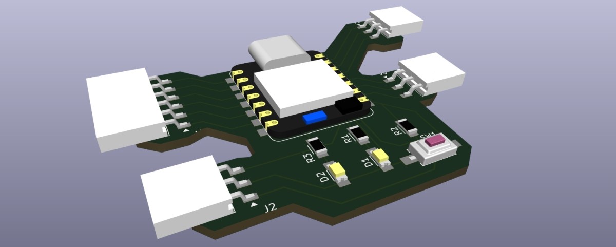
Designing a Development Board
Before starting with the design process, I looked at the FabXiao, a development board for the Xiao RP2040 by Adrián Torres. The main feature of it mainly was that relevant pins were identified and grouped with pin sockets in a reasonable way. Then, I watched Introduction and KiCad Project Creation - “Getting To Blinky” KiCad Tutorial - Part 1 by Contextual Electronics. This was a introductory video where a blinking LED circuit using the 555 timer IC was created.
Next, I installed the KiCad library for parts from the Fab Academy Inventory. I first considered to design a development board for the ATTINY412, since the XIAO already could be considered to be a development board itself. However, I decided to design a board for the XIAO ESP32-S3, since I wanted to use that for my final project. The considerations I would take now could be helpful for the creation of the PCB for my final project.
General Workflow
In the following, I describe the general workflow of how to use KiCad by just adding the ESP32-S3 and creating a PCB from that. The purpose here is to introduce the interface of KiCad.


Creating the Schematic
I considered which parts to add to the schematic. When adding the XIAO, I wanted to include pin sockets so it could be plugged in and removed easily. However, these pin sockets were not added in the PCB design itself; they were to be soldered later into the holes placed by the footprint of the ESP32-S3.
There are pins at the bottom of the XIAO (not part of the side pins). I thought about which of these pins to lead out. The MTDI, MTDO, MTCK, and MTMS pins, used for the JTAG interface, were ignored. The EN pin, which is used to enable certain functions, was also ignored. The D- and D+ pins, which are part of the USB interface, were ignored as well. One could also take D6 and D7 if necessary, as they are the same. The only pin where it seemed to be reasonable to lead it out was the the battery pin. However, I decided adding it later by soldering wire onto the backside to connect to a battery, independent of the PCB. Therefore, I only led out the pins on the sides of the XIAO.


Now the question was what else I wanted to add. Following the assignment text, we were about to add parts to be able to interact with the microcontroller. The minimum for that was a button and an LED. I also wanted to add a potentiometer, but this I thought I could just solder jumper wires on to plug it into the development board needed. In the end, I decided to add an LED which indicates if the board is powered and one that is just connected to a programmable pin.
I considered where to connect the LED — either to the 3.3V or the 5V pin. Benedikt told me that both options were fine, but it would change the required resistor. When connecting an LED to the 5V pin, a resistor value of 220 to 270Ohms was said to be a good rule of thumb. For more precision, the characteristics of the diode would need to be checked. In the design, I also used the 270Ohms resistor for the LED connected to the programmable pin. Before fabrication in one of the next weeks, I would adjust that value if necessary. When adding a resistor, there were two variants: one “1206” resistor and one “603” resistor. These numbers indicated the dimensions of the resistor’s footprint. I chose the 1206 footprint because it was easier to work with: with the 1206 resistors it is easier to fit traces between the two pads using the resistor to “jump” over them.
When adding a button, I knew I had to include a pull-up resistor. This was necessary to avoid an input pin from fluctuating between 0 and 1 when not connected to any potential. I thought about using internal pull-up resistors instead, but none of the pins provided that option, so I included it myself. Following hints from the global open time, I gave that pull-up resistor a resistance of 5kOhms.


Adding Footprints of New Parts
If one wants to add the footprint of a new part, one either has to design it on one’s own or get it from somewhere else. Possibilities to get it are to look if it is available under the Additional Files section on Digikey or to look at ultralibrarian.
Placing the Parts
After preliminarily finishing the schematic, I continued to place the parts on the PCB.


Drawing Traces
The aforementioned thin support lines help to then draw the real traces between the pads. In the PCB design rules above, I some points about what to consider when drawing the traces.


Adding the Edge Cut
In the most simple way, one could navigate to the right list of layers, select ‘Edge.Cuts’, and add a rectangle around the components.


In this design, the board is still directly on top of the PCB. It could be that one wants to add pin sockets for mounting a microcontroller already in the design. This can be done by not using the Module_XIAO-ESP32S3, but the Module_XIAO_Generic_SocketSMD component in the schematic.
Artistic PCBs
Another topic, I would like to investigate was artistic design of PCBs. For that, I wathed Artistic PCB Design and Fabrication by Emily Hammes. The speaker discussed the integration of CAD and PCB software to create aesthetically appealing and functional designs. Key design considerations included ensuring the feasibility of features like internal holes (which may be required for the aesthetics of the design), v-cuts, and mouse bites, which are useful for snapping parts of the PCB after production. Tolerances should be checked before ordering to ensure components fit correctly, considering factors such as hole sizes and the radius of tools that are used for fabrication. In particular, the speaker introduced her design workflow. It starts with roughly sketching the PCB including its basic functions and its aesthetics. Afterwards, a schematic is created (without considering the PCB’s shape). Focus thereby lies on fulfilling the PCB’s functions. The speaker then uses KiCad for component selection using KiCad, followed by CAD software for creating geometries for the edge cuts. These are then then reimported to KiCad. The final steps in the workflow include placing the components on the PCB and add traces to it. For autotracing, TopoR Lite is used in the case of curvy traces in combination with a custom script to take internal holes into account. Unique footprints for components could be incorporated into the design as artistic elements. One example could be custom-shaped soldering pads of the footprints.
In line with the idea of sustainable and creative PCB design, the Clay PCB project by Patricia J. Reis and Stefanie Wuschitz reimagined PCB production by using sustainable materials such as porcelain or clay. This approach addresses concerns related to rare earth mining and e-waste. The project was based on inclusivity, empowerment, and ethical production methods. The use of urban-mined materials, like silver, was a key part of their approach, ensuring that the production process was more environmentally friendly and socially responsible.
Reflections
What I Learned
Designing a PCB is straight forward in principle, but when it comes to details like placing and tracing, there are many things to consider. The example in this week was just a toy example. PCB design itself can be fun and you can do it even if you are not a professional circuit designer. You can fabricate PCBs for your tinkering projects just as well.
What Went Wrong
I did not understand that our task was really just to design a PCB. I thought, this week would involve electrical engineering to some extent, but it did not. This confused me and I spent much time talking to fellow students, going through the assignment requirements and discussing them, just to find out if there was more. The assignment itself, I finished in one evening. I could have been faster by just accepting that the assignment is not that much.
What Went Well
I could use this week to keep up with my other tasks (finishing earlier assignments, continuing with the final project, etc.). I finished most of the the documentation for the group assignment on thursday, after completing it.
What I Would Do Differently
Next time, if the assignment feels small, just schedule to finish it as early as possible. Then, there is more time for doing other things.
Digitial Files
- Development board: xiao_dev_board.zip (KiCad)
Use of Language Models
During writing this report, I used the following prompts asking ChatGPT 4o mini to
-
formulate prose text from bullet points:
1Take the following bullet points and form prose text out of them. Do not add any additional information. Only use those words used in the bullet points and, additionally, those that are absolutely necessary to build grammatical sentences out of the bullet points. Formulate everything in past tense. Correct spelling mistakes: 2 3<insert bullet points> -
formulate prose text from complex bullet points:
 1Take the following bullet points and form prose text out of them. Do not add any additional information. Only use those words used in the bullet points and, additionally, those that are absolutely necessary to build grammatical sentences out of the bullet points. Formulate everything in past tense. Correct spelling mistakes. Before I give you the bullet points, I would like to explain you their structure. The Bullet points are organized in the following way
 2
 3resource  1
 4- bullet point 1
 5    - bullet point 1.1
 6    - ...
 7- bullet point 2
 8- ...
 9
10resource 2
11- bullet point 1
12- bullet point 2
13- ...
14
15That means that I consulted several resources and took my notes for each. Formulate the aforementioned prose text so that it names which information came from which reference. Subdivide the text into the thematic sections "pcb design rules", "Microchip production", "reverse engineering" and "artistic pcbs":
16
17<insert bullet points>