Week 06
Electronics Design
brief.
- Utilize an EDA (electronic design automation) tool to design a development board that uses the parts from the labs inventory to interact and communicate with an embedded micro controller
a bit of context + plan for the week.
First time desiging circuit boards this week and excited about the potential for future projects! We will start this week with developing the Fab Xiao developed by fab instructor adrain torres as a starting point. Shout out adrain for providing some great documentation! If all goes well I will also like to develop a small macropad keyboard. This week we will be primarily be using KiCad to design our board.
As always lets begin with some terminology. Its helpful to understand a baseline of electronic compoinents which we will build off from embedded programing week.Working knowledge of these components is important so we know what kind of parts are available to use and place on our board.
helpful hints and resources.
weekly terminology:
Overview of components
EDA: Electronic design aoutomation. KiCad and Eagle are examples
resistor: limits current flow, usually denoted by units of ohms. I = V/R where I is current. Analogy - flow of water in a pipe, voltage is push, resistance is the nozzle.
capacitor: can store and release electrical charge quickly. Also to filter unwanted noise from signals C=Q/V C is how much charge your store vs how much voltage there is. think of filling up a reservoir
diode: used to allow current to only flow in one direction
crystal: used as a time keeper in electronics and microcontrollers
inductor: oposites of capacitors, they store energy in a magnetic field, used as filters to pass lofrequencies
transistor: 2 types, will mostly use mosfit transistors. almost like a variable resistor with gates that control resistors.
voltage regulator: used to set a fixed voltage level commonly used to step down voltage for specific componets.
analog pins:
digital pins:
ground: in miocrocontrollers its used as a reference point for all voltages. considered to be "0" volts.
power: source of electrical energy in your circuit.
UART protocal: Universal asyncronous reciever/transmitter, serial communication protocal used to communicate between two devices
SPI protocal: Serial peripheral interface, used to communicate between microcontrollers and other devices. high speed and minumum 3 pins
KiCad Terms
symbol library: collection of schematic symbols that represent electronic components. contains graphical representation of the component along with their properties and pin definitions. used tin the schematic editor to create the schematic of the circuit.
footprint library: collection of pcb footprints that represent the physical layout of the component. contains the physical dimensions of the component and the location of the pads. used in the pcb editor to create the layout of the pcb.
trace: conductive path on the pcb that connects two or more pads. used to connect components together.
resources to get started:
Pull up Vs Pulldown resistors explained
KiCad Download
Sparkfun's beginners guide to KiCad
Fab-Xiao docs! dev board by Adrian Torres
FabAcademy Kicad Library
Huge DigiKey Kicad Library
Kicad Tutorial based around mechanical keyboards!
Deep dive into electronics theory/componets/design
Pipeline
General pipline for workflow in KiCad is as follows:
- Download KiCad
- Download and set up compnent libraries. Only needs to happen once, and you can use for future projects
- Start w/ file new project
- Draw schematics- We start in the schematic environment firts. Utilizing componet symbols we draw lines/associations between our parts. Think of this as the road map/pre-planning stage of the pcb. doing this well will help make pcb trace easier.
- Design PCB- We then move to the PCB environment. This is where we actually design/develop our PCB, place componets, plot traces, add via's or through holes, edgecuts.
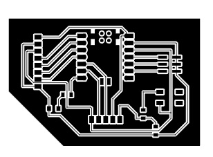
- Package files- export necessary files for production ex. svg traces, gerber files, BOM
Developing Boards in KiCad
I followed this Kicad tutorial closely. It goes from library setup --> schematic creation-- > and PCB tracing. Really well done and definetly recomend it!
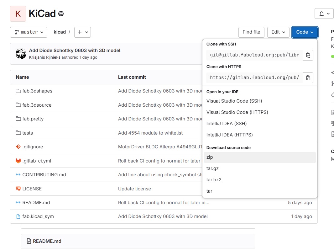
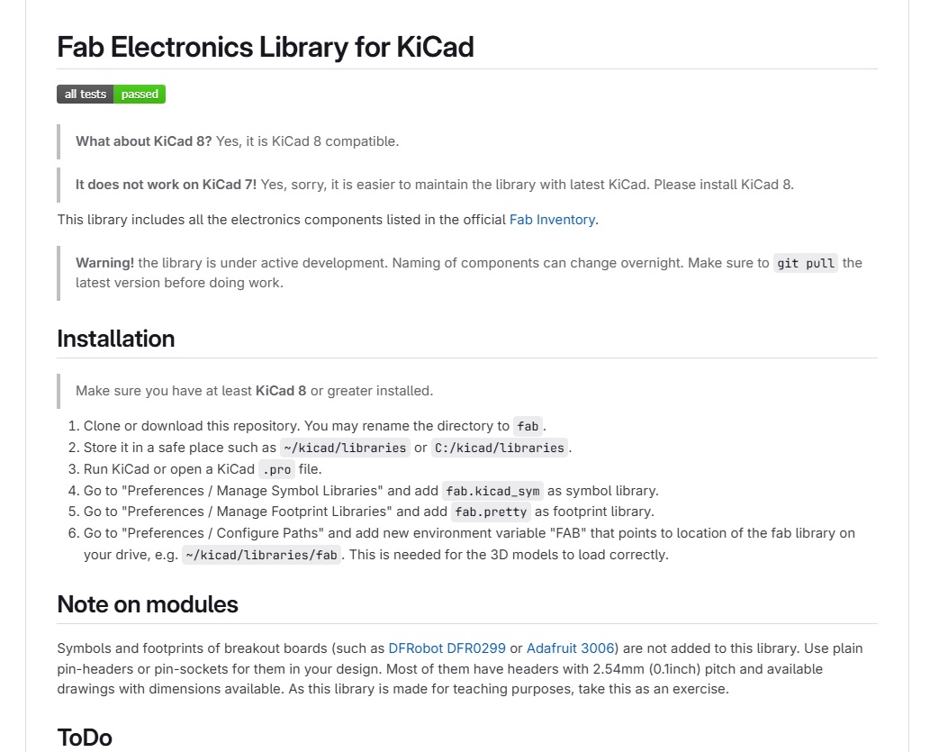
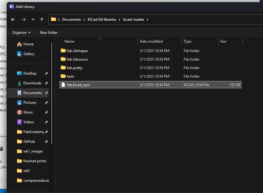
First step is to download KiCad. I downloaded the latest version from the KiCad website. I then downloaded the fabacademy library and the digikey library. The fabacademy library is a great resource for the components we will be using in the lab.
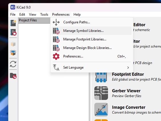
We then configure our symbols and footprints. The symbols are annotations of the components and are used when we draw our schematic. The footprints are just that and denote the size and placement of the solder pads. The foot prints are used when we plot our PCB. The Fabacademy KiCad library is a great start and also has instructions to configure.
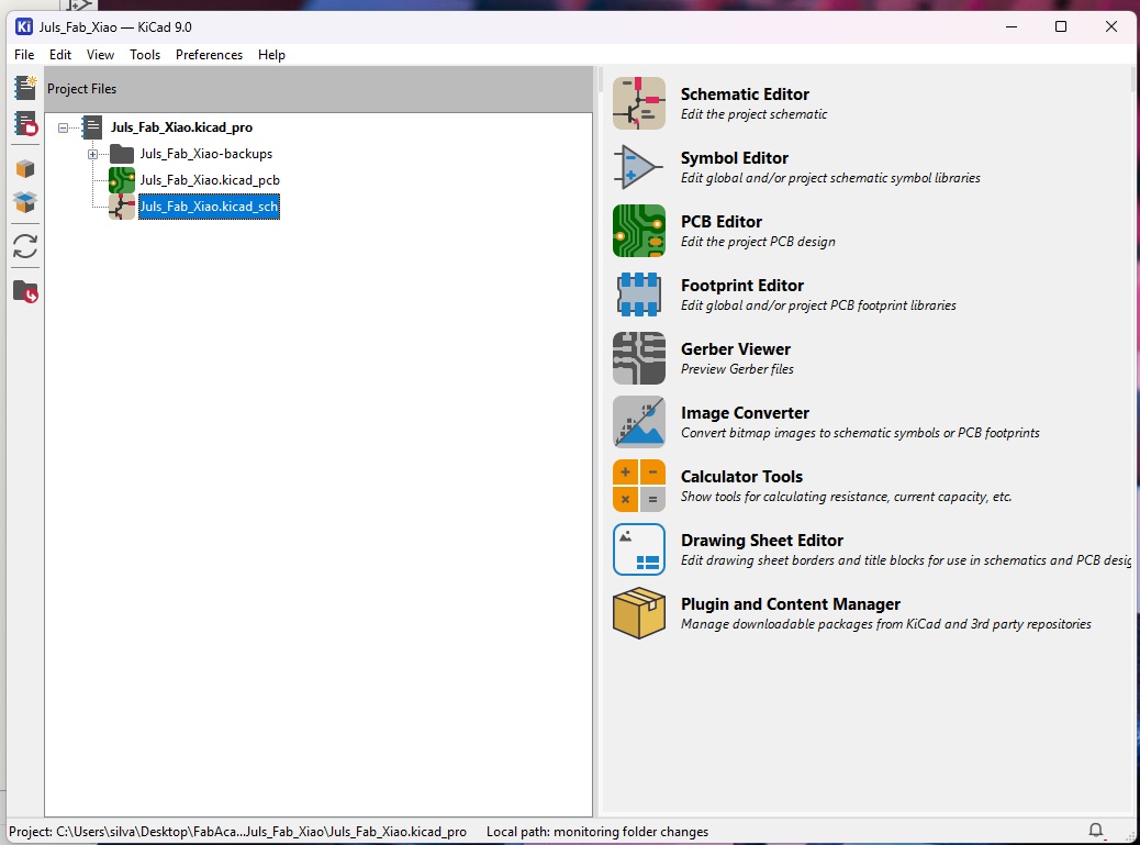

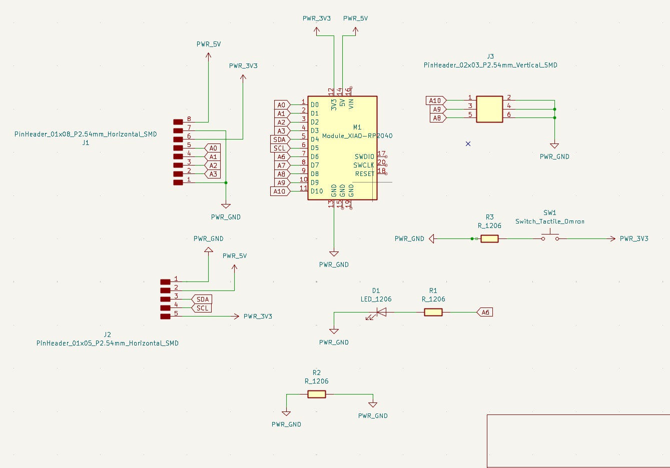
After opening up a new project we begin by plotting a schematic, essentially drawing lines and making connections between the componts we will be using. Its important to note that this is just establishing the relationship between compnents not actually drawing out our pcb traces ( we will do that in the next step in the PCB environment). The schematic will create the rats nest that we will then "untangle" later. Think of the schematic as the map or legend.
Using the Fab Xia as referecne I began placing symbols and draeing the scematic. I found it helpfult to have the pinout of the microcontroller pulled up as I was drawing. We can use hot key "A" to bring up the symbol library. Search for the part that you want and place the component in the schematic.
utilizying the tool bar on the right we can usethe line tool to connect componets. I also utilized the Global labels to associate different pins.
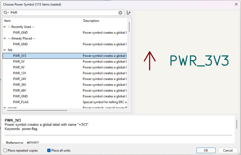
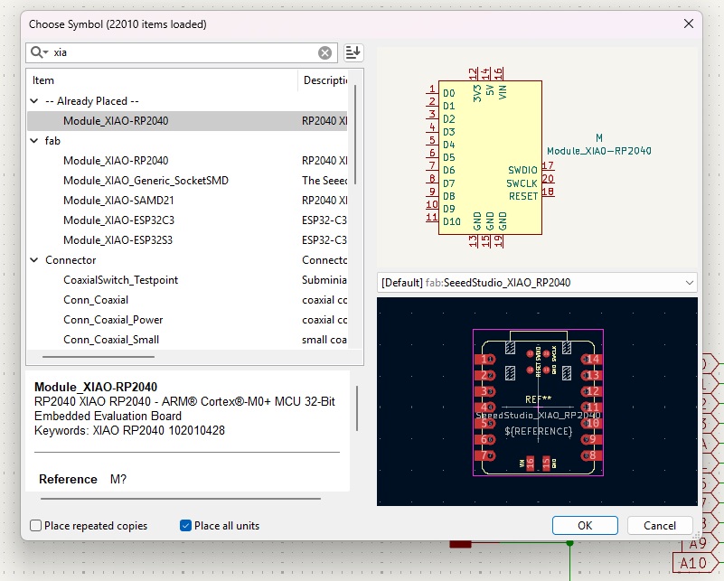
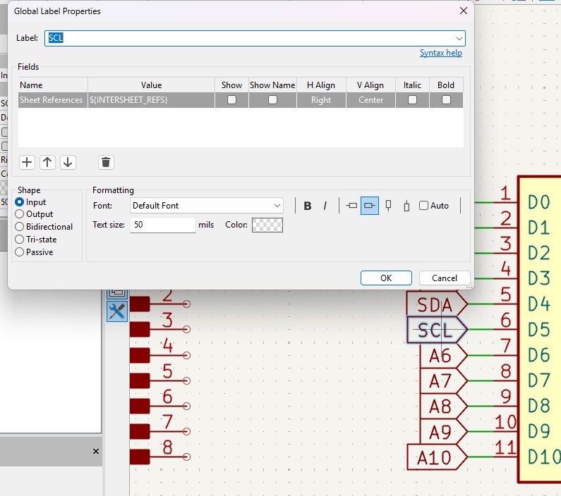
Thi Finished schematic looked like this:
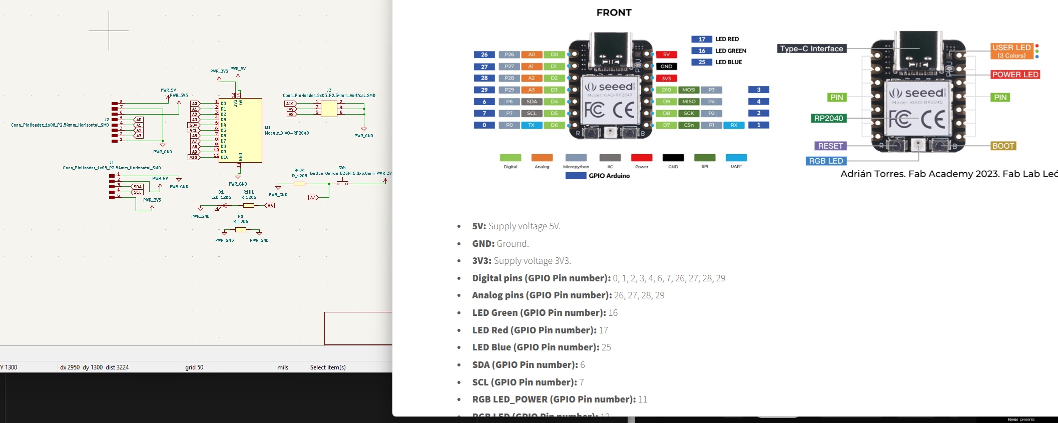

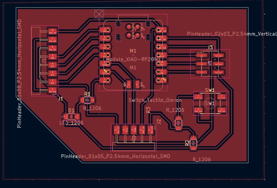
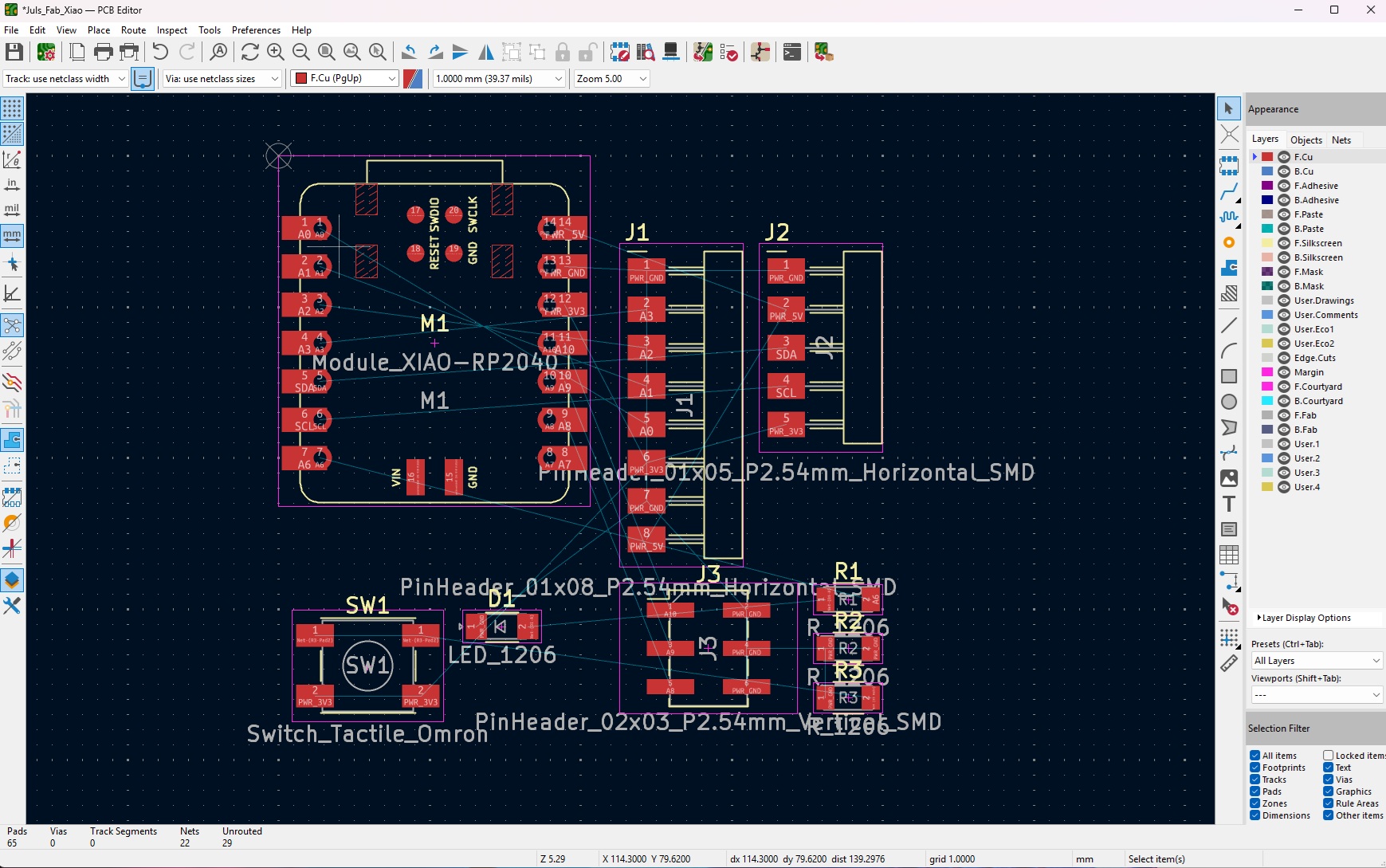
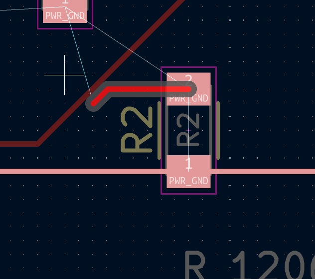
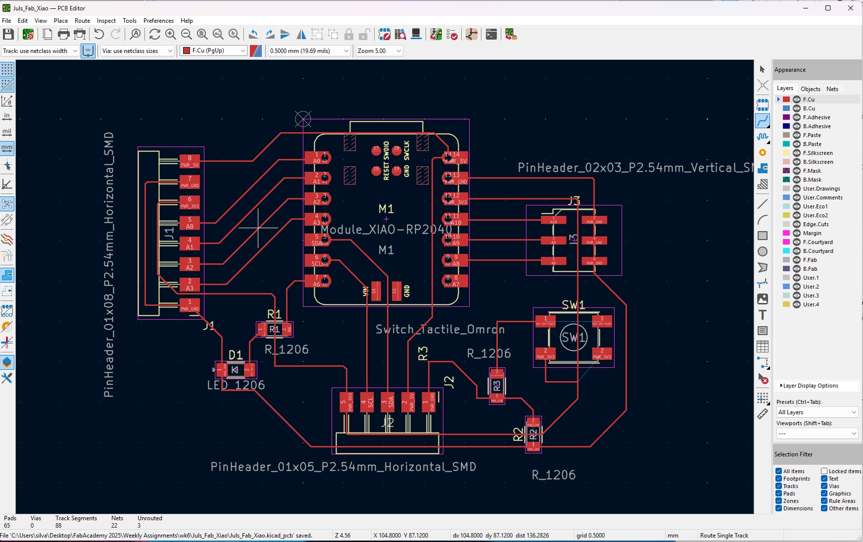
After finishing the schematic we can then move to the PCB environment. This is where we will actually design our board and plot out traces. We navigate to the top tool panel and click the pcb environment. Here we can place our rats nest and begin untangling our componets. I referenced Adrains documentation and used the route track tool "x" to begin drawing traces to component pins/terminals. Here its important to plan your traces so you dont have overlaping traces. KiCad will let you know if you have a trace error and try to reroute you.
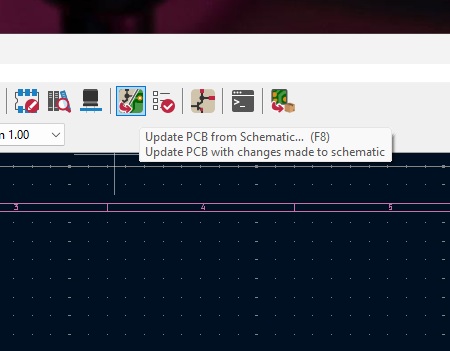
If you accidentally delete an item or add componts to your scematic you can always use the "update pcb" button to update your workspace. Yayy for paramatrics
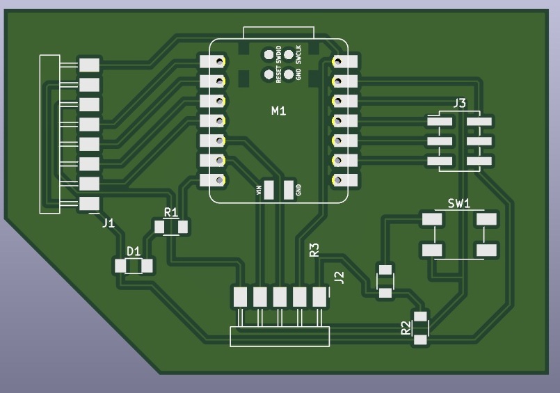
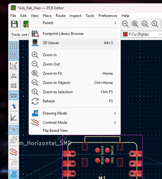
We can also navifate to the 3d viewer to see a realtime 3d model of the pcb.
The Finished schematic looked like this:


conclusion
KiCad is extremly powerful. Having the abilty to desgin your oen custom PCB'c unlock a hole new level of whats possible in the lab.
- KiCad is powerful, but adding custom libraries like the fabacademy's and digikeys makes it worth its while.
- Excited to machine the board next!
- Its great that we can export a .stl of the pcb so we can build an enclosure around it.
- I need to dive deeper into electronics concepts and components.
files
Click the link below to try for yourself:
Download the KiCad project filesProduction files
Edge Cuts
Front Copper