Electronics Design
This week, I got the opportunity to experience electronics design. For our group assignment, I contributed to testing our lab equipment to observe the operation of a microcontroller circuit board. We used oscilloscope to test the operation of our circuit that consisted of an LED connected to a Raspberry Pi Pico. Then, we used a multimeter to measure the voltage, resistance, and current values of this same circuit.
You can see our group assignment with this link
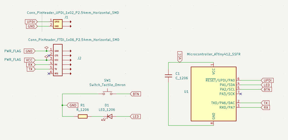
I didn't have any prior experience with electronics before Fab Academy. Therefore, for my individual assignment, I first learned how to use KiCAD from a video by Krisjanis Rijnieks suggested by my local instructor Sedat. While watching this video, I designed the same circuit on my own KiCAD. This circuit consists of ATtiny as a microcontroller, a switch, an LED, and a resistor. It also includes pinheaders. Below is the schematic of my design.
I also downloaded the KiCAD library by Krisjanis Rijnieks and used it in my designs. Now I will briefly talk about what I learned related to KiCAD as I went through Kris's video.
KiCAD Schematic Basics
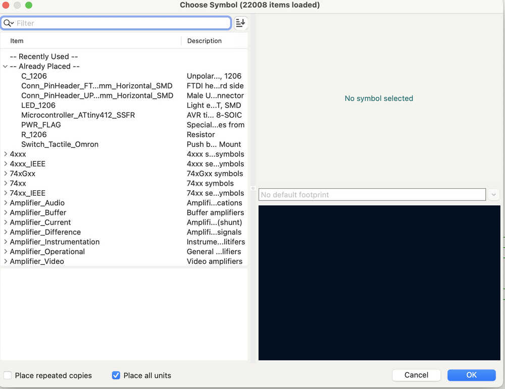
Click on "A" to choose a symbol from the libraries you have.
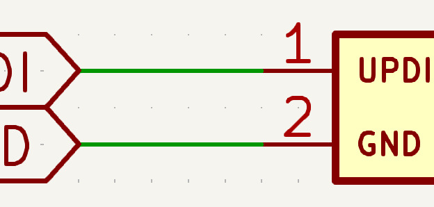
Draw wires by clicking on "w" which will allow you to engrave paths for the electricity to go through on your PCB.
You shoul place no connect flags by clicking on "Q" if your port is not connected to anywhere.

In your schematic, it is hard to connect everything via cables. Therefore, place global labels to connect ports of your components without using any cables. You'll of course need actual tracks when you are designing your PCB. The following images illustrate how I connected my ATtiny with my Pin Header.


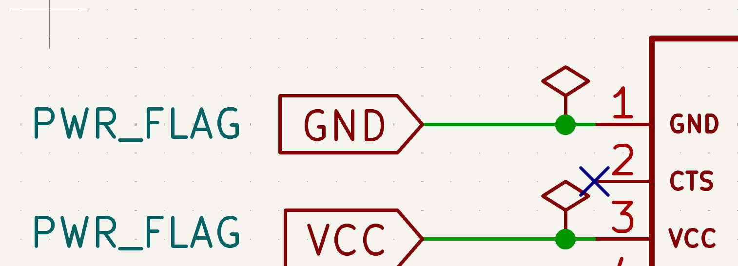
KiCAD doesn't know where the power comes and where it exits. Therefore, it is important to add power flags to indicate these.
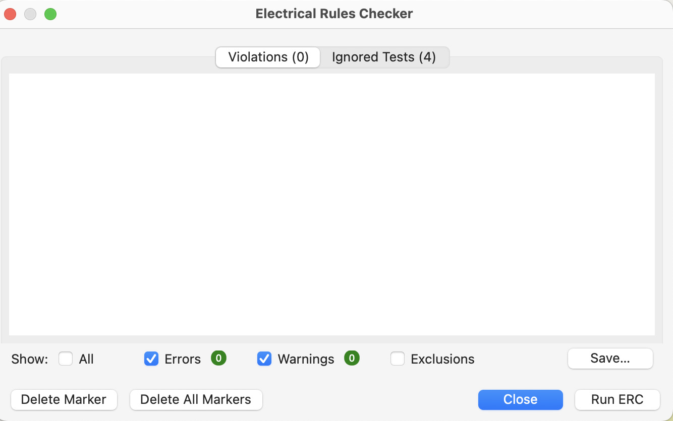
After finalizing everything, click on Electrical Rules Checker (ERC) and then "run ERC" to see if your schematic has any errors. Correct your schematic errors until you see the following screen.
KiCAD PCB Editor Basics
Click on the Route Single Track icon to connect the routes that you have designed on the schematic. Click on "D" to adjust the routes. The corners should be 45 degrees.

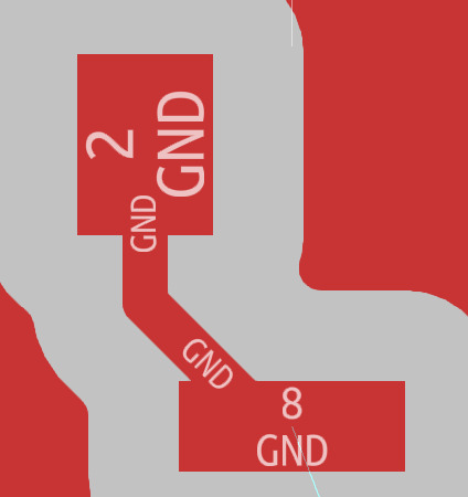
All the ground should be connected to the whole ground circumferencing the board. In my design, only the grounds of the ATtiny and the capacitor are connected to each other. The others are connected to the big ground.
In order to make this big ground, click on the "Draw Filled Zones" icon, and then select the whole region where you want your ground to include. Your copper zone properties should be the following.
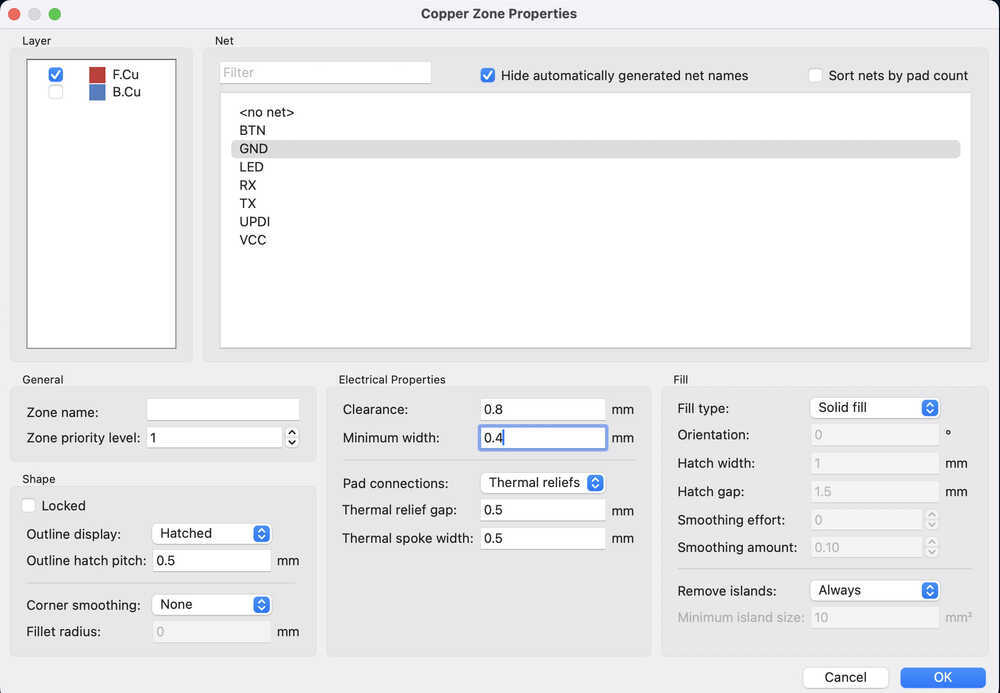
Then, click on "B" to fill the whole zone. If you want to change the grid size, the size between the two dots on your design, click on the grid at the top.
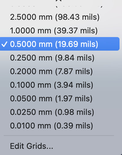
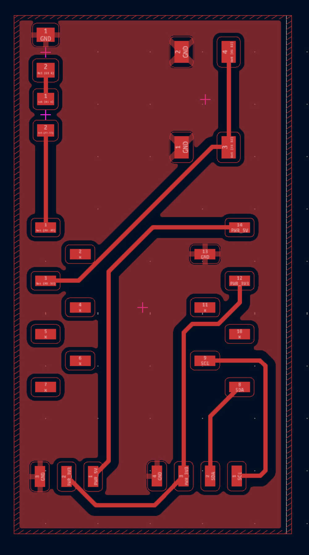
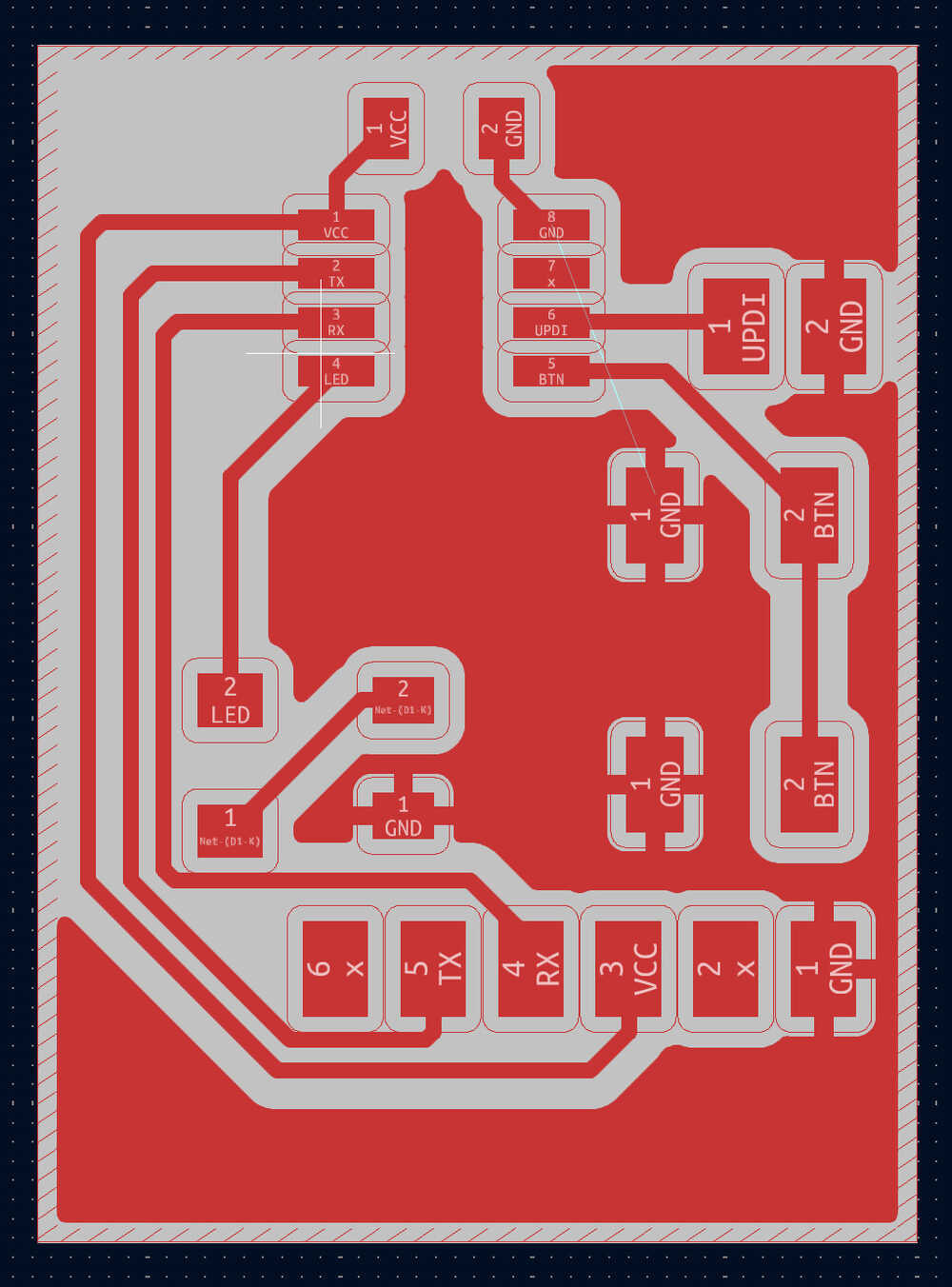
Do all these preceding steps when F.cu is selected on the right. This means you are using cupper to proceed these steps. "F" indicates that this is the front layer of your PCB. If you want to make a two-sided PCB, then you should also use the B.cu layer. Then, select Edge.Cuts to make your actual board. Click the eye icon on the layers that you do not need to close them. My final design looks like the following image.
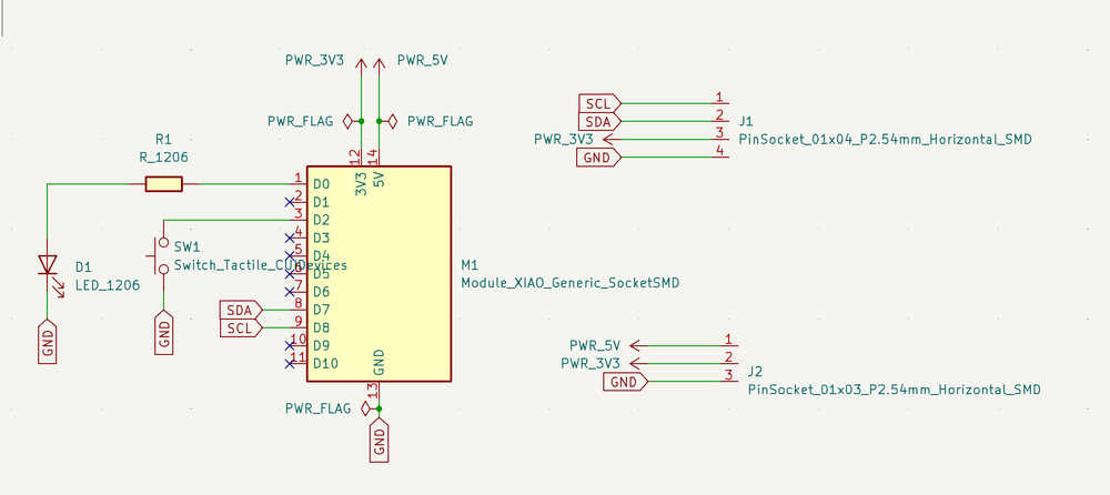
After learning how to use KiCAD, I designed my own simple board. In this process, I benefitted from another Fab Academy student Dora's board on her Electronics Design Assignment page. My schematic design is the following.
My initial board design was the following.
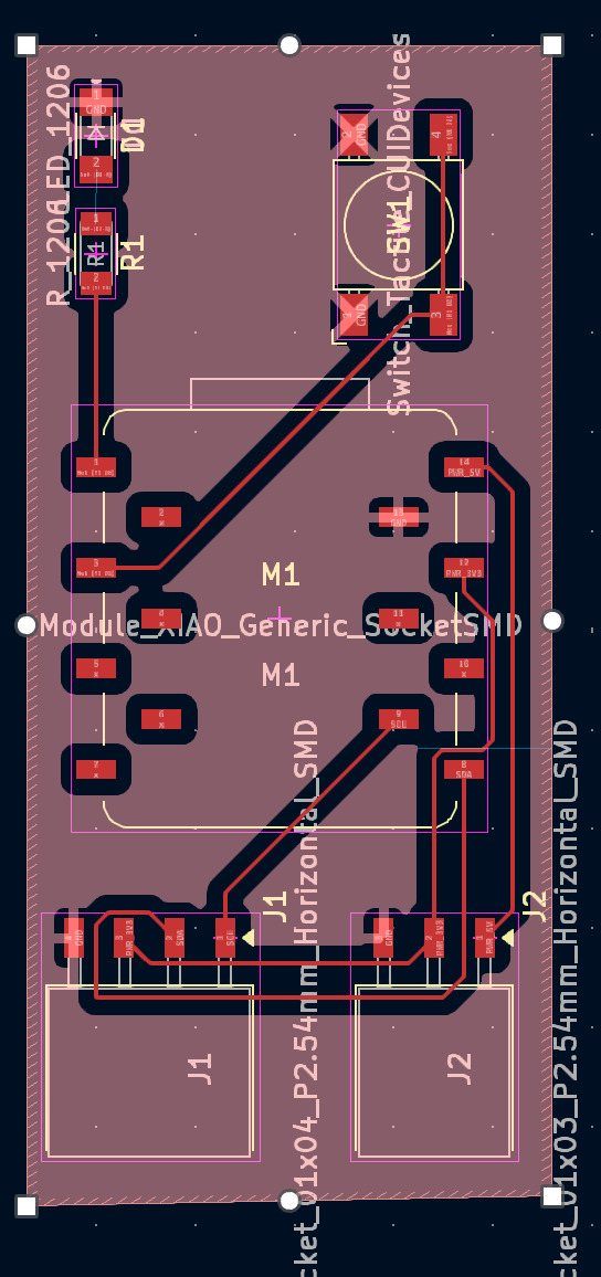
However, I realized that not all grounds were connected.
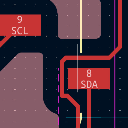
Therefore, I changed the places of my two socket headers. My final design looks like the following image.
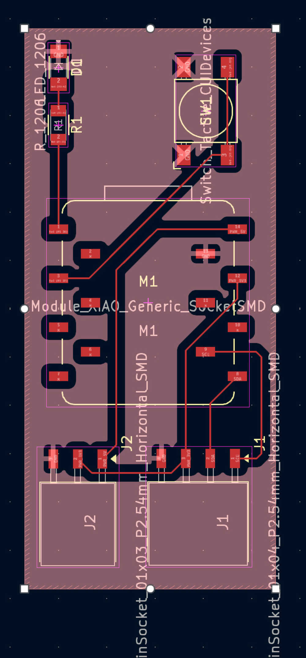
Solving the Issues
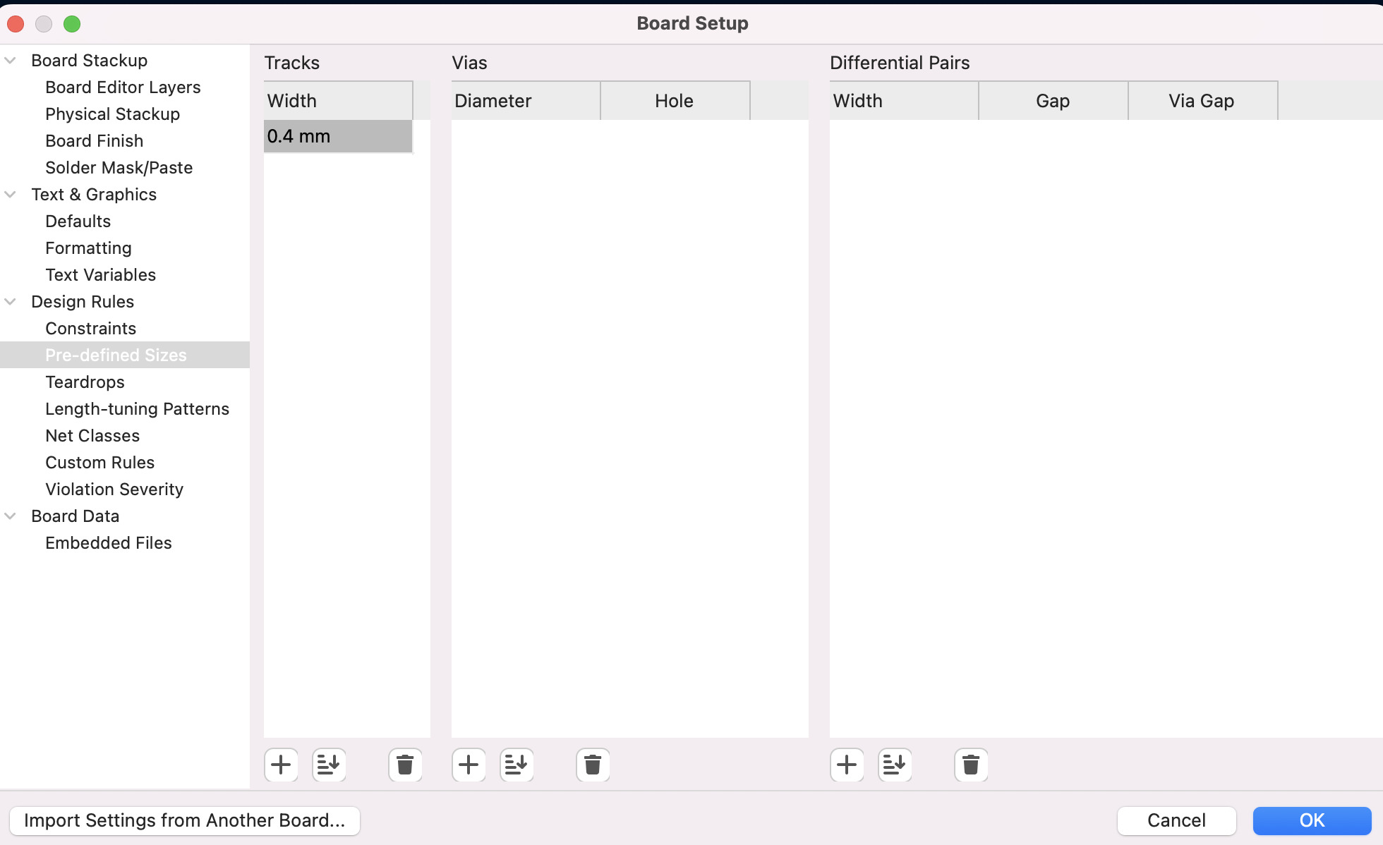
After showing my design to Krisjanis Rijnieks, he told me that my tracks were too thin. Therefore, I changed the thickness of my tracks to 0.4 mm from 0.2 mm using the Board Setup menu's Pre-defined Sizes.
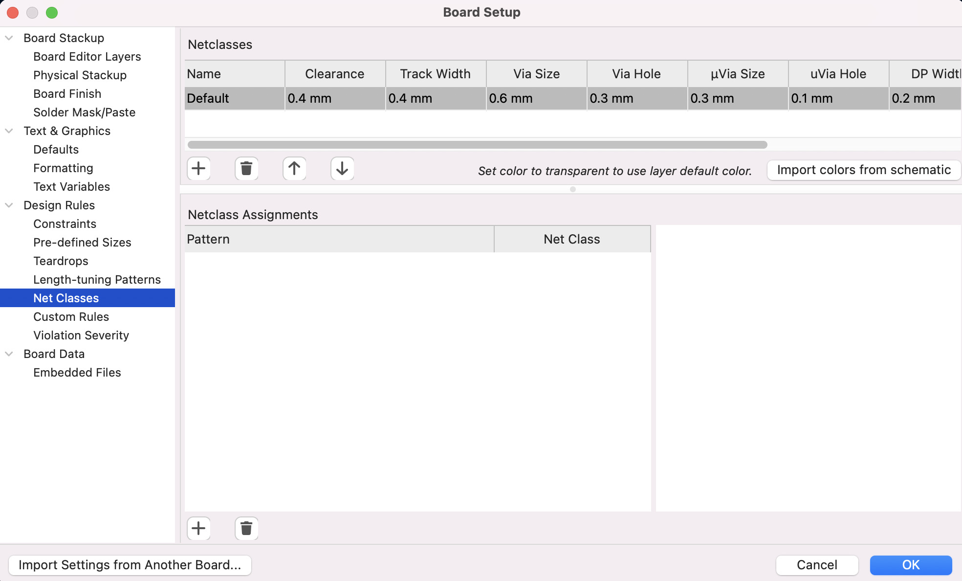
I also changed the clearence and track width to 0.4 mm on Board Setup menu's Net Classes.
My tracks are now thicker, and my design is complete.
