Week 8: Electronics Production
Group Assignment
Click to access the group assignment
This week, I learned how to produce a custom PCB using a CNC milling machine. The process included file preparation, toolpath generation, probing, milling, and component soldering.
I started by importing my Gerber files into Cube 3D CAM Pro. This software allowed me to visualize the PCB design and generate G-code for the engraving and cutting operations.
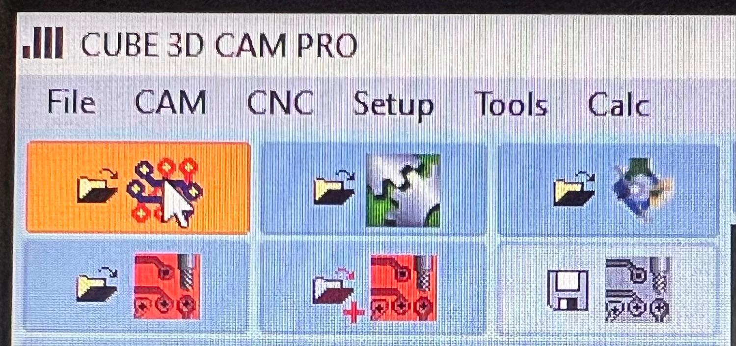
After importing the Gerber files, I previewed the traces and outline. This helped me confirm the alignment, scaling, and overall board layout.
Generating Toolpaths in Cube 3D CAM Pro
Before milling, I generated toolpaths for both engraving and cutting in Cube 3D CAM Pro:
- Engraving: I selected the “Top Copper” layer and used a V90 engraving bit with ~0.1mm depth to isolate copper traces.
- Cutting: For the outline, I switched to a 1.0mm flat end mill and set the depth to ~1.8mm using multiple passes.
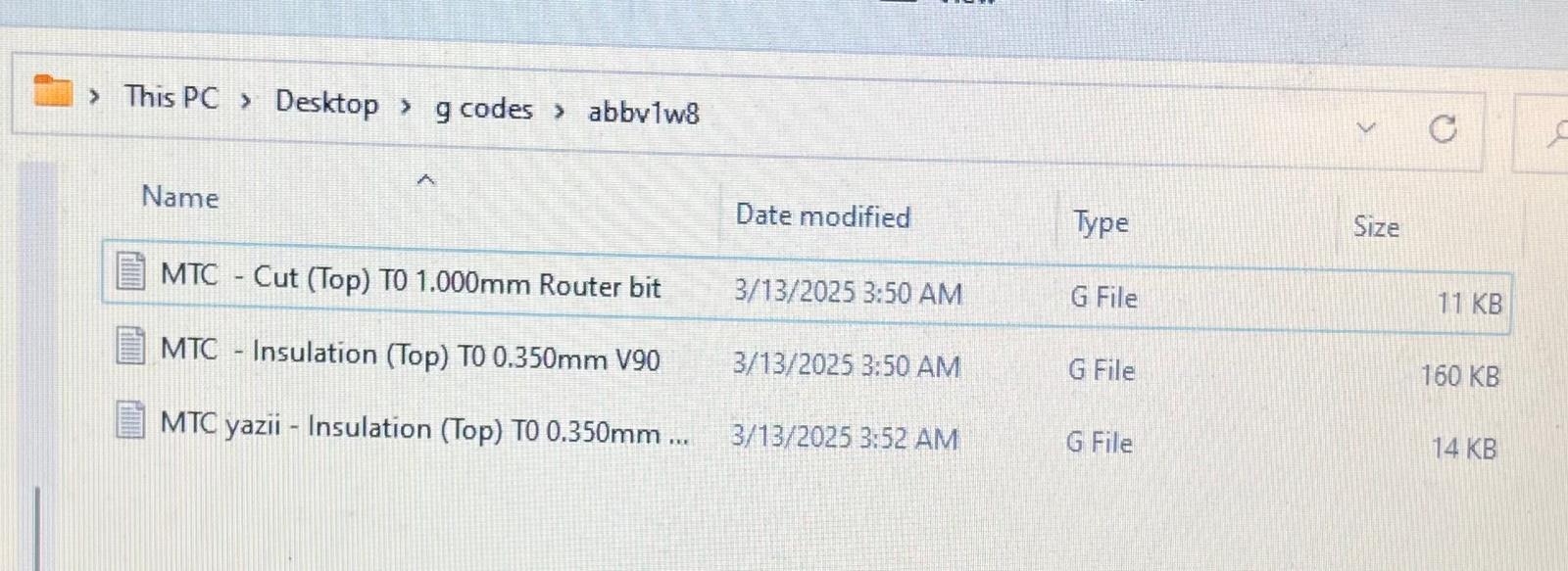
These are the G-code files used for the milling process — one for engraving with the V90 bit, and one for cutting with the 1.0mm bit.
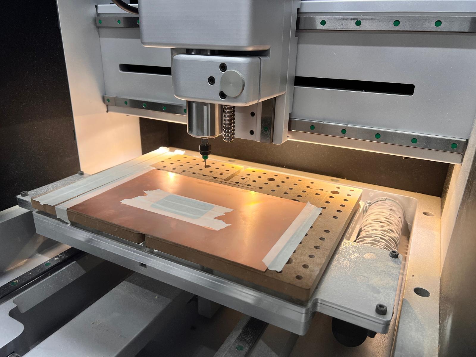
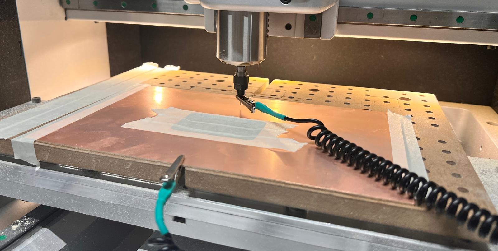
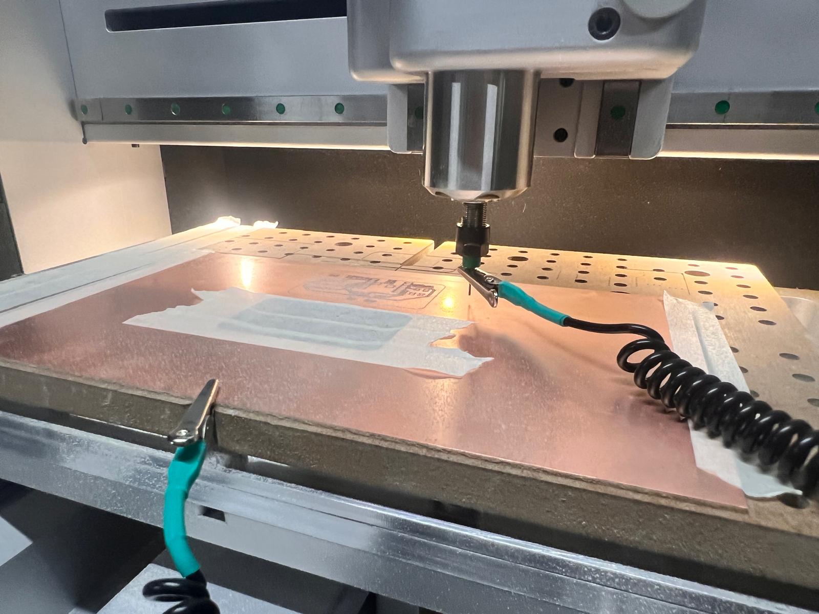
I attached the copper-clad board securely onto the sacrificial layer with tape to prevent any movement during milling.
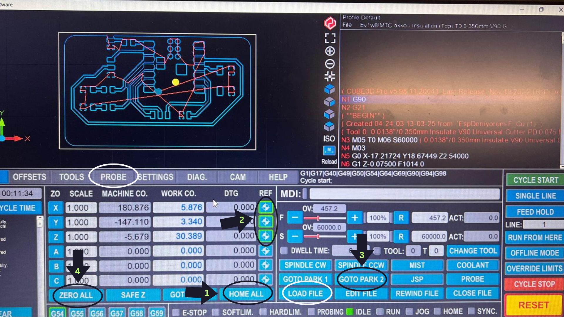
Once the board was fixed, I turned on the CNC machine and opened the machine control interface.
Machine Setup Sequence:
1. Click HOME ALL – this moves the machine to its default reference position.
2. Wait until all three status indicators turn green — this confirms homing is complete.
3. Click GOTO PARK 2 to move the toolhead to the parking location.
4. Click ZERO ALL to reset the X, Y, and Z work offsets.
After this sequence, I changed the bit and began probing.
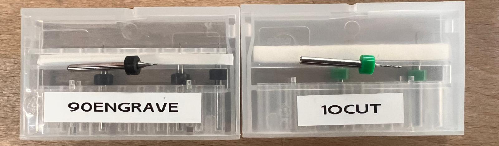
Here are the tools used:
- V90 Engraving Bit for isolating traces
- 1.0mm End Mill for cutting out the board
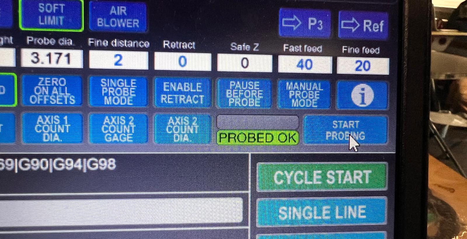
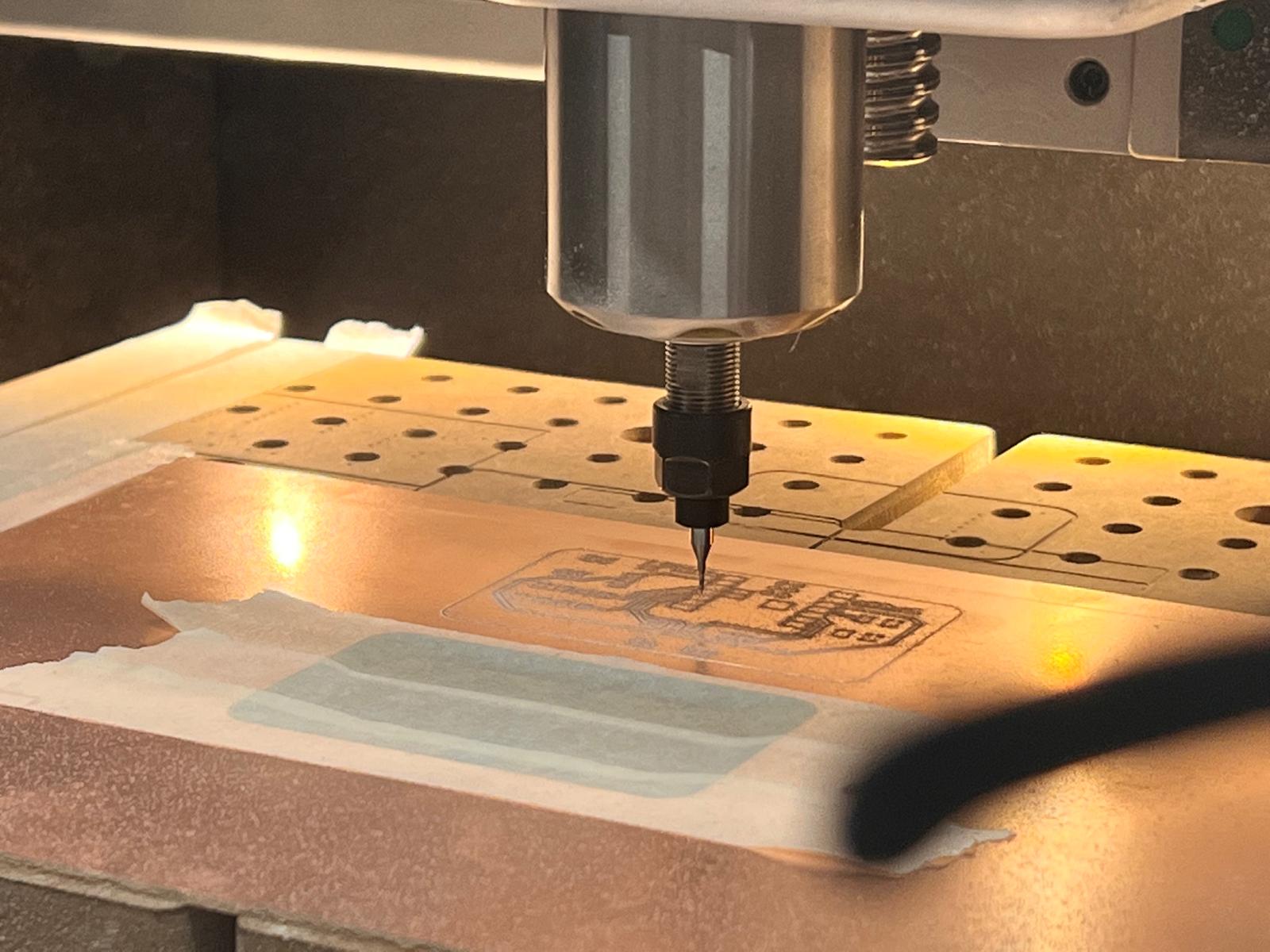
I performed surface probing using the attached probe cable. The system measured the Z-surface offset to compensate for any unevenness across the copper board.
Using a V90 engraving bit, I started the engraving operation to isolate the PCB traces. The machine followed the G-code path precisely.
After changing the tool to a 1.0mm flat end mill, I probed again to account for the new tool length. This ensured that the cutting depth would be accurate.
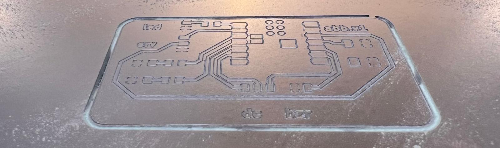
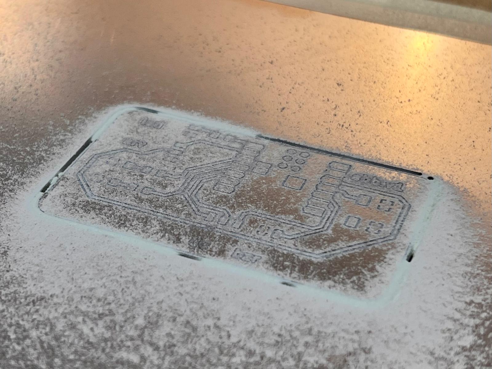
The board is now fully milled. Both the traces and the board outline have been cut, and the PCB is ready for assembly.
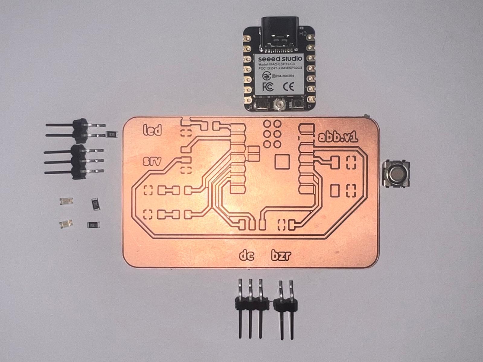
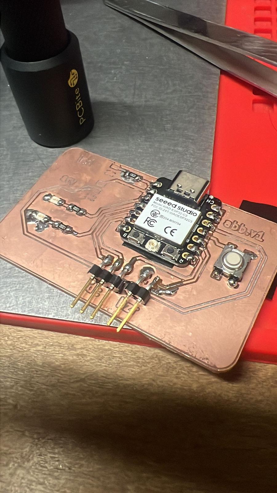
This is the cleaned PCB with visible pads and silkscreen text. It’s designed to support an ESP32-C3 microcontroller, LEDs, headers, and a button.
This was my first soldering attempt. Some connections were cold or excessive, causing unreliable behavior in the board.
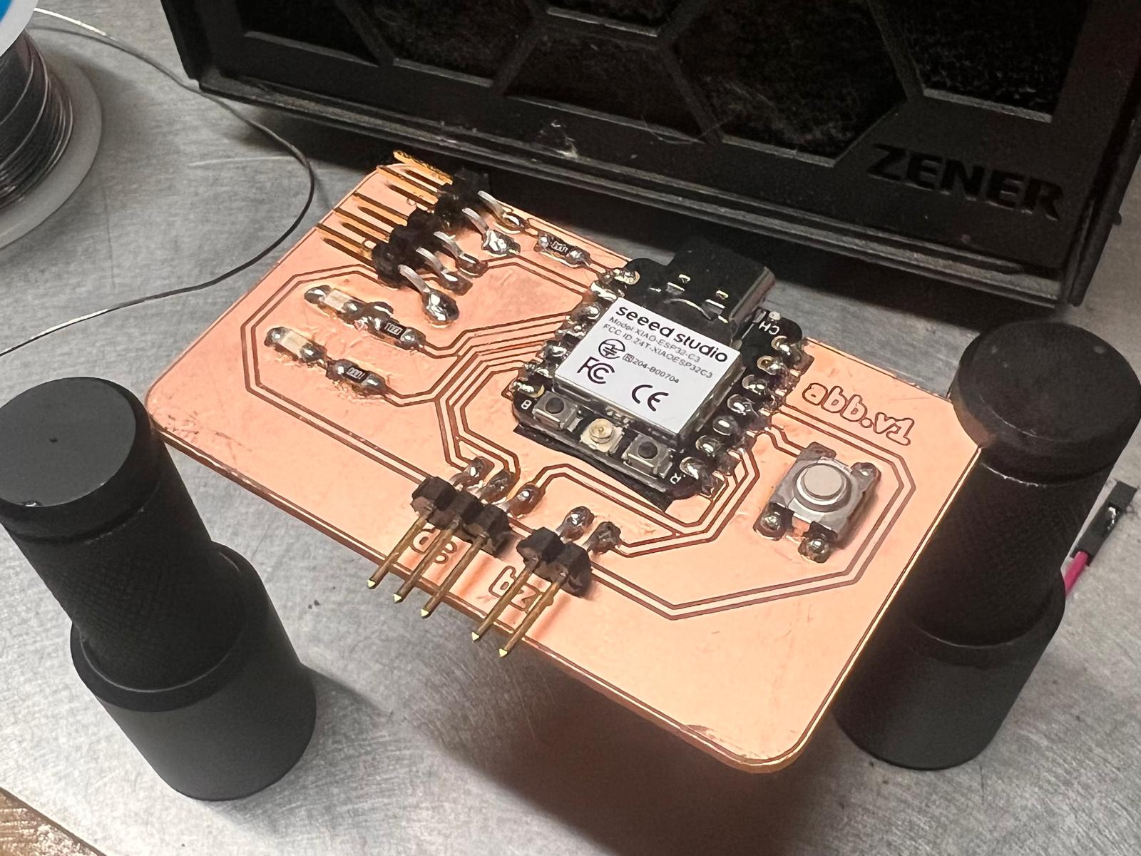
After reworking the joints, I managed to achieve clean and reliable soldering. The board is now fully functional.
Testing the Board Functionality
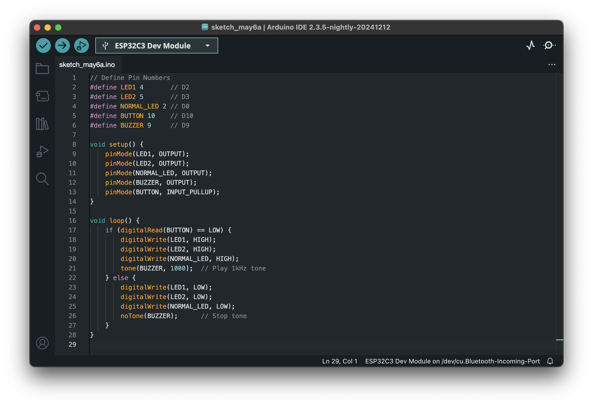
To test the board I designed and milled, I used the Arduino IDE to upload a simple sketch. The goal was to check whether both SMD LEDs and the buzzer responded correctly when the button was pressed.
Code Explanation
I wrote a program that:
- Configures the LEDs and buzzer as output devices.
- Uses the internal pull-up resistor on the button pin.
- Activates both LEDs and the buzzer when the button is pressed.
- Deactivates everything when the button is released.
// Define Pin Numbers
#define LED1 4       // D2
#define LED2 5       // D3
#define BUTTON 10    // D10
#define BUZZER 9     // D9

void setup() {
    pinMode(LED1, OUTPUT);
    pinMode(LED2, OUTPUT);
    pinMode(BUZZER, OUTPUT);
    pinMode(BUTTON, INPUT_PULLUP);
}

void loop() {
    if (digitalRead(BUTTON) == LOW) {
        digitalWrite(LED1, HIGH);
        digitalWrite(LED2, HIGH);
        tone(BUZZER, 1000);  // Play 1kHz tone
    } else {
        digitalWrite(LED1, LOW);
        digitalWrite(LED2, LOW);
        noTone(BUZZER);      // Stop tone
    }
}
How It Works
- When the button is pressed, both LEDs light up and the buzzer emits a 1000 Hz tone.
- When the button is released, everything turns off.
What I Confirmed
- LED1 and LED2 (SMD) light up correctly.
- Buzzer produces sound when triggered.
- Button is properly debounced and responsive thanks to internal pull-up.
Final video:
Hero Shot