Week 6: Electronics Design
Goal of the Week
This week’s assignment was to design a pcb(printed circuit board). and perform all necessary checks for fabrication. I decided use the Seeed Studio XIAO ESP32-C3 and design a custom board that includes:
- 2 mini LEDs
- 1 normal LED
- 1 button
- 1 buzzer
- 1 DC motor
- 1 servo motor
Group Assignment
Click to access the group assignment
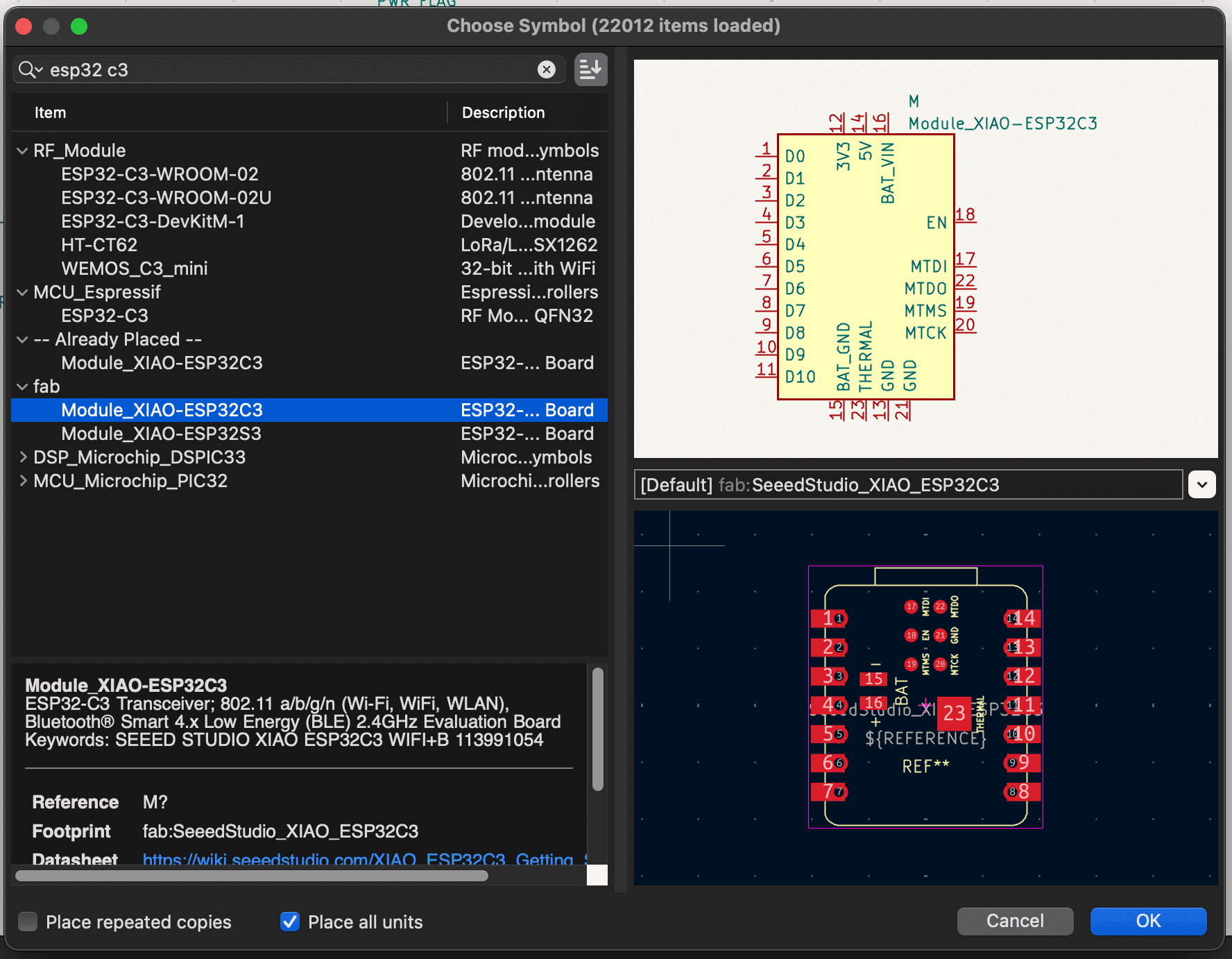
Step 1: Selecting the ESP32-C3 Symbol
I selected the correct microcontroller symbol from the KiCad libraries. I chose Module_XIAO-ESP32C3 from the fab library, which matches the Seeed Studio XIAO ESP32-C3 module.
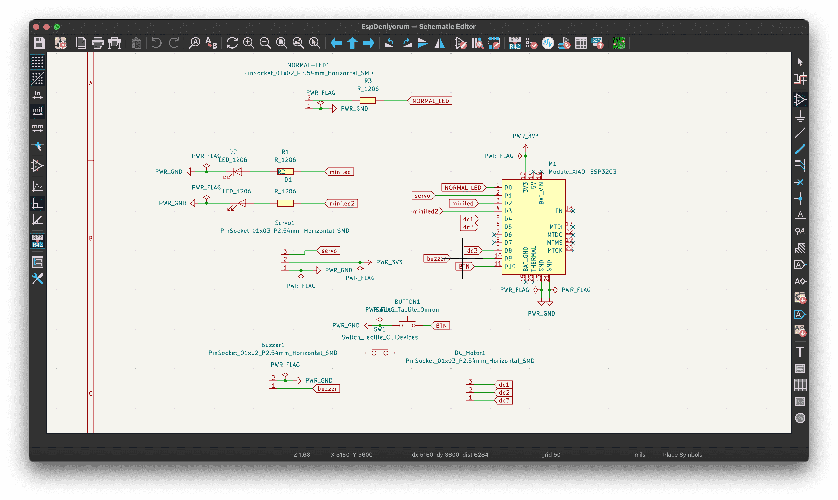
Step 2: Schematic Design
I designed the schematic using the KiCad Schematic Editor. I began by placing the ESP32-C3 module from the fab library and added the supporting components: two mini LEDs, one normal LED, one tactile button, a buzzer, a servo motor header, and a DC motor header.
Each component was connected to an appropriate GPIO pin of the ESP32-C3. I used PWR_FLAG symbols on both the 3.3V and GND lines to avoid power connection errors during ERC.
All non-polarized components were labeled, and I kept wiring clean by using Label (L) and Net (N) tools to avoid tangled wires.
Useful Shortcuts in Schematic Editor:
A– Add a new componentW– Draw a wire (connect pins)L– Add a labelR– Rotate selected itemCtrl + E– Edit component propertiesShift + Click– Highlight connected netAlt + G– Group select multiple elements
Step 3: Electrical Rules Check (ERC)
- ⚠️ Initial warnings about unconnected power pins were resolved by adding power flags.
- ✅ Final result: No remaining warnings or errors.
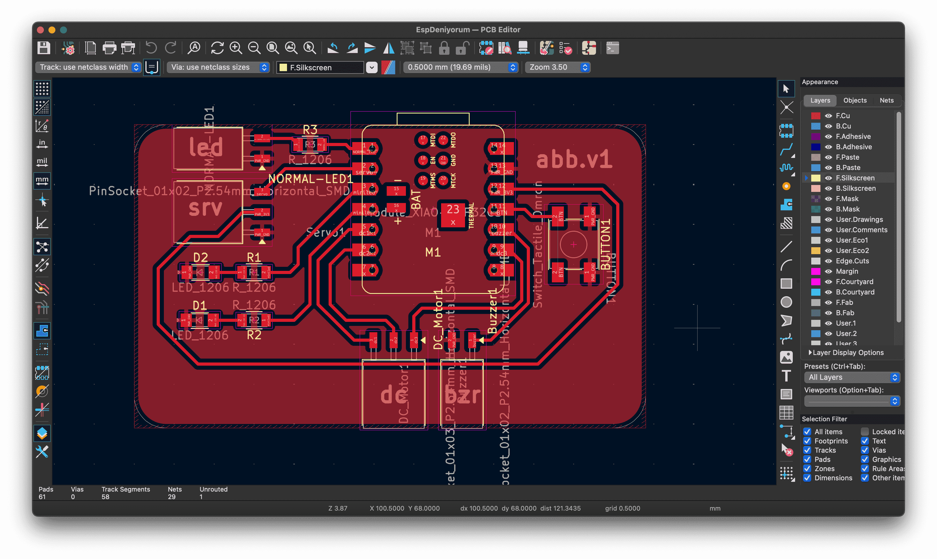
Step 4: PCB Layout
Once the schematic was complete and error-free, I assigned footprints and switched to the PCB Editor. I started by arranging the components logically — placing the ESP32-C3 in the center and distributing headers, LEDs, and resistors around the board edges for easy access and neat routing.
I used a 0.4 mm track width for signals and added a ground fill zone on the front copper layer (F.Cu) using the zone tool (Shift + Z). All signal traces were routed manually for better control using the interactive router.
I also added labels for clarity and testability. Components are spaced to avoid soldering issues, and I used the DRC tool frequently during layout to make sure all clearances and trace widths were correct.
Useful Shortcuts in PCB Editor:
Ctrl + Shift + R– Update PCB from schematicAlt + 3– 3D View of PCBX/Y– Start a horizontal/vertical trackM– Move selected componentR– Rotate componentShift + Z– Add filled zone (for ground planes)Ctrl + H– Highlight netDelete– Remove track or zone
Step 5: Design Rules Check (DRC)
- ✅ All tracks met clearance and width requirements.
- ✅ Ground zone filled properly.
- ✅ Result: 0 errors, 0 warnings.
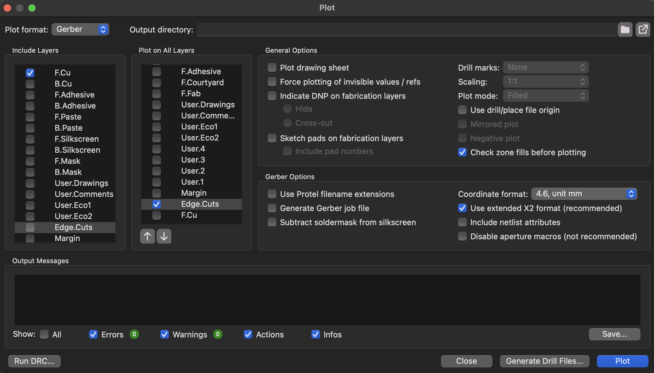
Step 6: Generating Gerber Files
Using the Plot window, I exported the Gerber files needed for PCB manufacturing. I enabled:
- F.Cu, Edge.Cuts
- "Check zone fills before plotting"
- X2 coordinate format
Final Pin Mapping Table
| Component | ESP32-C3 Pin | Board Label |
|---|---|---|
| LED1 (Mini) | GPIO4 | D2 |
| LED2 (Mini) | GPIO5 | D3 |
| Normal LED | GPIO2 | D0 |
| Button | GPIO10 | D10 |
| Servo Motor (PWM) | GPIO3 | D1 |
| Buzzer (PWM) | GPIO9 | D9 |
| DC Motor Speed (PWM) | GPIO6 | D4 |
| DC Motor Direction 1 | GPIO7 | D5 |
| DC Motor Direction 2 | GPIO8 | D8 |

Download Design Files
Here is the Edge_Cuts
Here is the F_Cu
What I Learned
This week taught me:
- How to use custom microcontroller modules in KiCad
- How to assign pins with a balance of hardware constraints and software usability
- How to route multi-component boards cleanly
- How to validate a design through ERC, DRC, and generate professional-grade Gerber files