
W8 | Electronics Production
📝 Group Assignment:
- Characterize the design rules for your in-house PCB production process: document the settings for your machine.
- Document the workflow for sending a PCB to a boardhouse.
- Document your work to the group work page and reflect on your individual page what you learned.
What We Did
For this group assignment, we characterized the in-house PCB production process at our lab using the Carvera CNC milling machine. The goal was to document all the settings and steps needed to go from a PCB design to a physical board, and to determine the minimum trace width that the machine can produce reliably.
The Machine
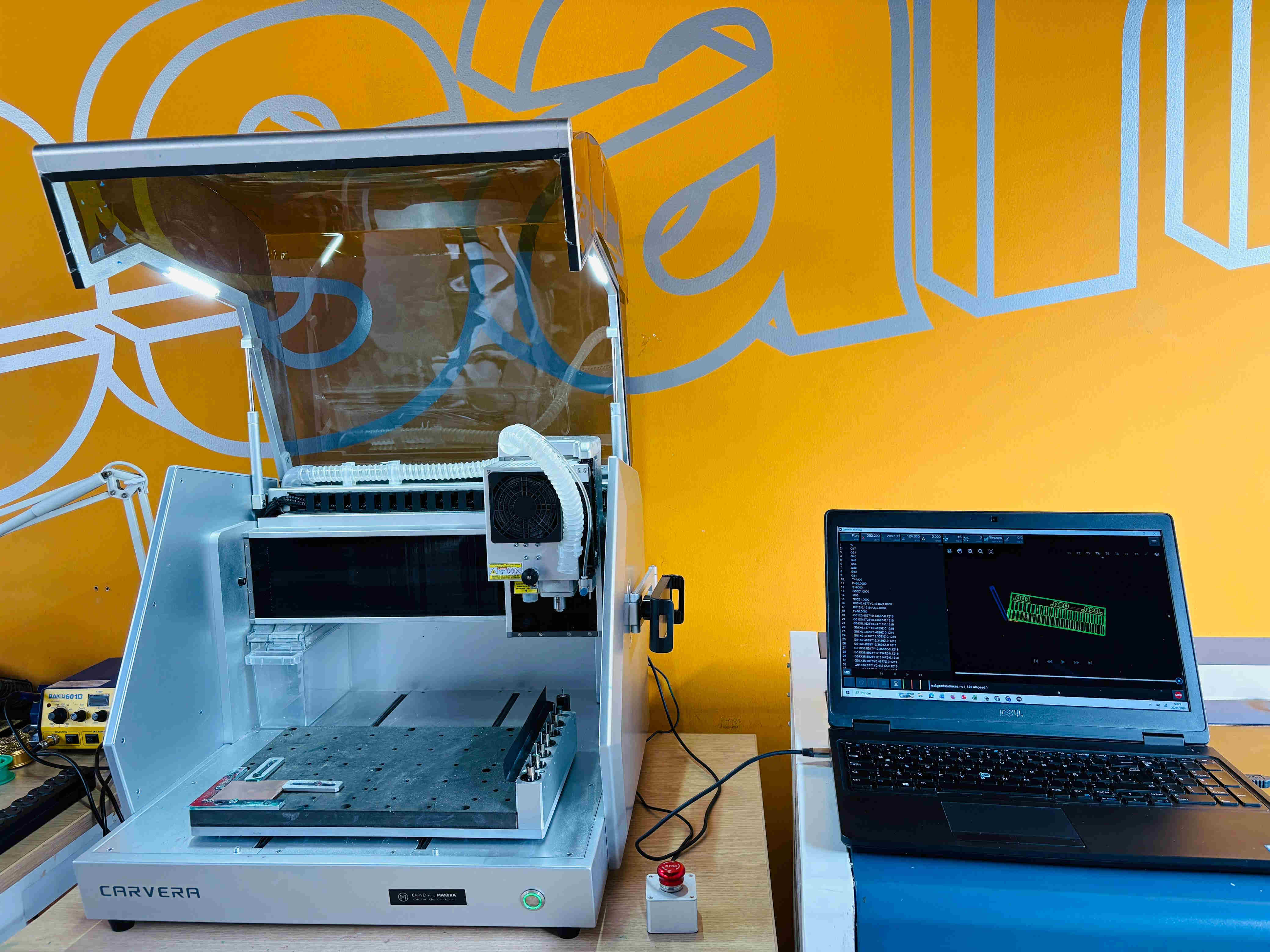
The machine we use for PCB fabrication is the Carvera by Makera— a compact, professional CNC mill designed for precision work. It connects to a laptop via USB and is controlled through the Carvera Controller software, where toolpaths are loaded and the milling process is monitored in real time.
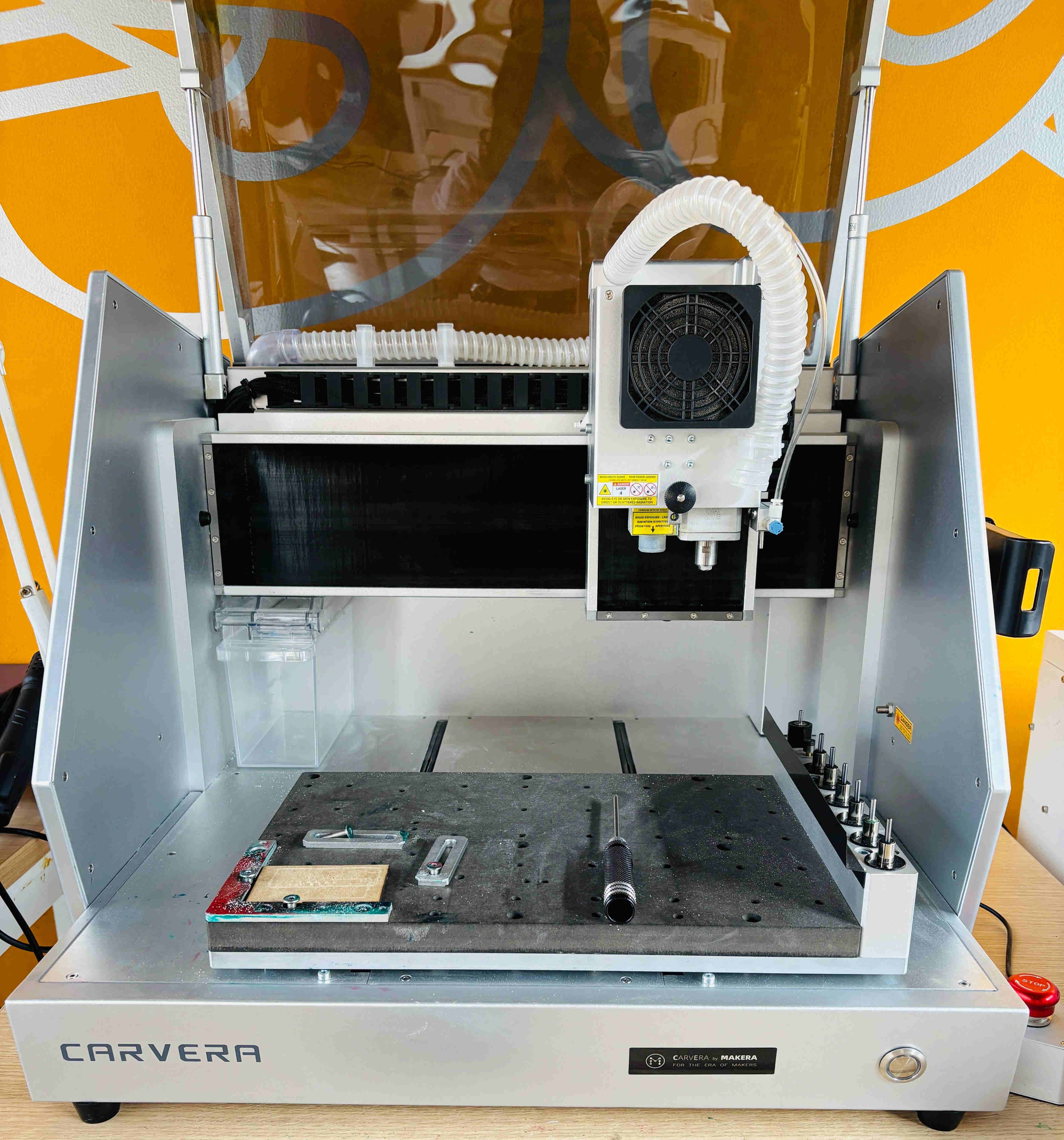
| Feature | Value | What it means |
|---|---|---|
| Work area | 360 × 240 × 140 mm | Maximum space available for milling — more than enough for PCBs |
| Resolution | 0.01mm | Minimum movement precision — essential for fine traces |
| Spindle speed | 0 – 15,000 RPM | Rotation speed of the bit — adjusts depending on material and tool |
These specifications are important for PCB production because precision is critical — even a small mistake in depth or positioning can damage traces or create short circuits. Two features of the Makera Carvera make the process much more reliable, particularly for first-time PCB fabrication:
Auto probing and leveling
Before milling, the Carvera automatically measures the board surface at multiple points and compensates for any small irregularities. This ensures the bit cuts at the same depth across the entire board, even if the surface is not perfectly flat after sanding.
Automatic Tool Changer
The Carvera switches from the trace bit to the outline bit automatically, without any manual intervention. This reduces the chance of errors when changing tools mid-process.
The Tools
Two different bits are used depending on the operation:
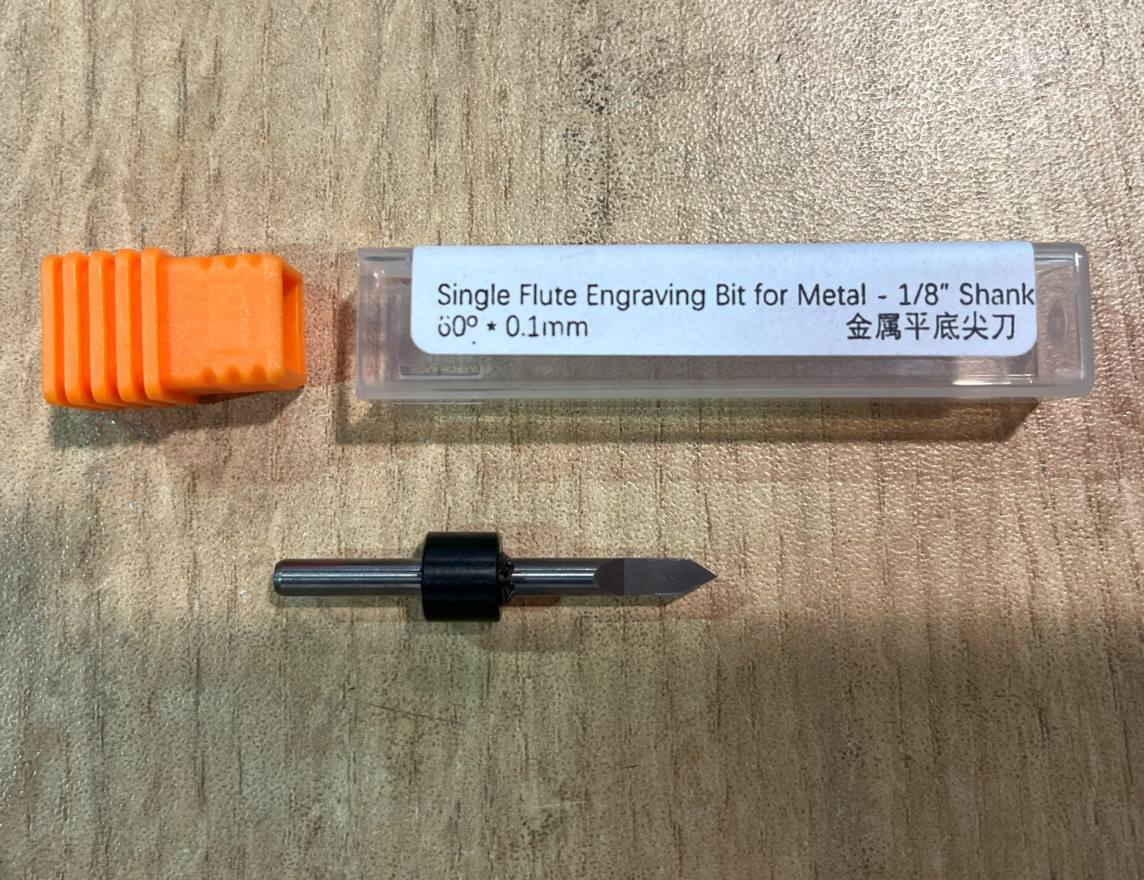
Tool 4 — For traces
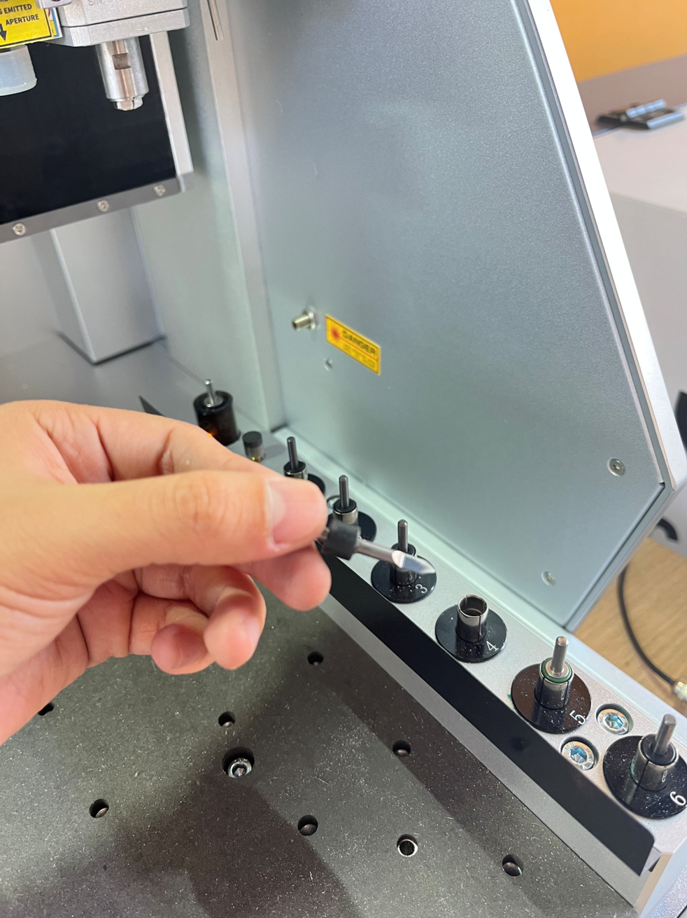
Single Flute Engraving Bit for Metal — 60° × 0.1mm tip, 1/8" shank
This V-shaped bit is used to mill the copper traces. Its very fine tip allows it to cut precise, narrow paths between traces without damaging adjacent copper.
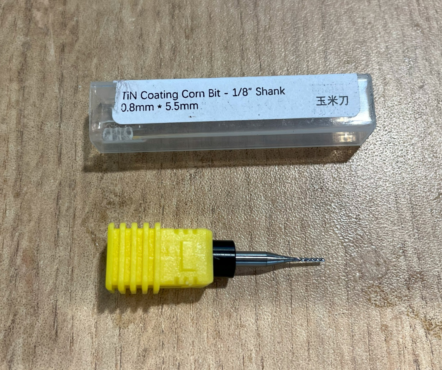
Tool 3 — For outline
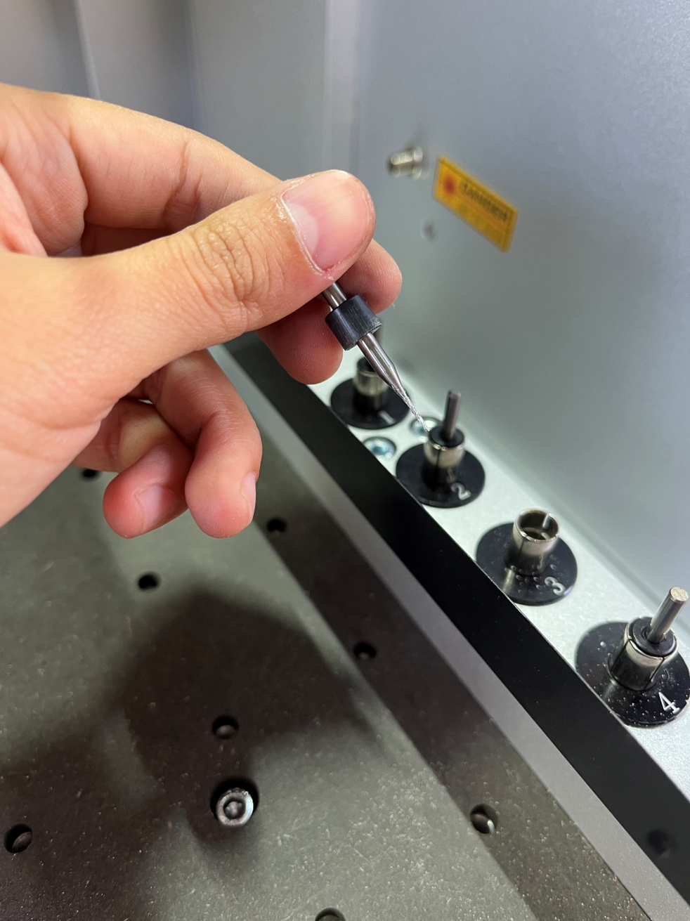
TiN Coating Corn Bit — 0.8mm × 5.5mm, 1/8" shank
This cylindrical bit is used to cut the board outline. It is more robust than the engraving bit and can cut through the full thickness of the PCB in multiple passes.
Materials Needed
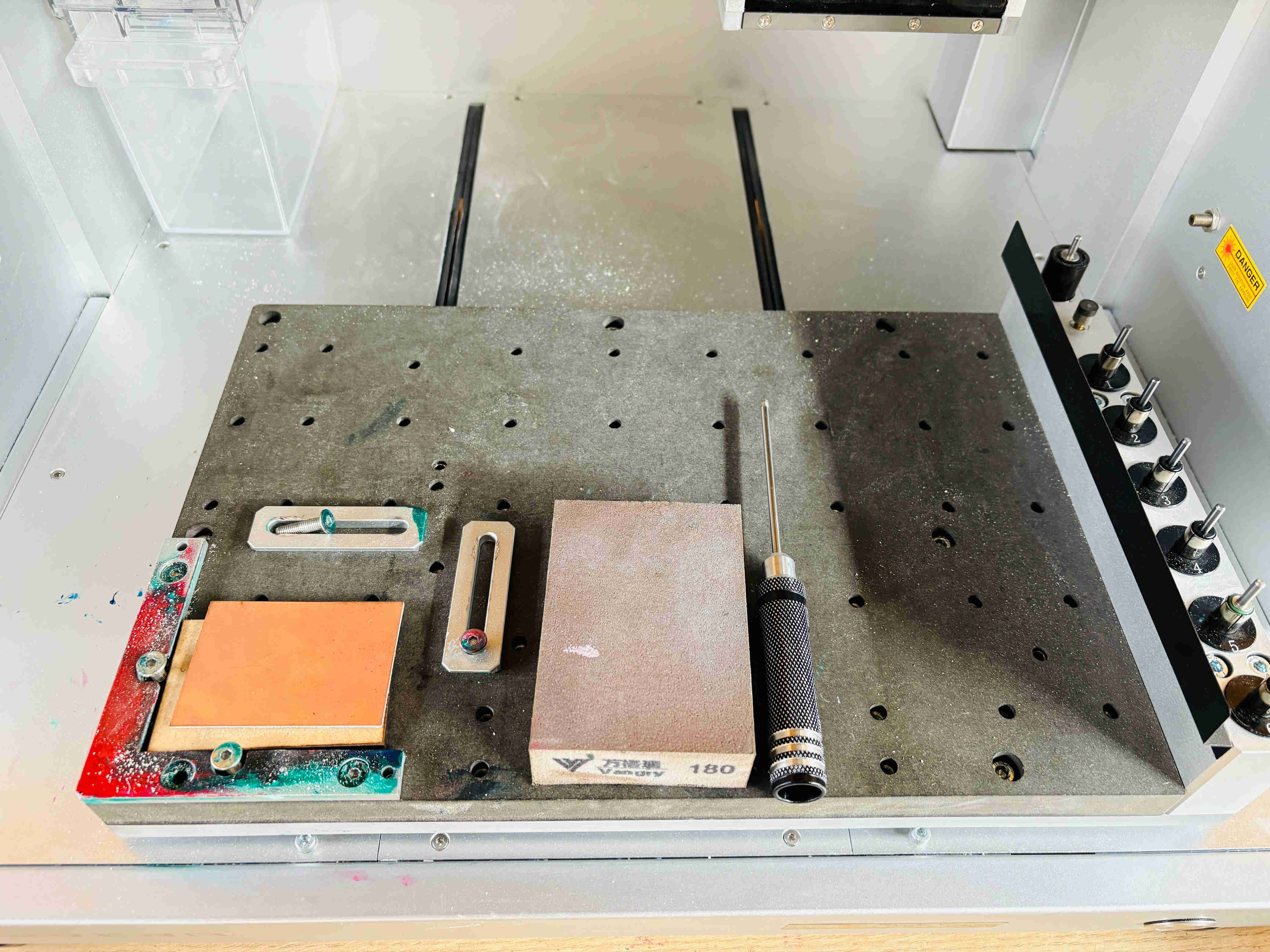
Before starting the milling process, the following materials are required:
- Copper PCB blank — the base material where the circuit will be milled
- MDF board — placed underneath to protect the machine bed and allow the outline cut to go all the way through
- Screws and metal clamps — to secure the board so it does not move during milling
- Screwdriver — to tighten the clamps
- Sandpaper 180 grit — to prepare the copper surface before milling
- Mini vacuum cleaner — to remove copper dust between operations
Preparing the Board
Before placing the board in the machine, the copper surface needs to be sanded with 180 grit sandpaper. This step is easy to overlook but very important — the copper surface is rarely perfectly flat. Even small irregularities can cause the engraving bit to cut at different depths across the board, resulting in traces that are too shallow in some areas and too deep in others. Sanding ensures a uniform surface so the bit cuts consistently.
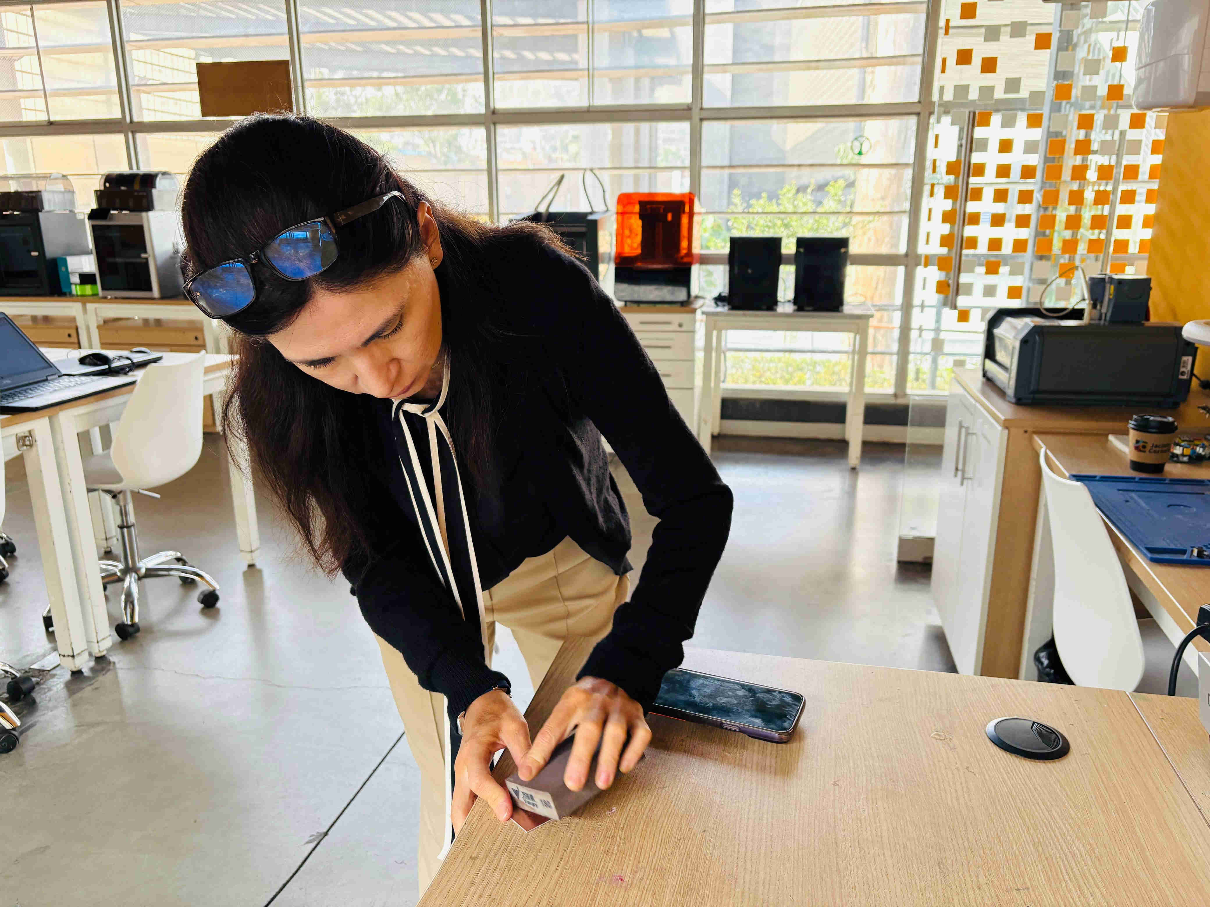
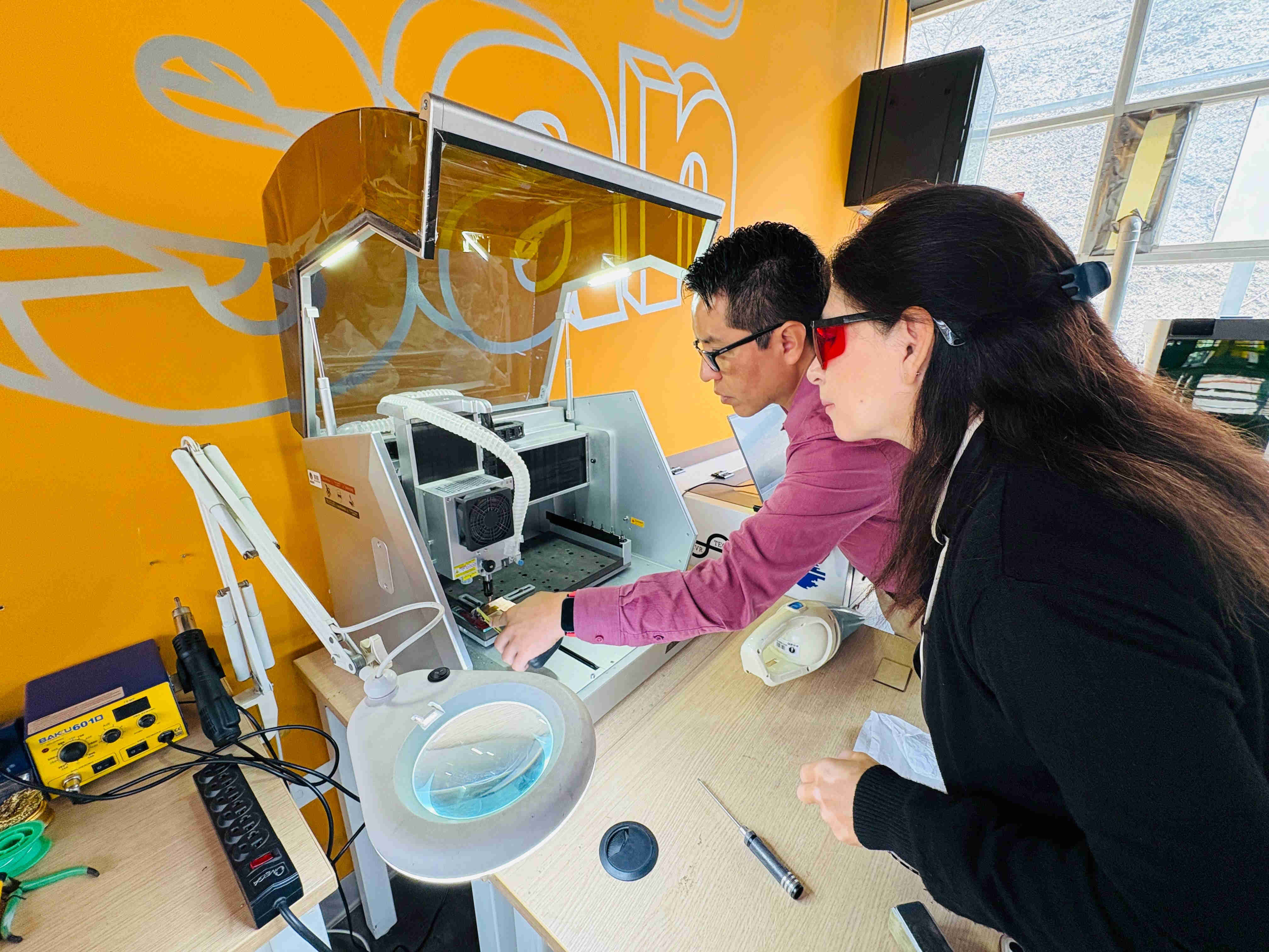
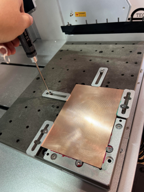
Once sanded, the board is placed on top of the MDF and secured to the machine bed using the metal clamps and screws. It is important to tighten them firmly — any movement during milling will ruin the traces.
Configuring the Toolpaths in ModsProject
With the board ready, the next step is generating the toolpaths using ModsProject — a browser-based CAM tool. It takes PNG images of the PCB design and converts them into 📁 .nc files (G-code) that the Carvera Controller can read.
If you only have Gerber files from KiCad, you can convert them to PNG first using Gerber2PNG — a free online tool that generates the images needed for ModsProject.
This process is done twice — once for the traces and once for the outline cut.
1. Select the machine
When opening ModsProject, the first step is selecting the correct machine. In our case we selected Carvera Controller from the machine list. This loads the correct workflow and settings for our machine.
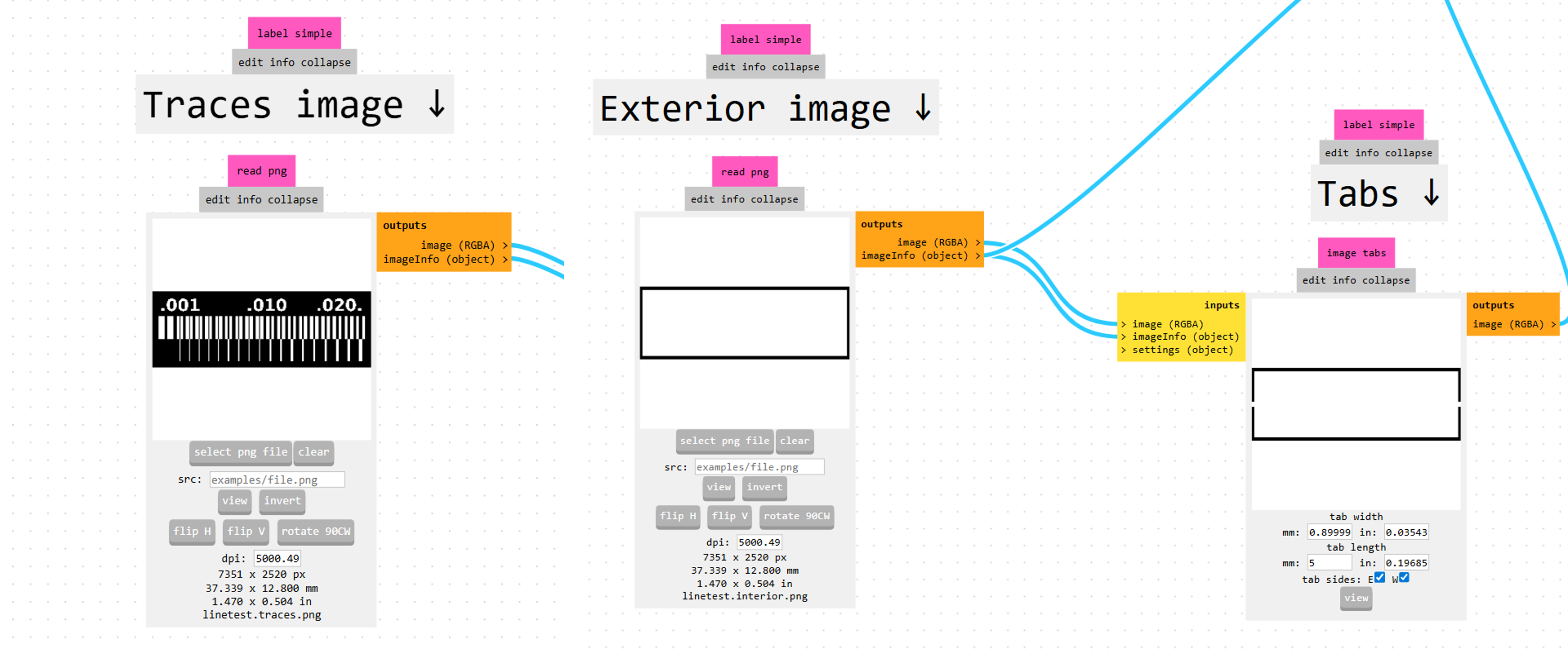
2. Load the Traces image
The traces PNG is loaded into the Traces image section. This image tells the machine exactly where to mill the copper to create the circuit traces — ModsProject reads it and translates it into movements the Carvera can execute.
3. Load the Exterior image and configure Tabs
The outline PNG is loaded into the Exterior image section. This is also where the Tabs are configured — small bridges of material that keep the board attached to the copper sheet during the outline cut. Without tabs, the board could shift or fly off the moment it is fully cut through, ruining the result.
4. Configure the tool parameters
Once both images are loaded, the tool parameters are configured in the mill dual-tool 2D section. These settings tell the machine exactly how deep to cut and how wide each pass should be:
| Tool 4 — Traces | ||
|---|---|---|
| Parameter | Value | What it means |
| Tool diameter | 0.4mm | Effective cut width with the 60° V-bit at this depth |
| Cut depth | 0.12mm | How deep the bit goes — enough to cut through the copper layer |
| Max depth | 0.12mm | Total depth — single pass is enough for traces |
| Offset number | 2 | Two passes around each trace for cleaner, more defined edges |
| Offset stepover | 0.5 | 50% overlap between passes — no gaps left uncut |
| Tool 3 — Outline | ||
|---|---|---|
| Parameter | Value | What it means |
| Tool diameter | 0.8mm | Actual diameter of the cylindrical corn bit |
| Cut depth | 0.6mm | Depth per pass — multiple passes needed to cut the full board |
| Max depth | 1.75mm | Total depth — cuts through the full PCB thickness plus a margin |
| Offset number | 1 | Single pass around the outline is enough |
| Offset stepover | 0.5 | 50% overlap between passes |
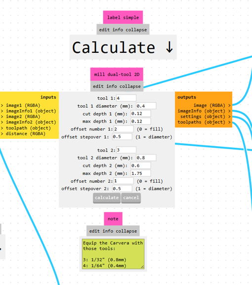
📝 The note in ModsProject also reminds which physical tools to load in the Carvera:
🖰 Tool 3→ 1/32" (0.8mm) corn bit → outline🖰 Tool 4→ 1/64" (0.4mm) engraving bit → traces
5. Calculate and export
After clicking 🖰 Calculate , ModsProject generates the toolpaths and exports two separate 📁 .nc files — one for the traces and one for the outline. Each file is loaded into the Carvera Controller separately and run in order: traces first, then outline.
The Milling Process
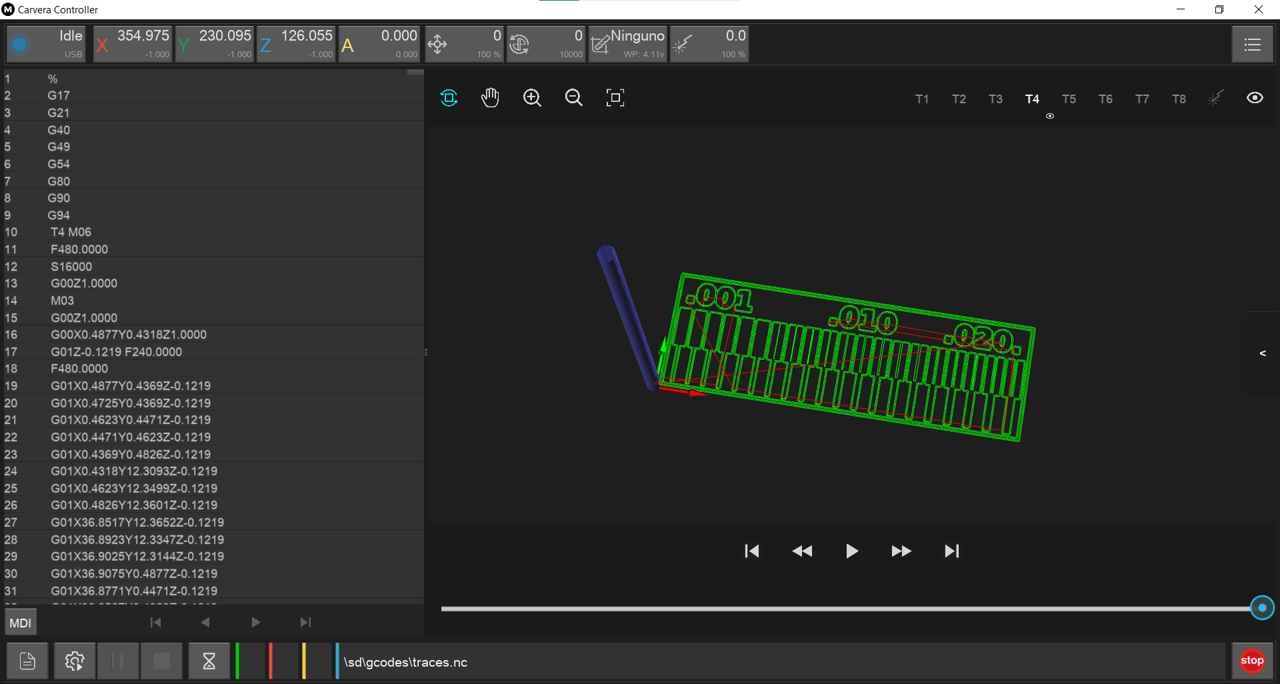
The milling process follows a specific order that is important to respect. The first step is connecting the laptop to the Carvera via USB and opening the Carvera Controller software. Once connected, the 📁 .nc file for the traces is loaded into the software.
1. Calibrate the machine
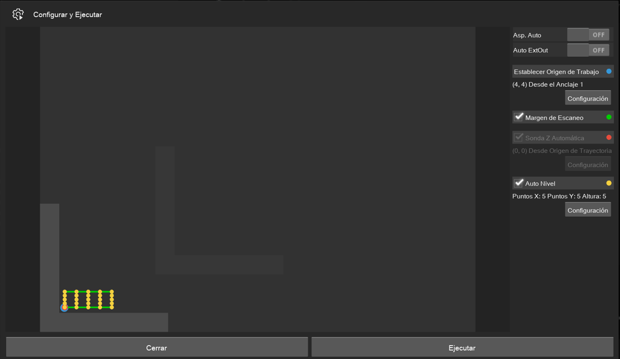
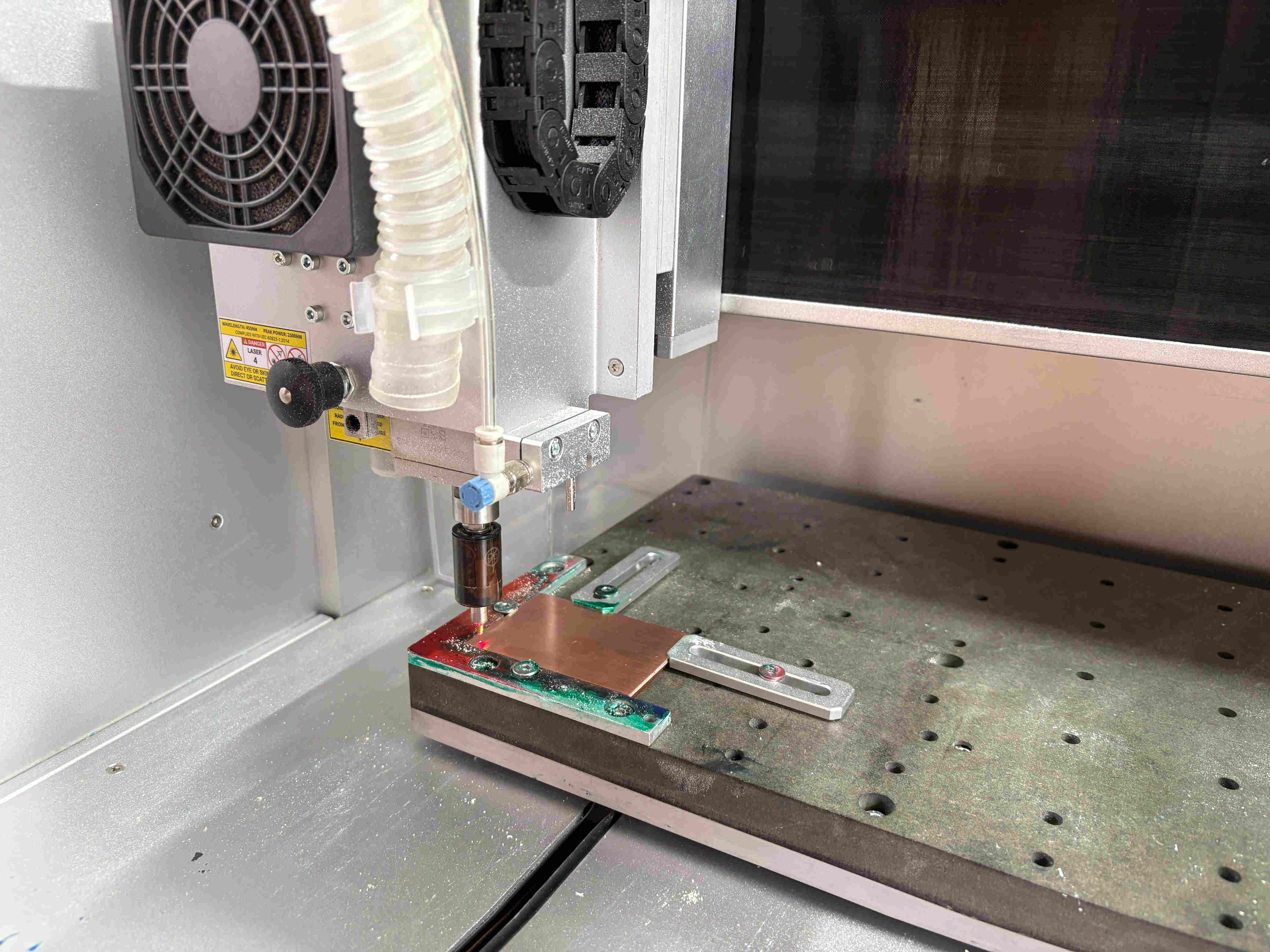
Before running any file, the Carvera needs to be calibrated. This is done automatically by the machine — it probes the surface of the copper board at multiple points to map any small height variations and compensate for them. This step is configured in the software before clicking run, and it ensures the bit cuts at the correct depth across the entire board.
2. Mill the traces
Once calibration is complete, click 🖰 Run and the Carvera starts milling the traces with Tool 4. The machine works through the entire toolpath automatically — no manual intervention is needed while it runs.
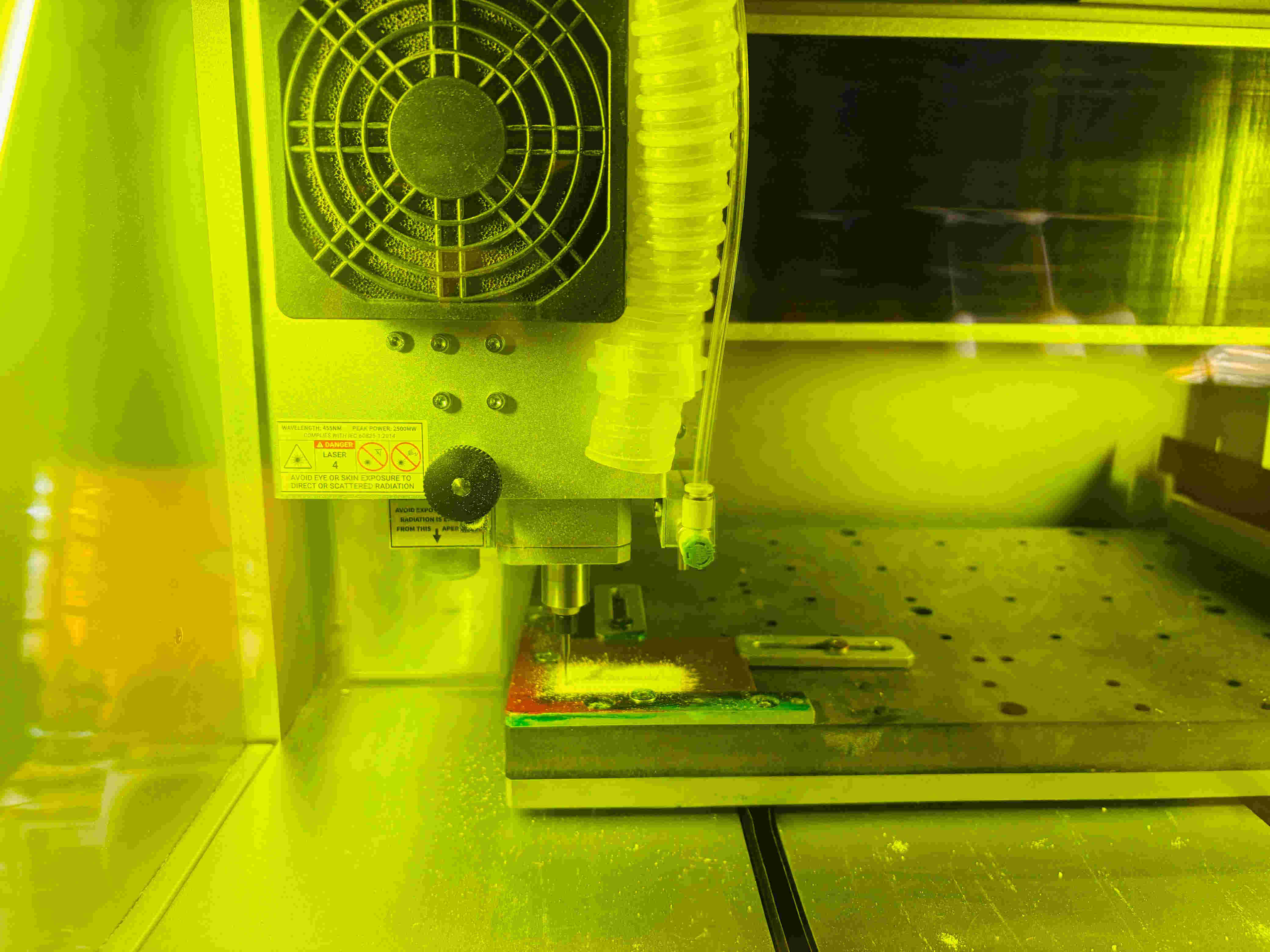
3. Vacuum the copper dust
After the traces are milled, copper dust is left on the surface of the board. This must be vacuumed before continuing — copper dust can interfere with the outline cut and is also harmful to inhale.
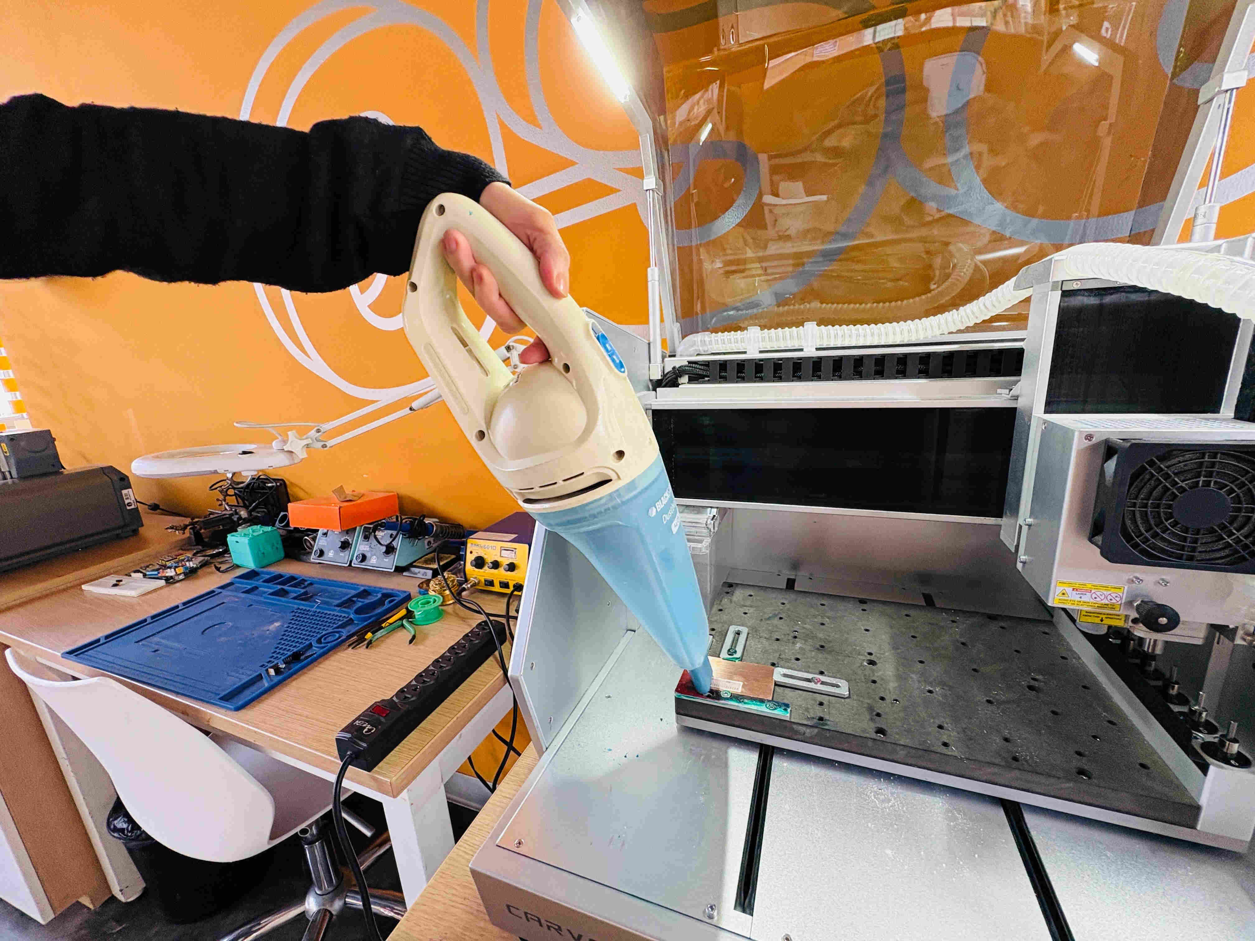
4. Mill the outline
The outline 📁 .nc file is now loaded into the Carvera Controller. The same calibration process runs automatically before cutting begins. Once ready, click 🖰 Run and the Carvera cuts the board outline with Tool 3 in multiple passes until it goes all the way through.
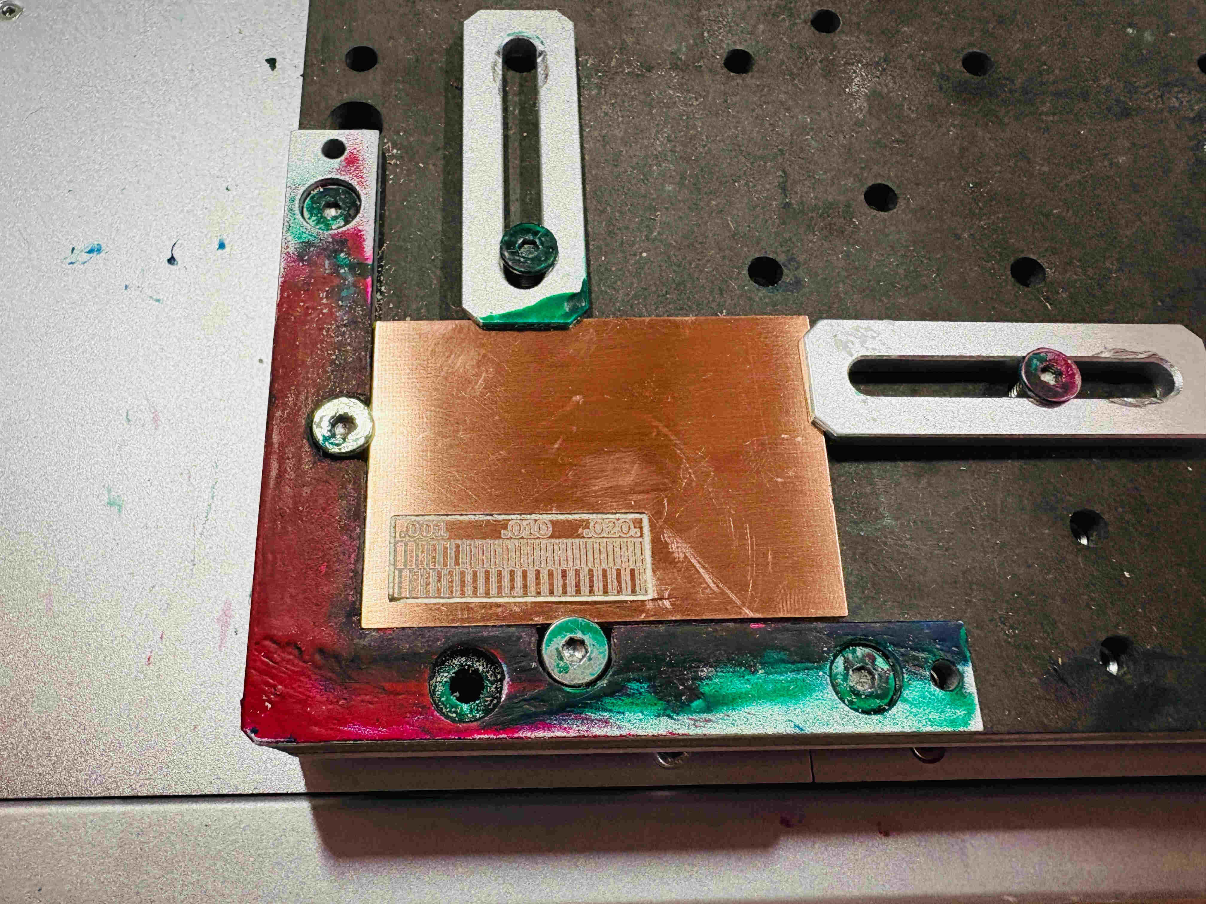
5. Vacuum and remove the board
Once the outline cut is complete, vacuum the remaining dust and carefully remove the board from the machine. The tabs that were configured in ModsProject will still be holding the board in place — these need to be carefully cut or broken to release the piece.
6. Final sanding
After removing the board, a light sanding is done to clean up any rough edges left by the tabs and to remove any remaining copper debris from the surface. This leaves the board clean and ready for inspection and soldering.
⚠️ IMPORTANT: The order matters — traces always go first. If the outline is cut first, the board can shift and the traces will be completely misaligned.
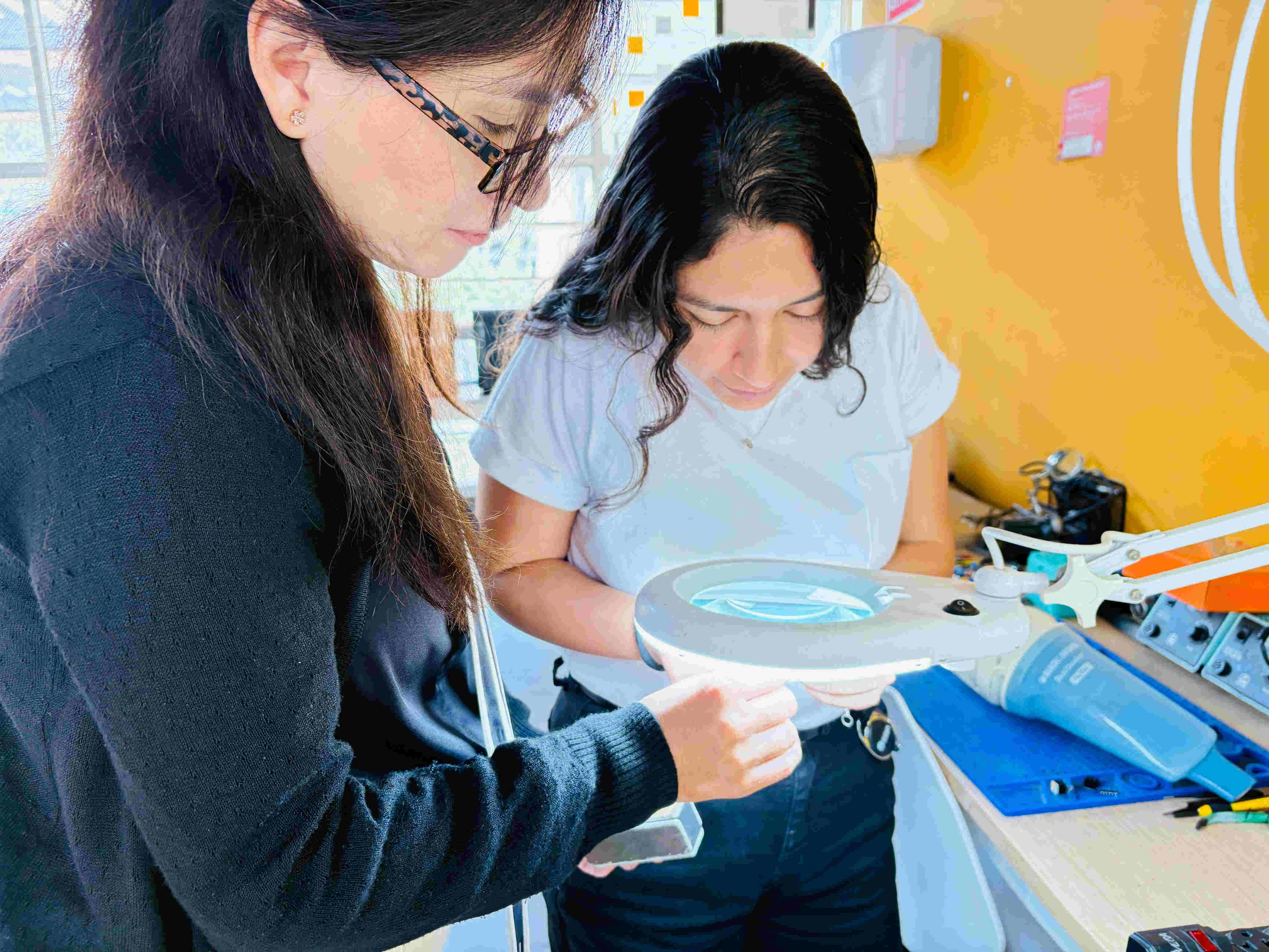
Characterization — The Line Test
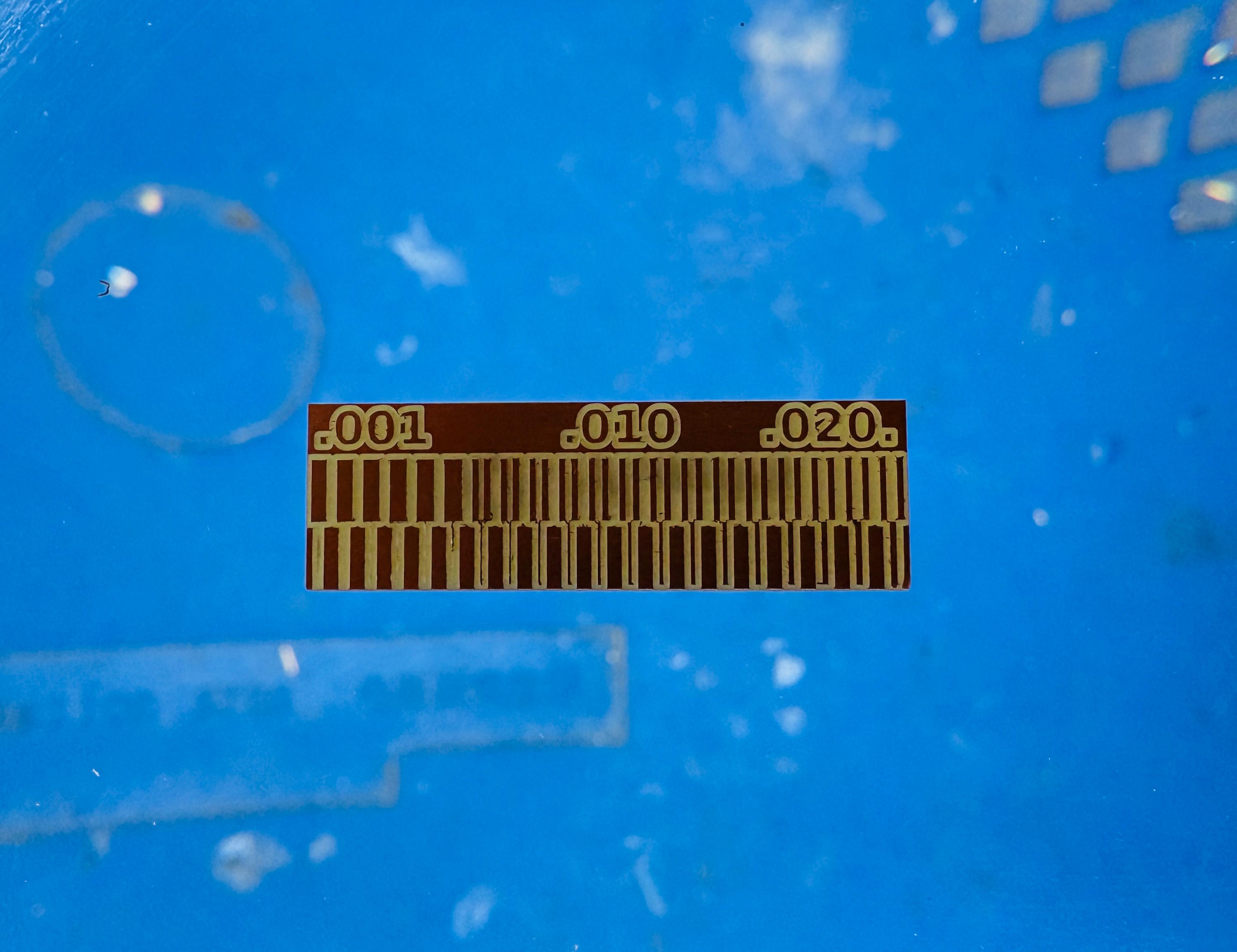
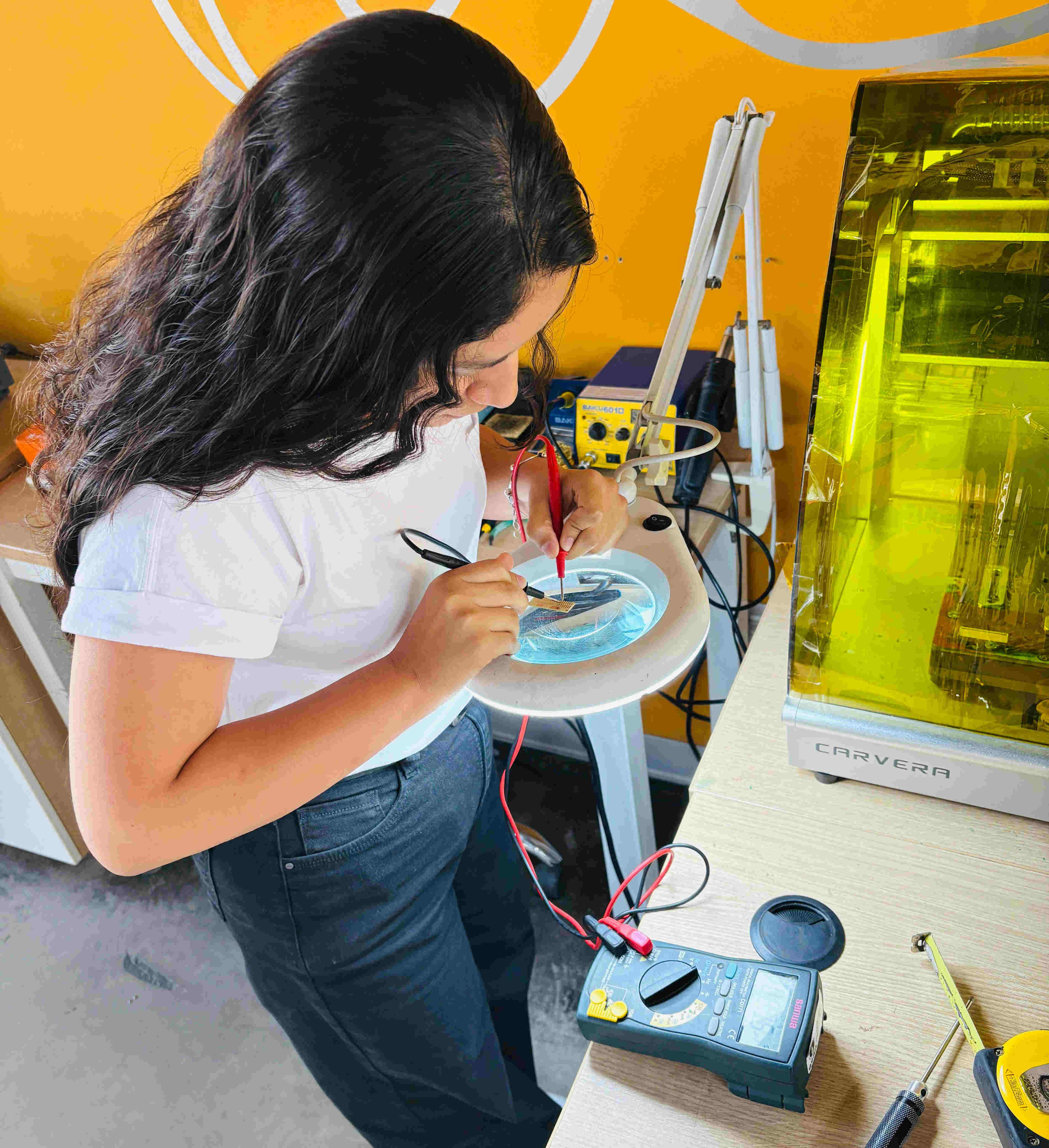
Before milling any real PCB, we ran a line test — a standard procedure to determine the minimum trace width the machine can produce reliably with these settings and tools. The line test is a pattern of copper traces with increasing widths, ranging from .001" (0.025mm) to .020" (0.508mm). After milling, the result is inspected visually and with a multimeter to find where traces are clearly separated and electrically isolated.
| Trace width | Result |
|---|---|
| .001" — .006" (0.025–0.15mm) | ❌ Traces merged — not reliable |
| .007" (0.178mm) | ⚠️ Borderline — barely visible separation |
| .008" — .010" (0.2–0.254mm) | ✅ Acceptable |
| .010" — .020" (0.254–0.508mm) | ✅ Excellent — well defined |
Results
The table shows which trace widths the machine can produce reliably and which ones are too fine. Traces below .007" were not well separated, meaning they could potentially create short circuits on a real PCB. From .008" upward, the separation was clear and consistent.
Minimum recommended trace width: 0.2mm (.008") using the Single Flute Engraving Bit 60° × 0.1mm on the Makera Carvera.
This test helped verify that our PCB designs were within a safe manufacturing range. The signal traces were already designed at 0.4mm and the power traces at 0.8mm, both comfortably above the reliable limit confirmed by the line test.
Sending a PCB to a Boardhouse — JLCPCB 🏠
For this assignment we documented the workflow using JLCPCB, one of the most popular and affordable PCB manufacturing services used by Fab Academy students worldwide.
What is JLCPCB?
JLCPCB is an online PCB manufacturing service that allows you to upload your design files and receive professionally fabricated boards delivered to your door. It supports a wide range of specifications, quantities, and finishes.
The Workflow
1. Create an account
The first step is creating an account on the JLCPCB website. You can sign up using your email address. After logging in, you may be asked to complete some basic profile information before placing an order.
2. Start a new order and upload the Gerber files
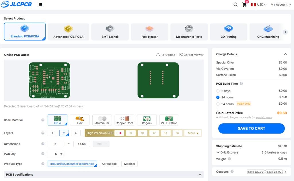
To start a new order, click 🖰 Add Gerber File. JLCPCB accepts Gerber files compressed in a 📁 .zip folder — this is the standard export format from KiCad. Once uploaded, the platform automatically reads the files and generates a preview of your board.
3. Review the board preview and DFM Check
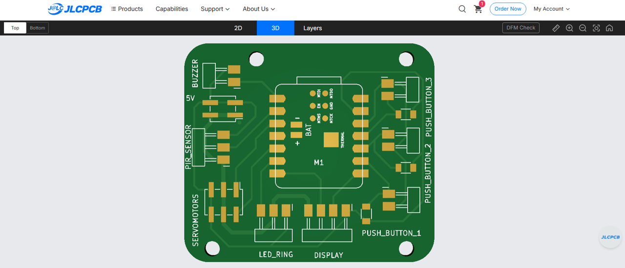
After uploading, JLCPCB shows a preview of your board including a 2D view, 3D view, and individual layer views. It also runs a DFM Check (Design for Manufacturability) — similar to the DRC in KiCad — which verifies that your design meets the minimum manufacturing requirements. This is a useful check before placing the order. In our case the board was detected as a 2-layer board of 44.54 × 51mm.
4. Configure the order
JLCPCB offers a wide range of options to customize the order. Here is an overview of the most relevant ones:
| Option | What it means |
|---|---|
| Base Material | The type of PCB substrate — FR-4 is the standard option for most projects |
| Layers | Number of copper layers — 2 is standard for most designs |
| Dimensions | Automatically detected from the Gerber files |
| PCB Qty | Minimum order is 5 units |
| Product Type | Category of the board — Industrial/Consumer electronics for most cases |
| PCB Thickness | Standard is 1.6mm |
| PCB Color | The solder mask color — green is default, other colors available |
| Silkscreen | The color of the text and labels printed on the board |
| Surface Finish | How the exposed copper pads are treated — HASL is the standard option |
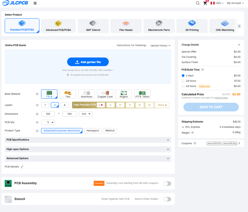
Beyond these basic options, JLCPCB also offers:
- PCB Assembly — they can source and solder the components onto your board for an additional cost
- Stencil — a metal stencil for applying solder paste if you want to do your own assembly
5. Review the price and save to cart
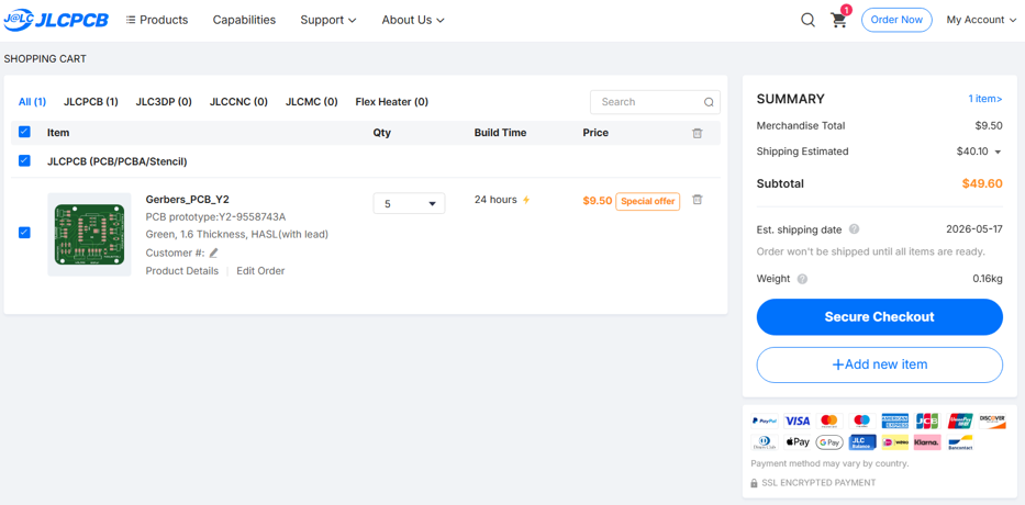
For this exercise we kept the default settings and selected 24-hour build time for faster fabrication. Adding the boards to the cart shows the full order summary — board specs confirmed as Green, 1.6mm thickness, HASL finish, 5 units.
Testing the fastest available shipping option to Peru via DHL Express, the estimated delivery time is 3 to 6 business days. The order is ready to be placed.
| Item | Cost |
|---|---|
| PCB fabrication (5 units) | $9.50 |
| Shipping (DHL Express, 3-6 days) | $40.10 |
| Subtotal | $49.60 |
What I Learned
This week I learned that the PCB milling workflow depends a lot on correct preparation before the machine even starts cutting. Going from Gerber files to PNG images, configuring the tools in ModsProject, and generating the G-code made the whole process feel much more practical and connected.
The line test was especially useful because it helped us understand the real limits of the machine and tools before milling the final board. It also confirmed that our design was within a safe manufacturing range.
I also learned that each tool requires different configurations, and using incorrect parameters can affect the milling result or even damage the bit. Another important step was verifying the traces with a multimeter to check continuity and confirm that there were no unwanted connections between traces.
For the boardhouse workflow, using JLCPCB was straightforward once the Gerber files were ready. One thing I noticed was that the minimum order is 5 boards, and the shipping cost to Peru was much higher than the fabrication cost itself. Because of that, using a boardhouse becomes more practical when you need boards in larger quantities.
📝 Individual Assignment:
- Make and test a microcontroller development board that you designed.
Making My Microcontroller Development Board
This week I fabricated the two boards designed during Week 6. The first board — the Brain Board — helped me understand the complete milling workflow and become familiar with each step of the process. With that experience, I then fabricated the second board — the final project board — to test and validate the updated design.
BRAIN BOARD 🧠
📄 KiCad — Gerber2PNG
To use the Carvera, we need to convert the Gerber files from the board design into PNG format. For this, I used Gerber2PNG. There, I followed these steps:
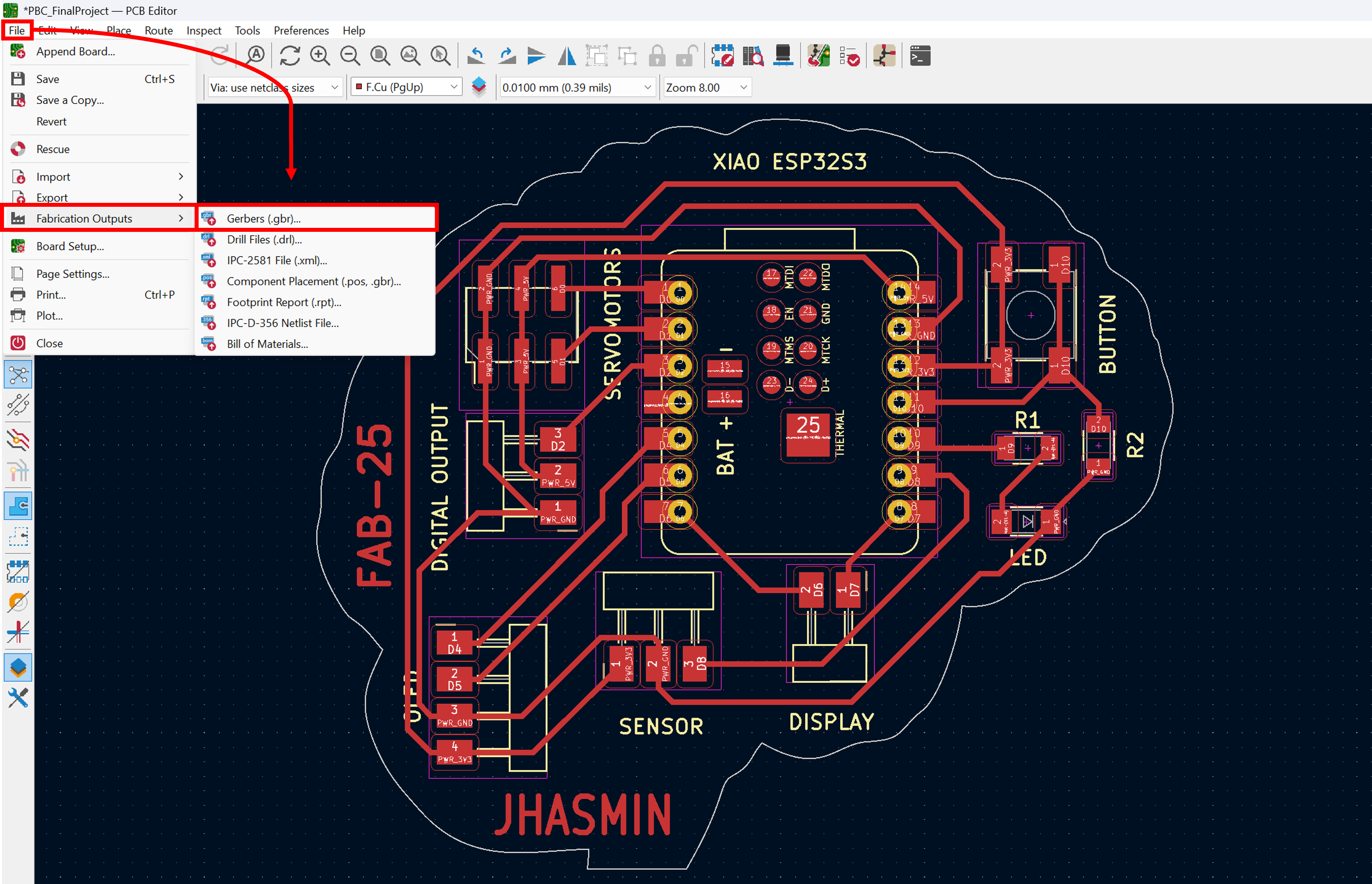
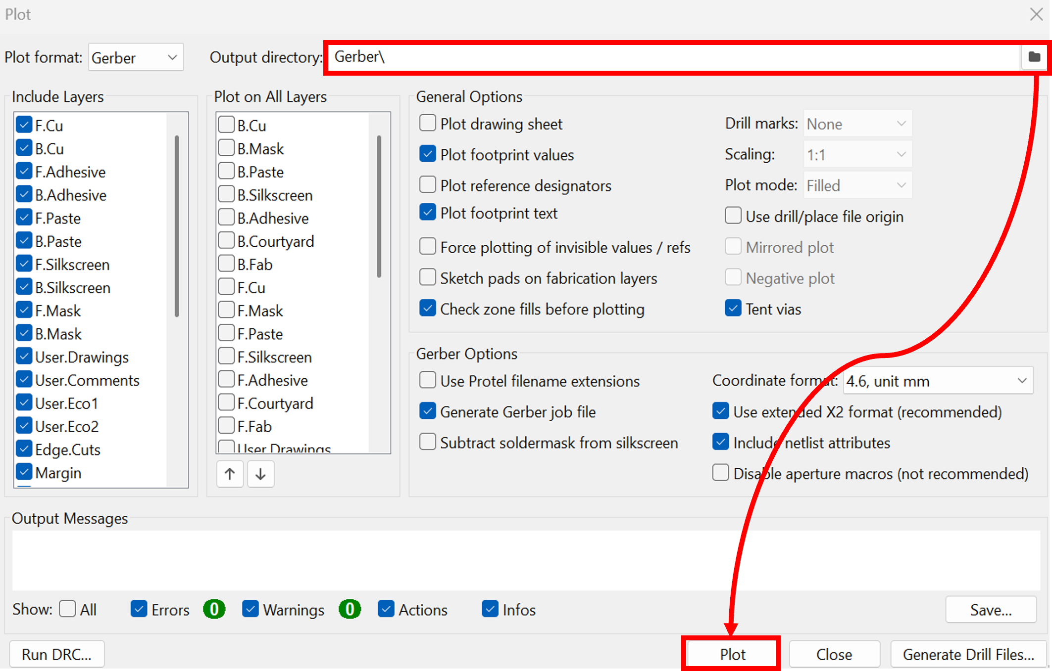
1. Export Gerber files from KiCad
I exported all Gerber files from KiCad.
2. Upload to Gerber2PNG
I dropped all the Gerber files at once into Gerber2PNG.
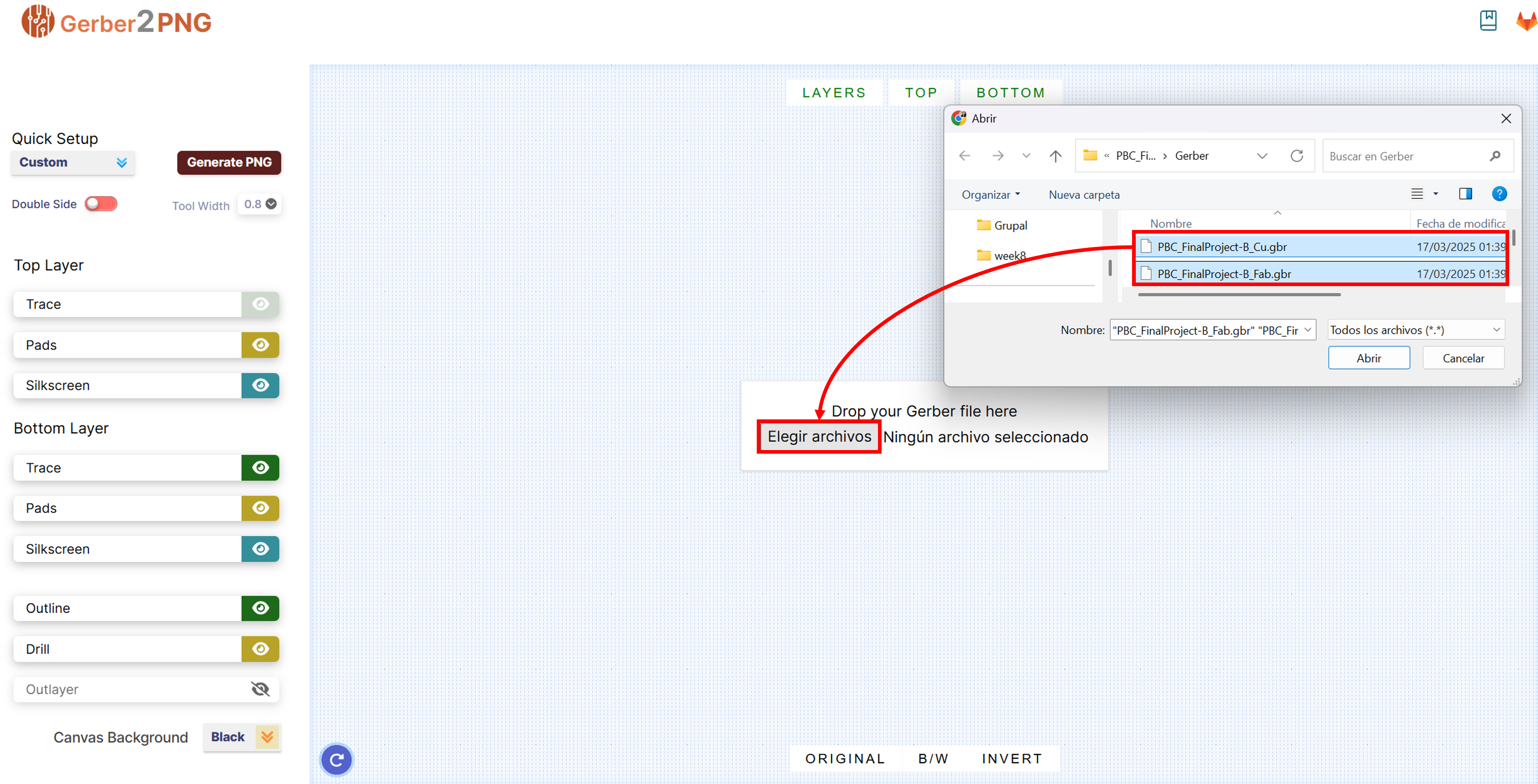
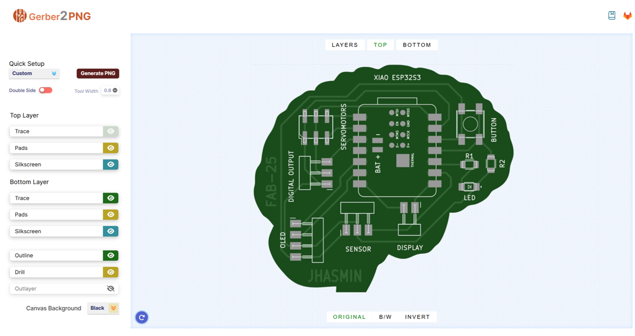
3. Select the necessary views
I selected the necessary views for board fabrication.
4. Convert to PNG format
I converted the required layers to PNG format, as Carvera requires this format in ModsProject.
5. Generate the PNG images
Then, I generated two images in Gerber2PNG: one for the traces and another for the outline cut of the shape.
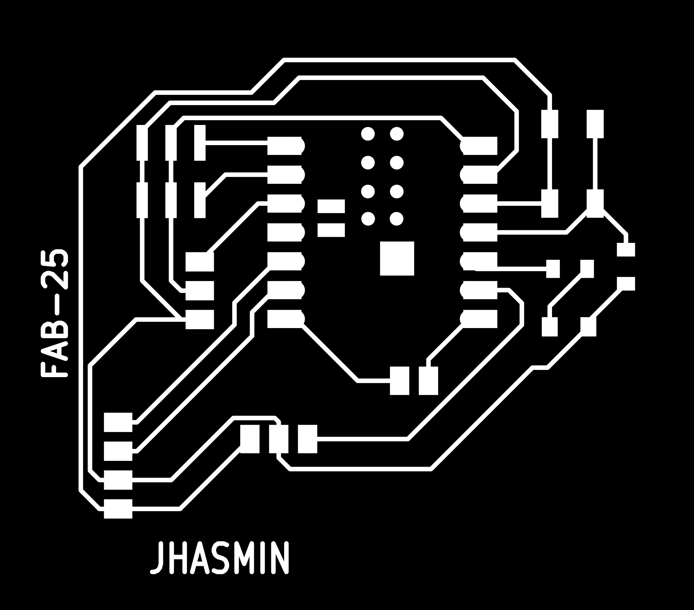
Traces

External Cut
Gerber2PNG — Mods Project
Once the Gerber files were converted to PNG, the next step was generating the files needed for the Makera Carvera. Before loading anything into the Carvera Controller, I first had to generate the G-code using Mods Project. Mods Project converts the PNG files into precise toolpaths that the machine can follow during the milling process. Before starting, I selected the correct machine configuration in Mods Project — in this case, Carvera Mill 2D PCB.
Steps to Prepare the Files for Carvera Controller:
1. Opening Mods Project and Selecting the Machine
I opened Mods Project in my browser and selected Carvera Mill 2D PCB as my machine.
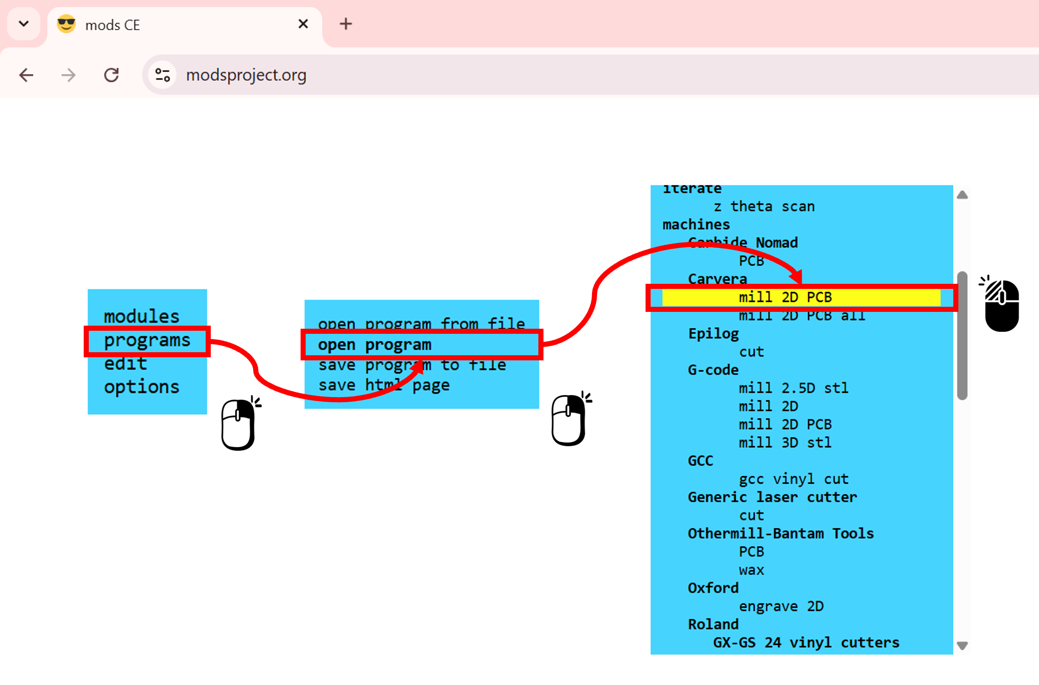
Select the machine
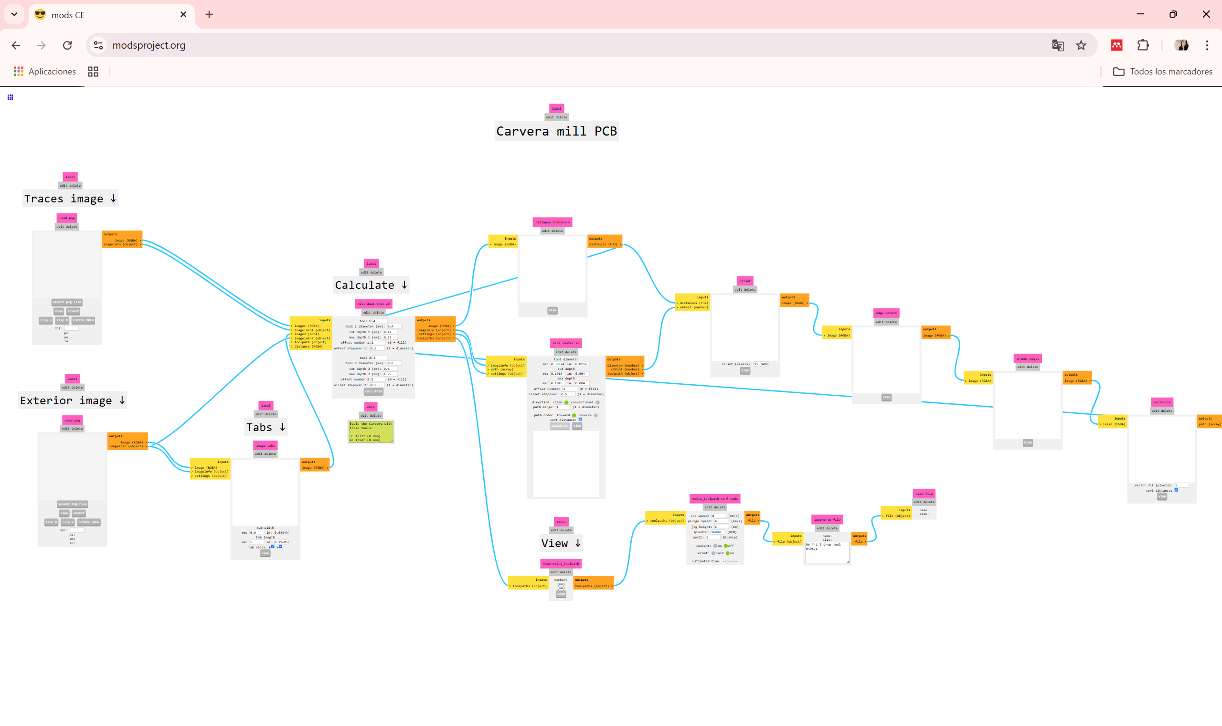
Carvera Mill PCB
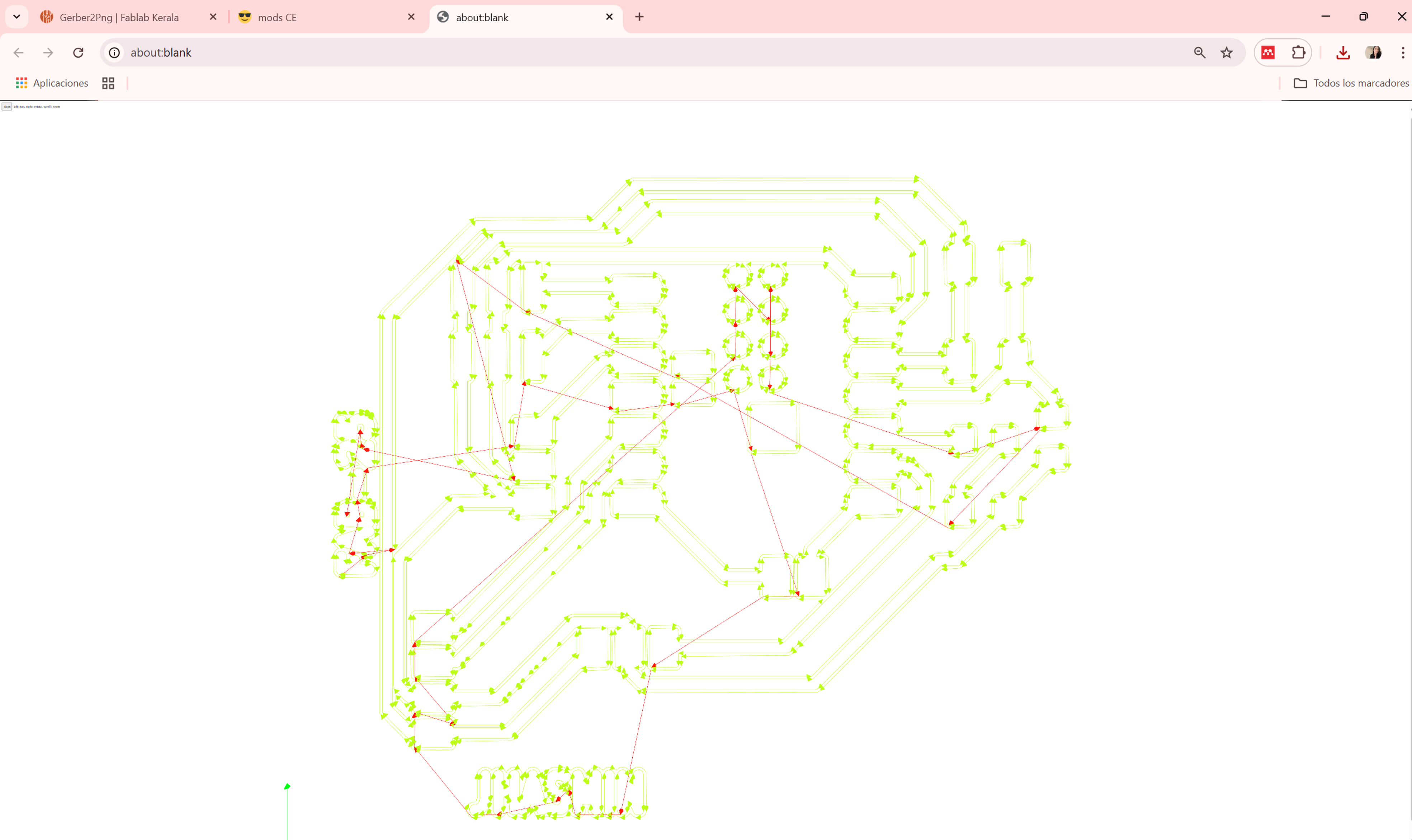
2. Generating the G-code for the Traces
I uploaded the PNG file of the traces.
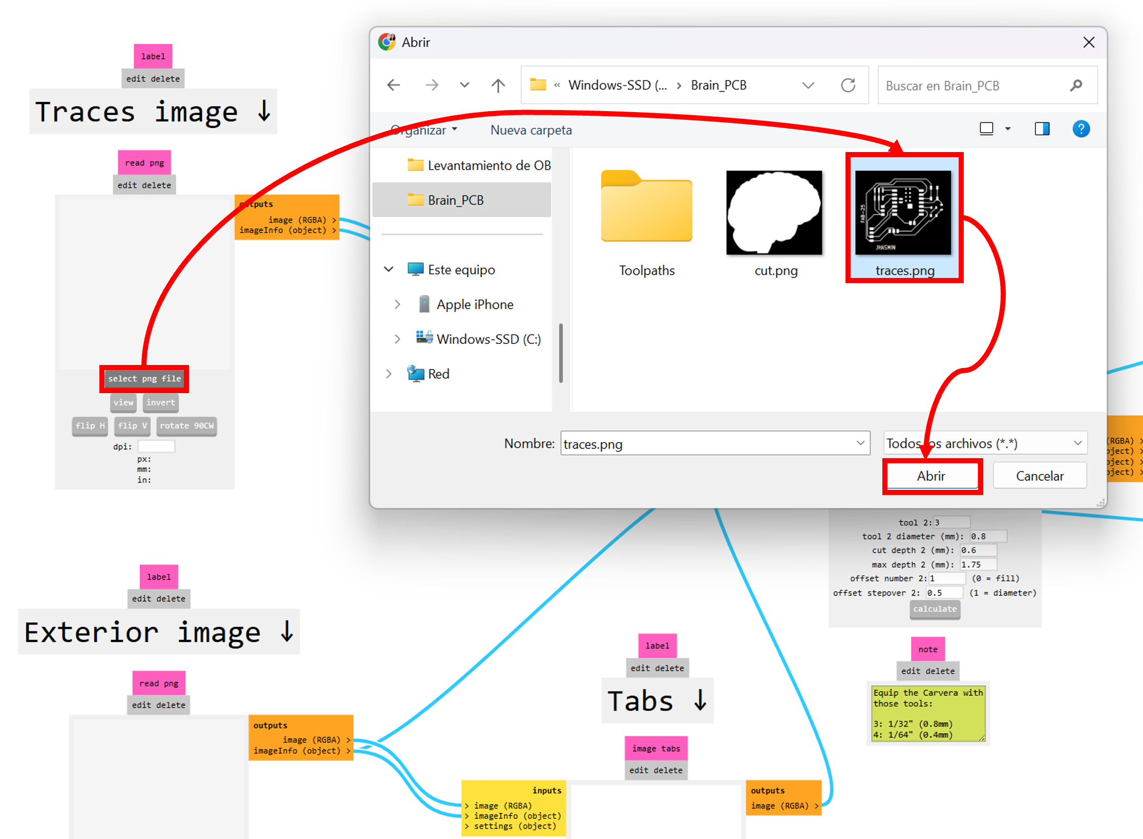
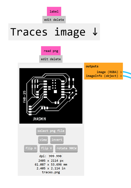
Then, I configured the parameters for the Single Flute Engraving Bit - 1/8" 60° × 0.1 mm, located in position 4 of the machine.
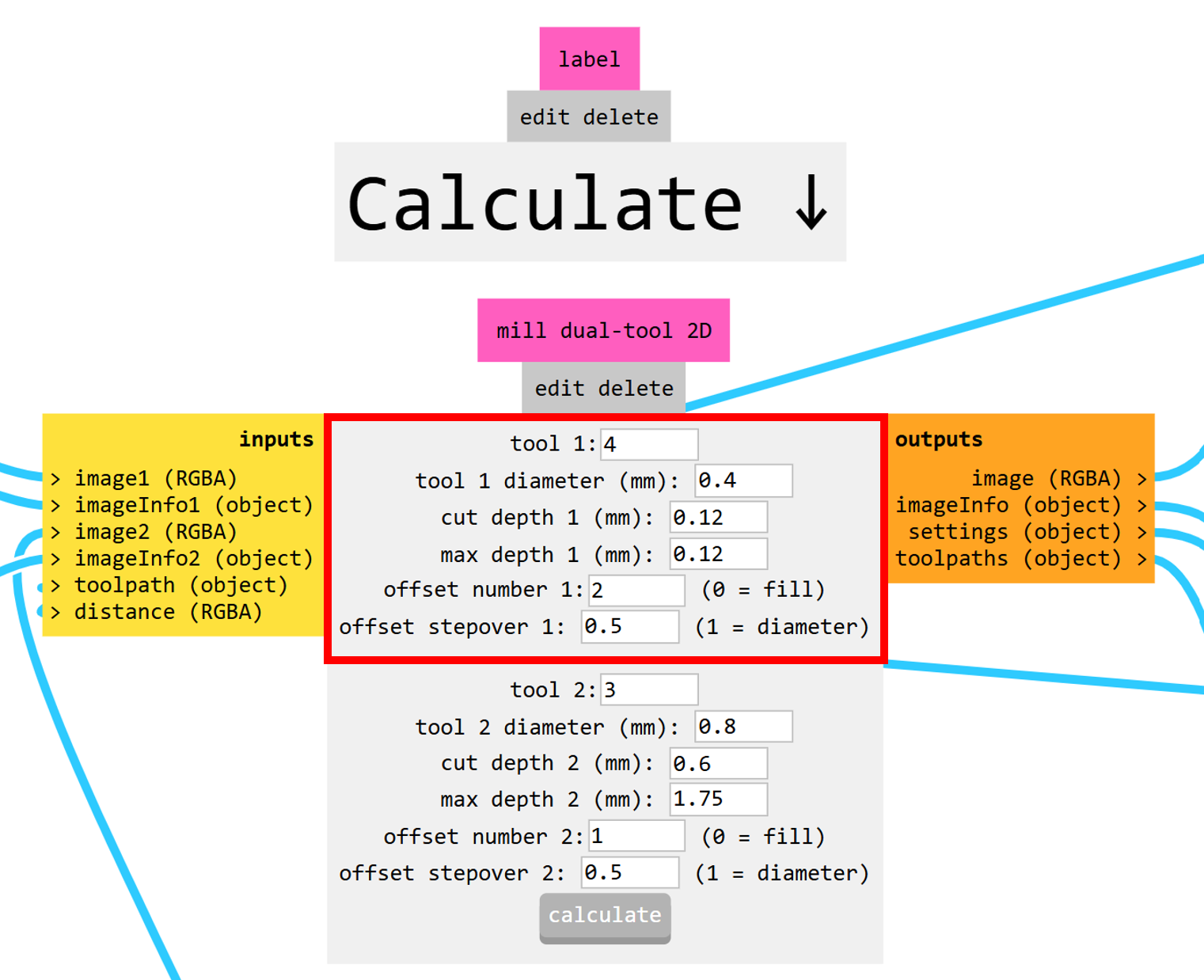
After adjusting the settings, I generated the G-code for the traces and saved it in a folder.
3. Generating the G-code for the Outline Cut
I uploaded the PNG file of the board outline.
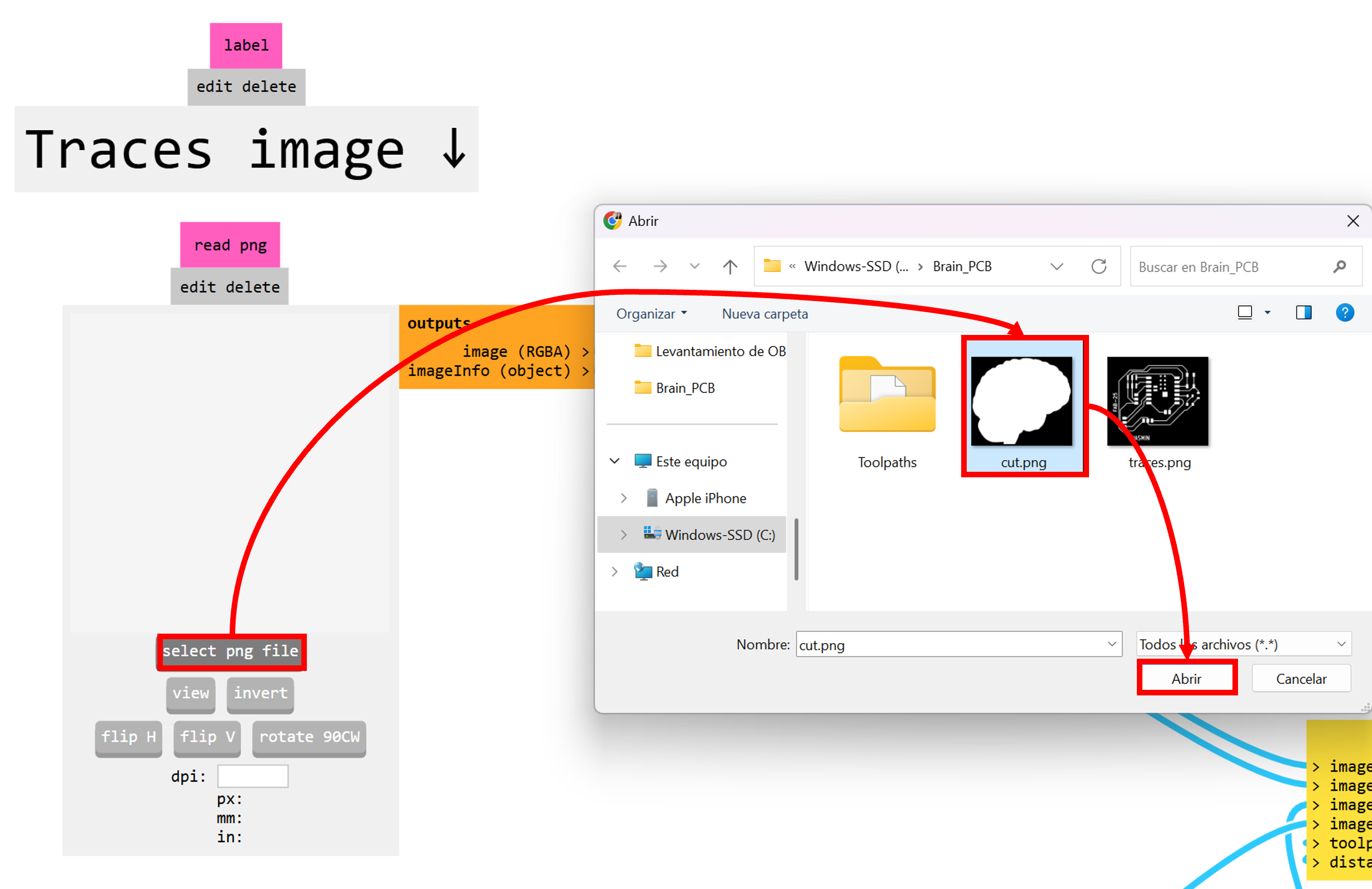
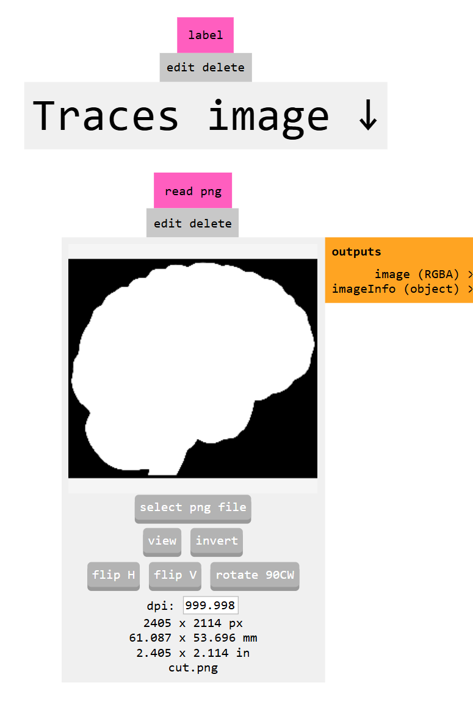
I configured the parameters for the Coating Corn Bit - 1/8" 0.8 mm × 5.5 mm, in position 3 of the machine.
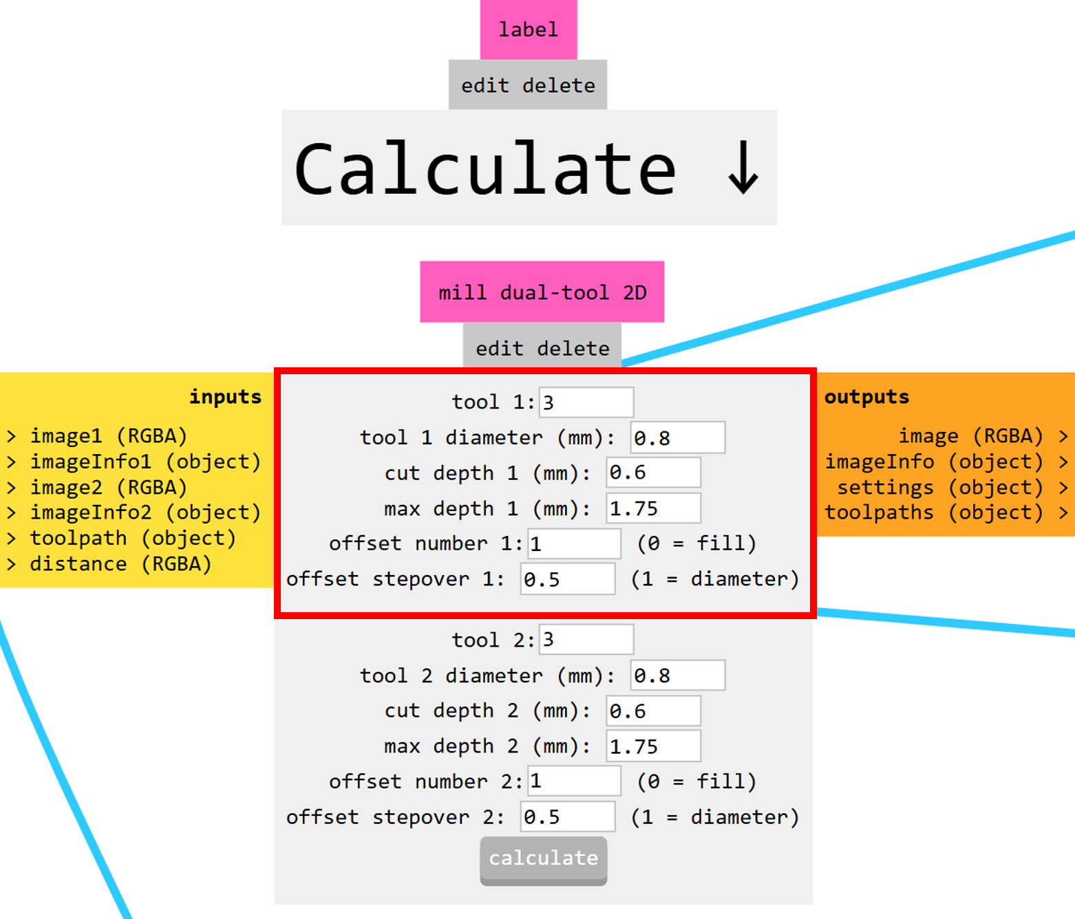
Once everything was set, I generated the G-code for the outline cut and saved it in a folder. With both G-code files ready, it was all set to load them into Carvera Controller and start the milling process!
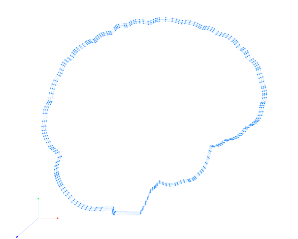
Mods Project — Carvera Controller
Steps to Prepare the Files for the Milling Process:
Traces
1. Opening Carvera Controller
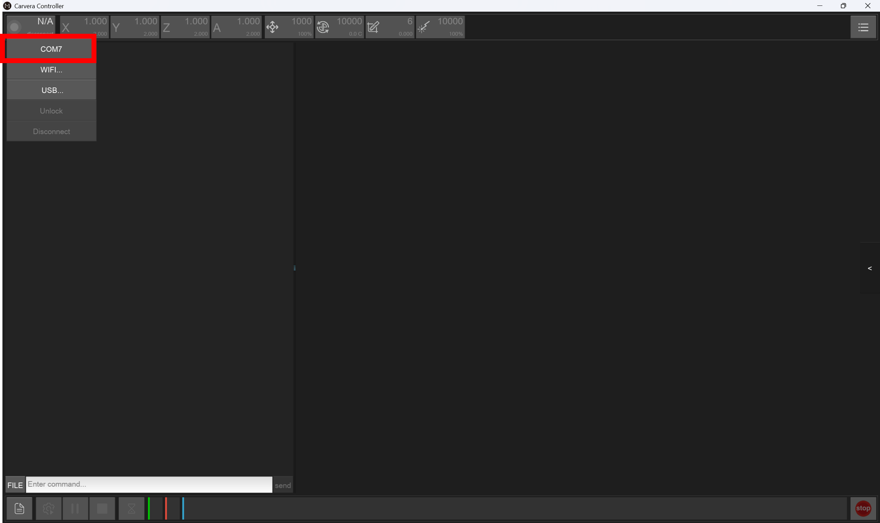
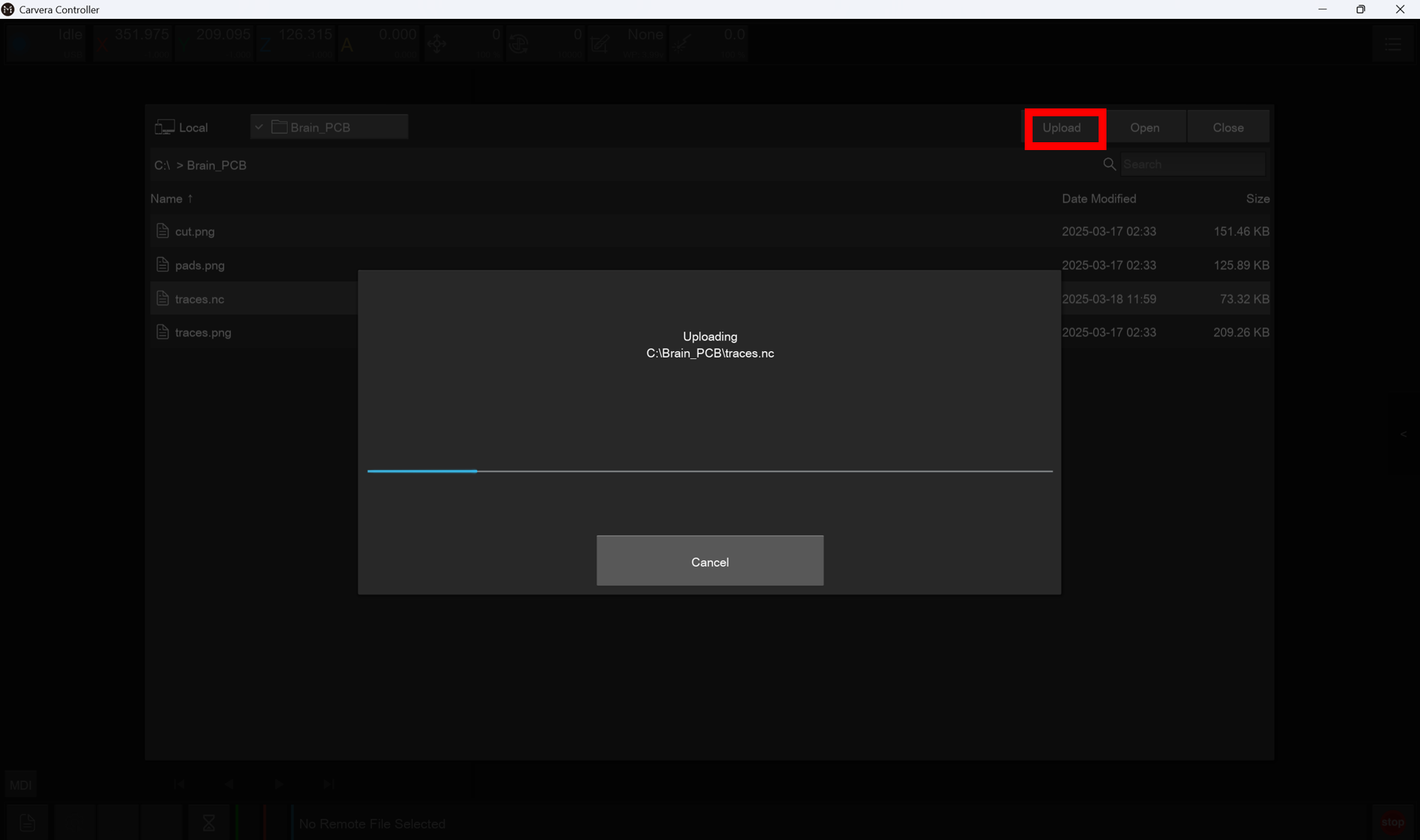
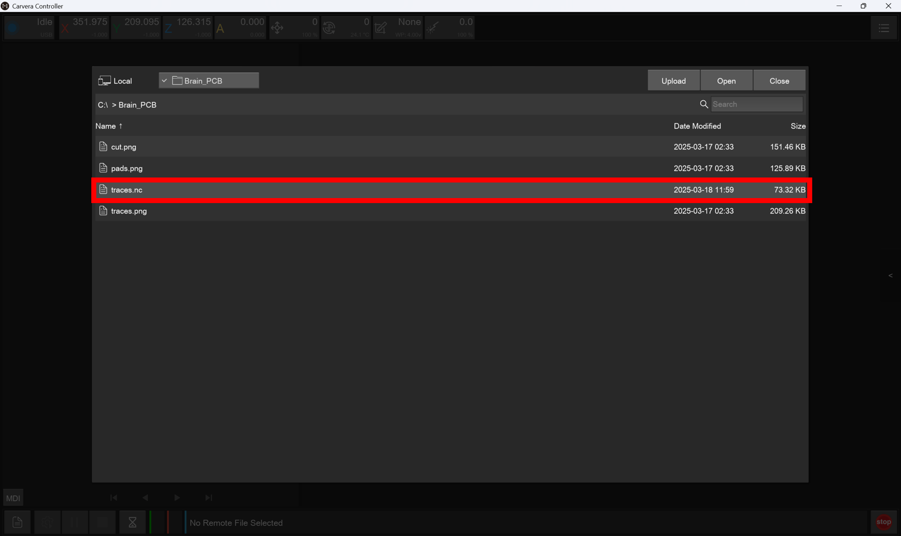
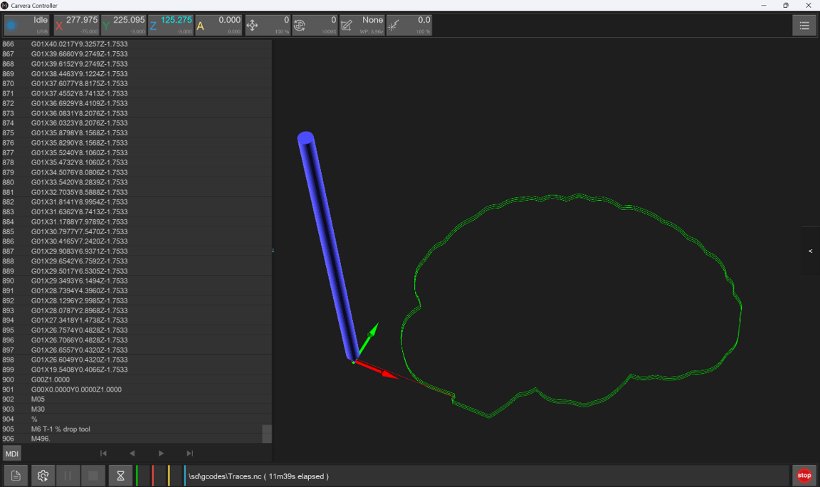
I opened Carvera Controller, connected to 📁 COM7 (the COM port depends on your laptop/PC), and loaded the toolpath files generated by ModsProject into the machine's local memory.
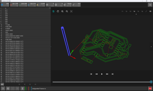
2. Setting the Origin Point
I set the origin point, avoiding (0,0) to prevent interference with the screws. Instead, I placed it at (7,7) for safety.
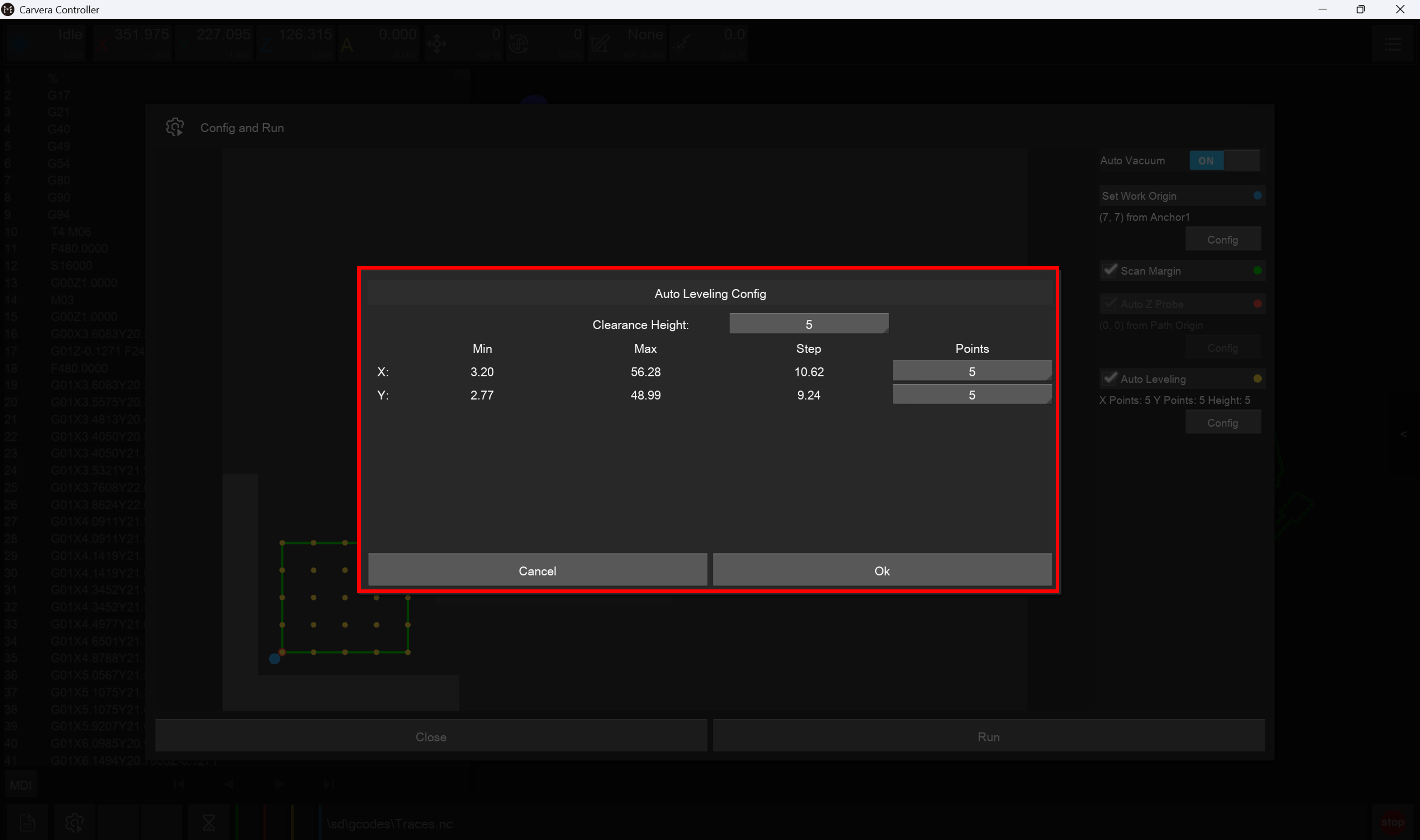
3. Scan Margin & Autoleveling
I activated Scan Margin and enabled Autoleveling with 5 points.
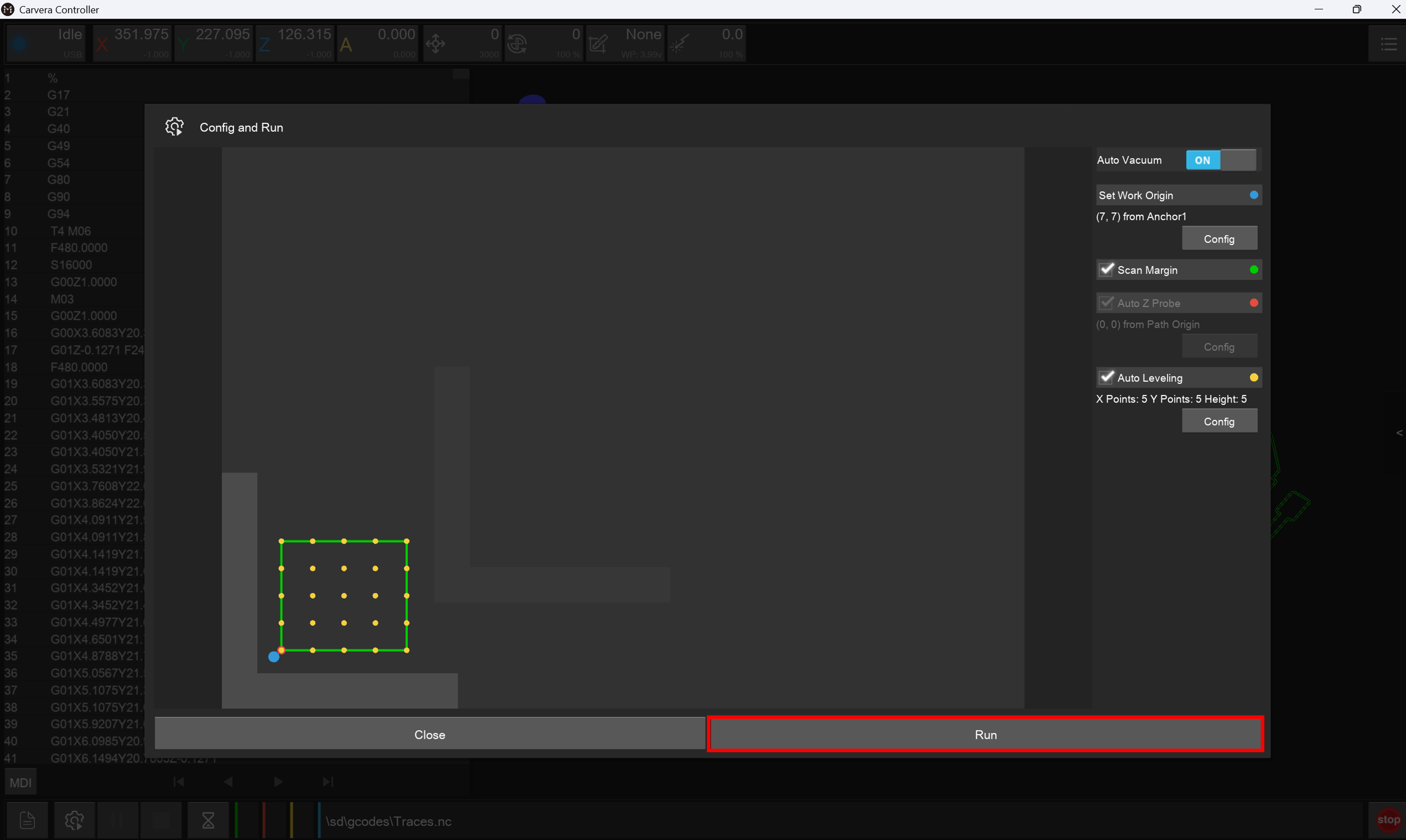
4. Milling the Traces
I ran the milling process for the traces.
External Cut
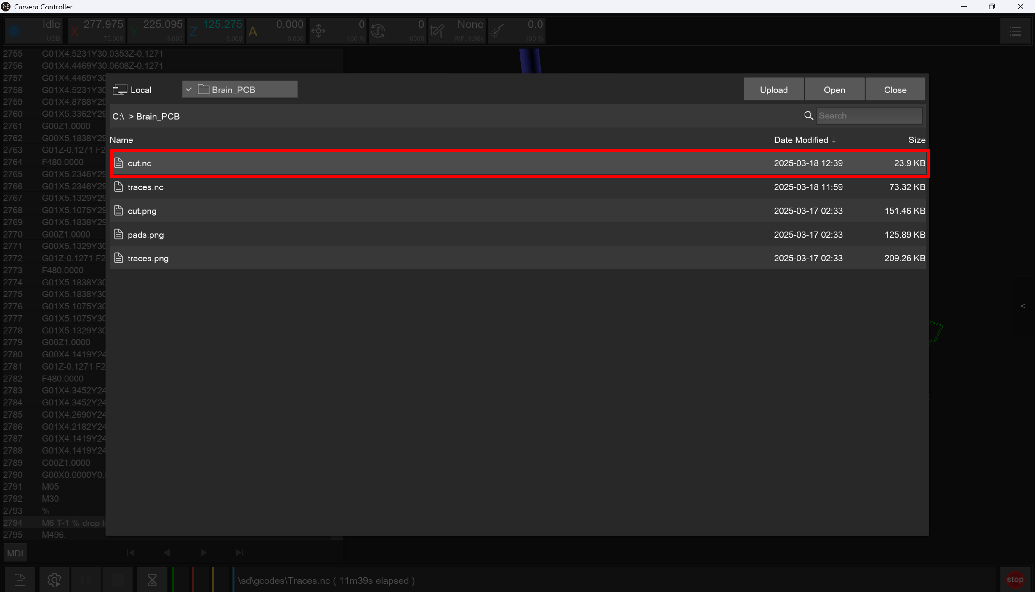
1. Opening & Loading the File
I followed the same steps to open and load the cutting toolpath file.
2. Recalibration
According to the manual, recalibration wasn't necessary since the machine had already been calibrated. However, based on a previous experience, I chose to recalibrate with the same settings:
- In an earlier attempt, skipping recalibration caused the tool to break. 😞
- To ensure precision and avoid damage, I recalibrated before proceeding.
3. Milling the Board Outline
I ran the milling process for the Outline Cut.
Milling Process
1. Before Hitting Run
Before hitting 🖰 Run, I ensured that the material was in the correct position and properly secured. I also checked that the tools were in their correct positions: Tool #4 for the traces and Tool #3 for the external cut.
Secured board
Tool #4
Tool #3
Traces
2. Starting the Milling
I started milling the traces.
- Carvera first performed the calibration based on my configuration in Carvera Controller.
- Then, it selected the tool.
- I carefully checked that the machine picked the correct tool — Tool #4 for traces.
3. Post-Milling Activities
- I monitored the milling process to ensure the machine was running correctly.
- I then removed the milling debris from the PCB surface using a vacuum.
- I then lightly sanded the board to remove rough edges and small copper burrs.
- I then inspected and cleaned the traces before continuing.
- I finally closed the lid of the Makera Carvera to prepare for the outline cut.
⚠️ Important — Safety Note: It's important to wear safety glasses while vacuuming, as tiny fiberglass particles from the board could get into the eyes.
External Cut
4. Milling the Board Outline
Then, I started milling the board outline.
- I verified that the machine selected the correct tool — Tool #3 for the cutting process.
- Once the milling was complete, I used a vacuum to remove any remaining material.
- I carefully removed the board from the machine.
- I lightly sanded the edges to smooth out any rough areas.
And with that, the Brain PCB board 🧠 was complete!
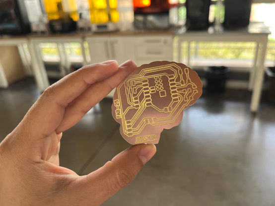
🛠️ Final Project PCB
The Brain Board was an important first step in understanding the complete PCB milling workflow. Fabricating it helped me become familiar with each stage of the process, identify possible issues early, and gain more confidence before working on the Final Project PCB. After finishing the Brain Board, the workflow felt much clearer and more organized for the next board.
With the experience from the Brain Board fresh in mind, I moved on to fabricating the Final Project PCB. The milling process followed the same workflow — preparing the copper blank, converting the Gerber files to PNG using Gerber2PNG, generating the toolpaths in ModsProject, loading the files into Carvera Controller, and running both the trace and outline cuts.
Stuffing & Soldering
With the board freshly milled, it was time for soldering. This was my first time working with components this small, so the process required much more precision and patience than the larger components I had soldered before.
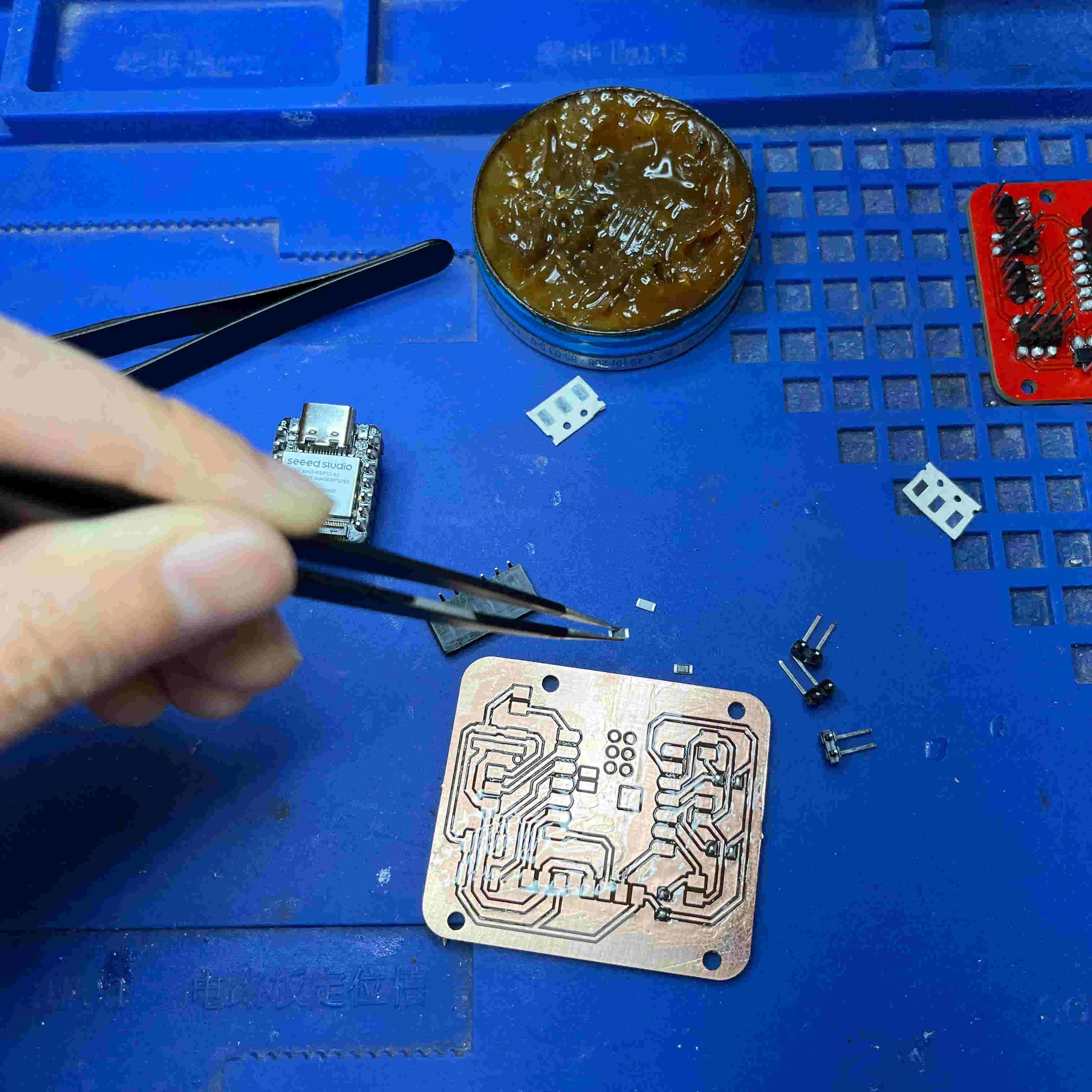
Before turning on the soldering iron, I first organized all the parts on the table. In total, the board used 14 SMD components, and laying everything out beforehand helped me clearly identify each part and make sure nothing was missing before starting.
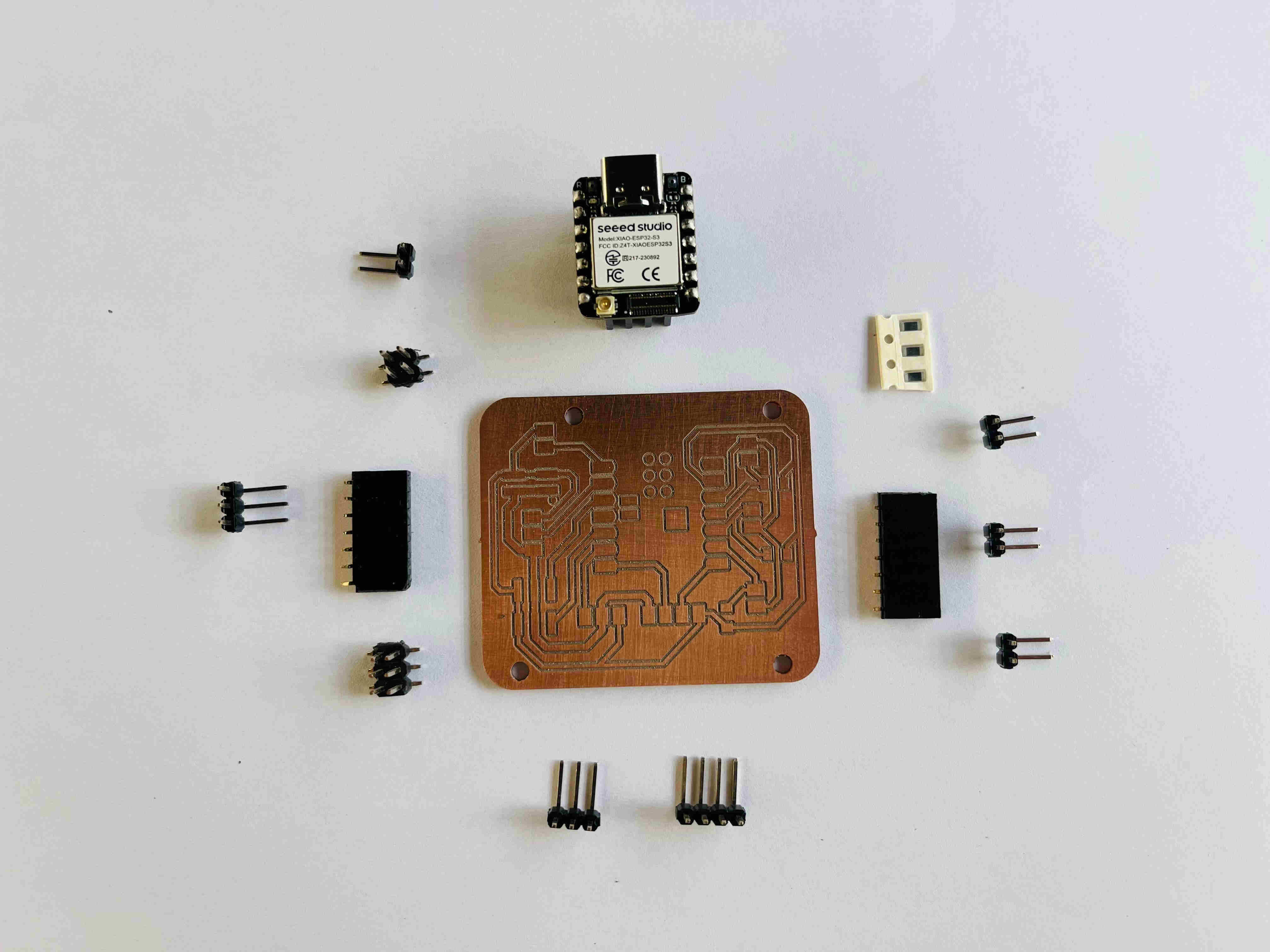
The Components
All 14 components on this board are SMD (Surface Mount Device), meaning they sit directly on the copper surface and are soldered in place without passing through the board. This keeps the design compact and clean.
| Component | Quantity |
|---|---|
| SMD Resistor 1kΩ | 3 |
| PinHeader 1x02 P2.54mm Vertical | 4 |
| PinHeader 1x03 P2.54mm Vertical | 2 |
| PinHeader 1x04 P2.54mm Vertical | 1 |
| PinHeader 2x02 P2.54mm Vertical | 1 |
| PinHeader 2x03 P2.54mm Vertical | 1 |
| PinSocket 1x07 P2.54mm Vertical | 2 |
| Total | 14 |
Soldering Workflow
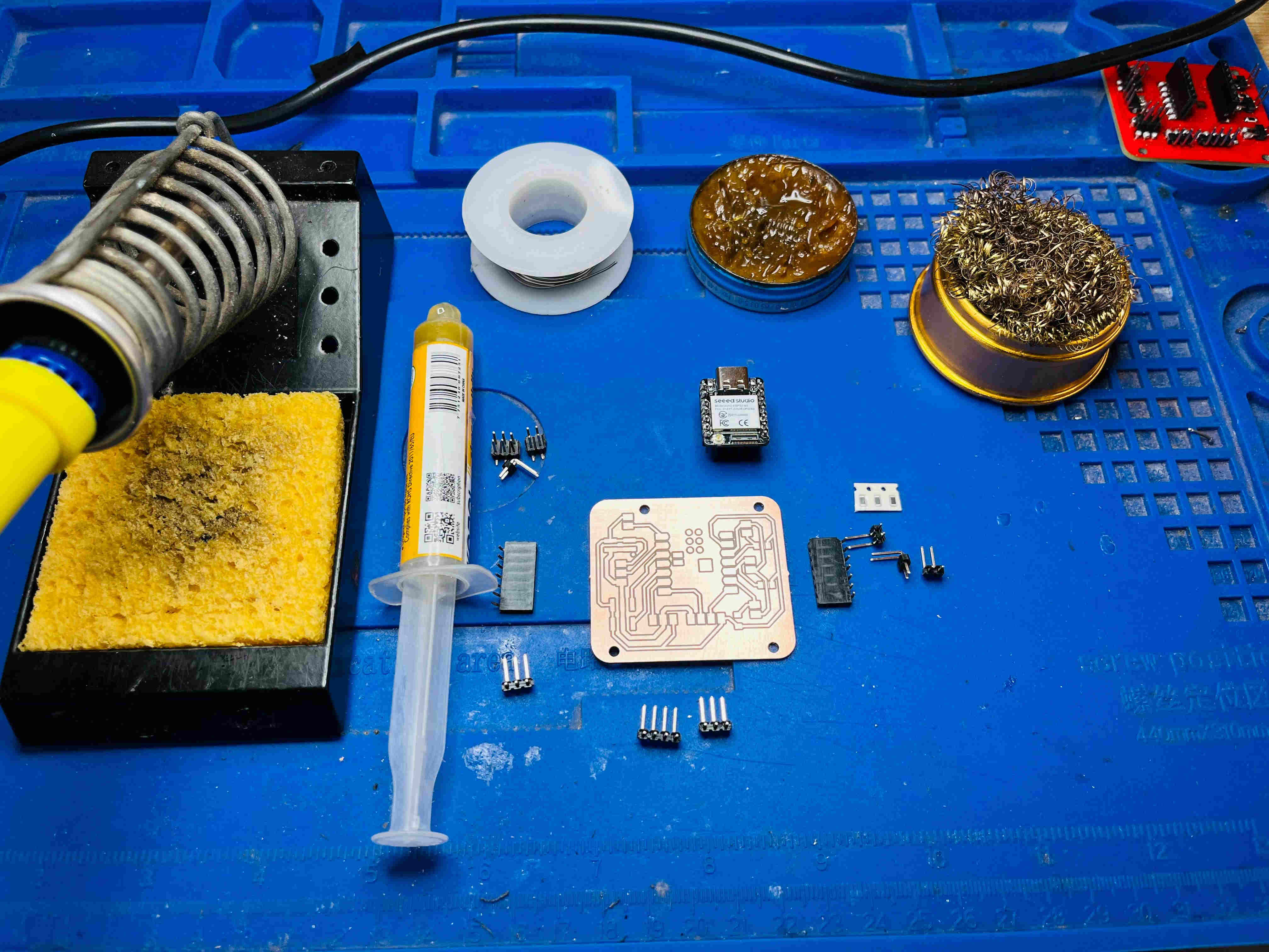
Step 1 — Setting Up the Workstation
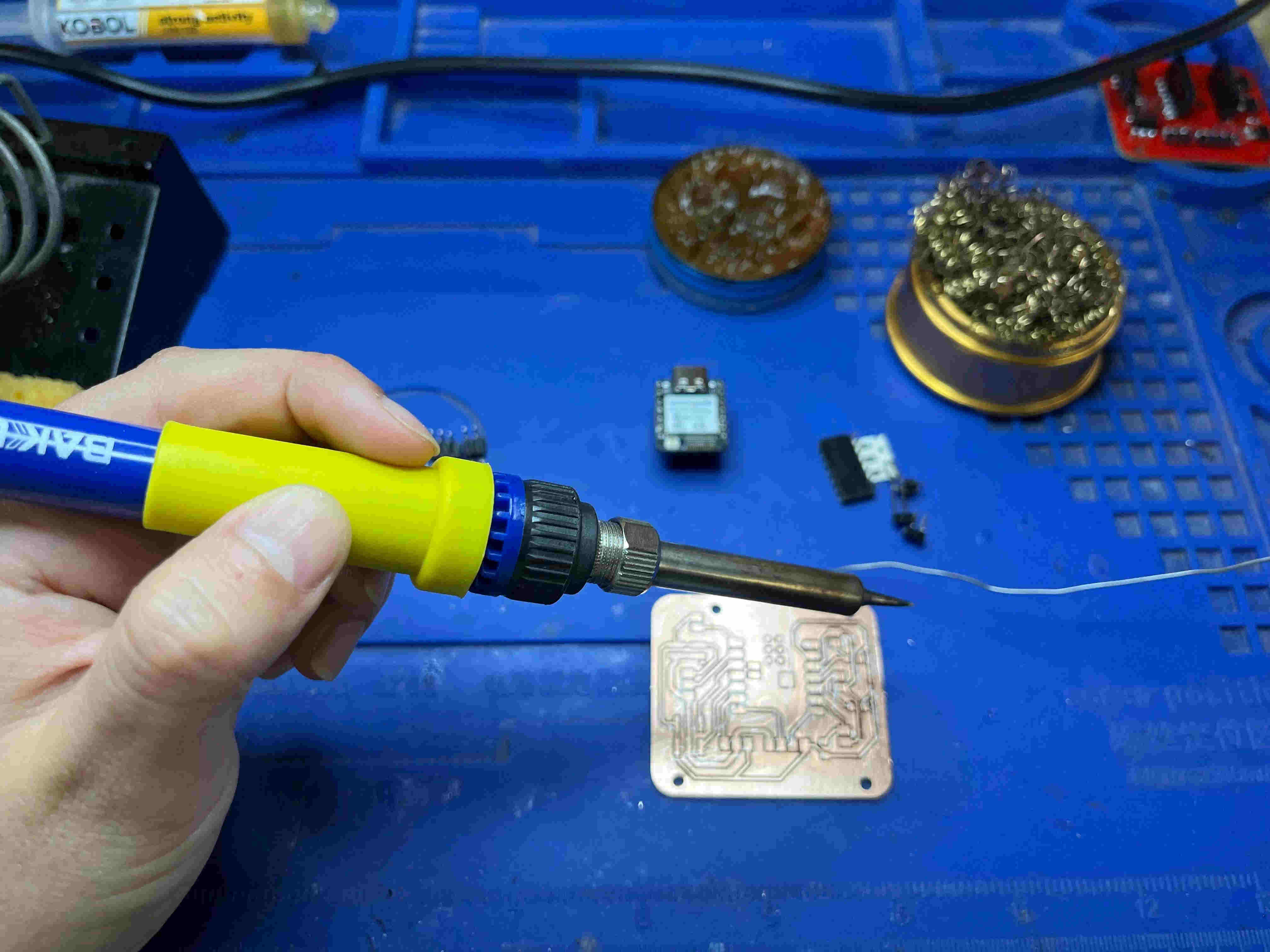
Before starting the soldering process, I organized all the necessary tools within reach: the soldering iron, solder wire, flux paste, a brass wire tip cleaner, and a damp sponge. Keeping the workstation clean and organized made the process easier, especially when working with small SMD components that require more precision.
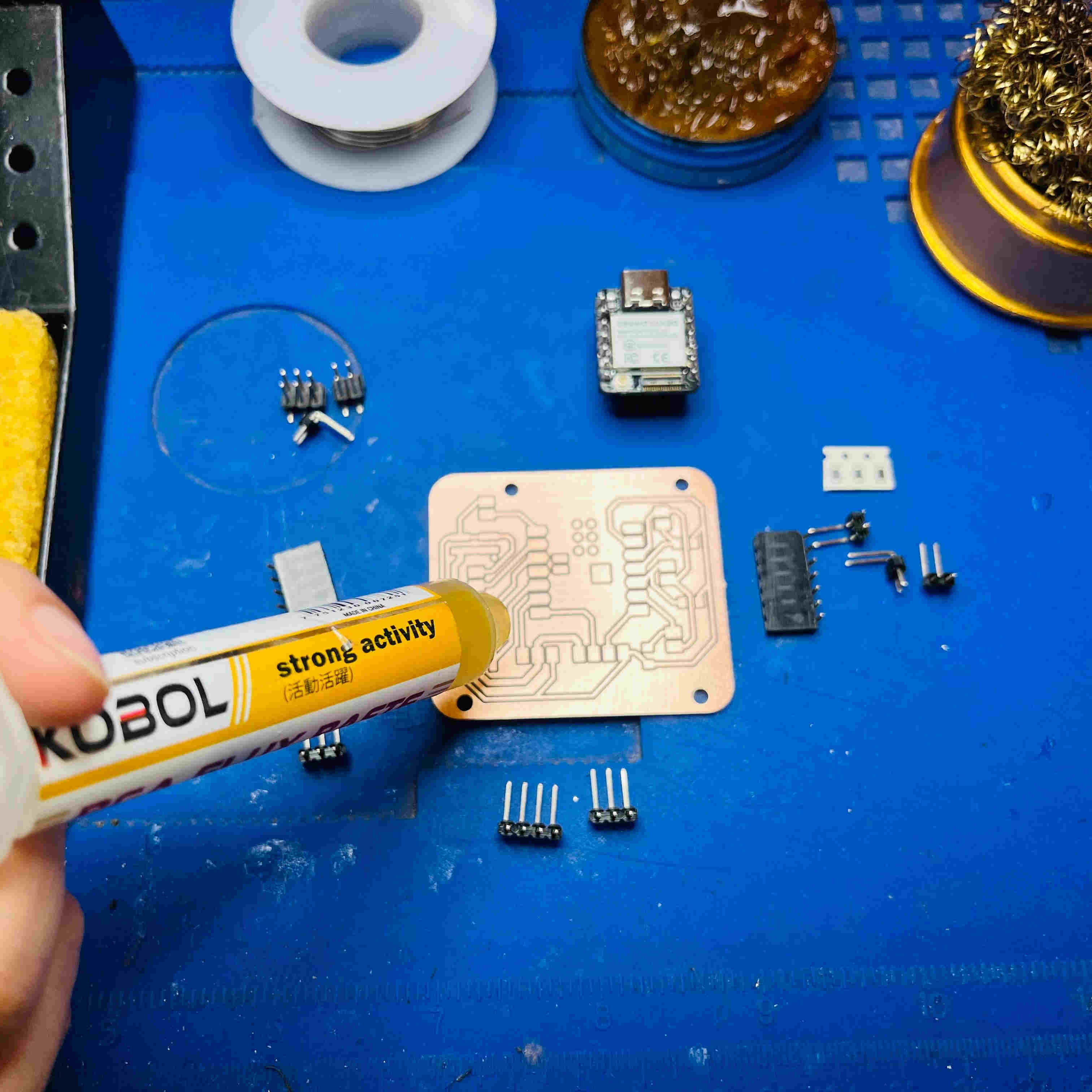
Step 2 — Applying Flux
One thing I learned very quickly is that flux makes the soldering process much easier. Before placing each component, I applied flux paste to the pads to improve solder flow and help the solder bond cleanly to the copper. It also reduced the chances of creating cold joints, which was especially helpful when working with small SMD components.
Step 3 — The Soldering Order
ones firstOne of the most important parts of stuffing a board is deciding the soldering order. I started with the smallest SMD components first and then continued outward from the center of the board. This made the process easier and prevented larger components from blocking access to smaller pads later on.
| Order | Component | Why |
|---|---|---|
| 1st | SMD Resistors (1kΩ) | Smallest and most delicate — need clear access |
| 2nd | SMD Pin Headers (2x02, 2x03, PinSocket 1x07) | Mid-size, still need precision |
| 3rd | Remaining Pin Headers (1x02, 1x03, 1x04) | Larger, easier to handle, soldered last |
💡 For the SMD components I used tweezers to position each part carefully on the pad before bringing the iron close. A steady hand and a bit of patience go a long way here.
⚠️ Problems & How I Fixed Them
Not every solder joint went perfectly, especially while working with small SMD components for the first time. These were some of the issues I encountered during the process and how I solved them:
| Problem | What happened | How I fixed it |
|---|---|---|
| Solder bridges | On a couple of pads, solder flowed between adjacent pins creating an unintended connection | Used a desoldering pump to cleanly remove the excess, then re-soldered the joint properly |
| Solder splatter | Tiny solder droplets splattered onto the board near the smaller components | Inspected every trace carefully — fortunately none of the splatter damaged any trace, so no further action was needed |
| Pace | Being out of practice, the whole process took longer than expected | Chose to slow down deliberately — better to take the time and do it right than to rush and damage a trace or lift a pad |
🎉 The good news: no pads lifted, no traces were damaged, and every joint ended up solid. Slowing down and using flux throughout made all the difference.
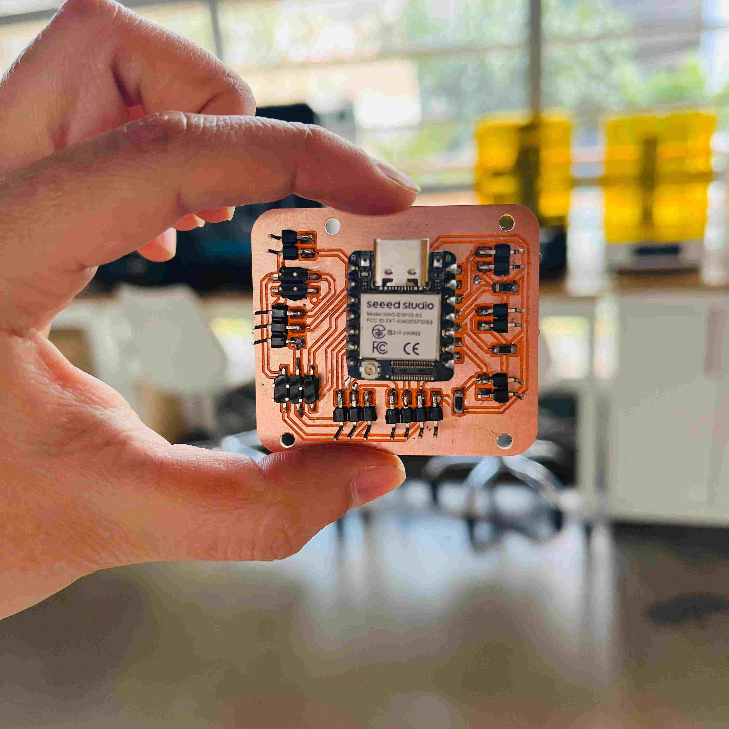
And with that — the Final Project PCB was fully assembled! 🎉 Seeing all those components in place, knowing every joint was done by hand, felt genuinely rewarding. It's one of those moments where the work suddenly feels very real.
💡 Functional Test
The PCB includes dedicated pin headers for two main connections: one for the Seeed Studio XIAO ESP32S3 module and another for the external 5V power supply. Keeping these connections separated makes the system easier to power, test, and replace when needed.
For the test, I connected a 16-LED NeoPixel ring to the board using female-to-female Dupont cables for signal, 5V, and GND. The external 5V connection was necessary because the LED ring requires a dedicated 5V supply to operate correctly.
⌨️ The Code
The test program was written in Arduino IDE using the Adafruit NeoPixel library. The code sequentially turns on each LED of the 16-LED NeoPixel ring with white light until the entire ring is illuminated. The animation then repeats continuously in a loop.
Final Thought
As part of the 2025 cycle, I fabricated the first version of the PCB (Brain Board 🧠) that I had designed as an initial test, which helped validate its basic functionality and identify improvements for the final design. In 2026, I fabricated the new version of the board and carried out the corresponding tests. It worked on the first try: the NeoPixel ring lit up correctly, confirming proper fabrication, solid soldering, and correct communication with the Seeed Studio XIAO ESP32S3. In addition, I also fabricated and tested a second PCB for the robot accessory, which worked as expected. 🥳