W6 | Electronics Design
📝 Group Assignment:
- Use the test equipment in your lab to observe the operation of a microcontroller circuit board (as a minimum, you should demonstrate the use of a logic analyzer).
- Document your work on the group work page and reflect what you learned on your individual page.
What is a Logic Analyzer?
A logic analyzer is an instrument that captures and displays digital signals across multiple channels simultaneously. Unlike an oscilloscope, which shows the shape of a signal, a logic analyzer focuses on timing and logic states—whether a signal is HIGH or LOW at a given moment. This makes it particularly useful for analyzing digital communication protocols such as UART, I2C, and SPI.
How We Used It
For this group assignment, we connected an 8-channel USB logic analyzer to a XIAO RP2040 board. The board was programmed to generate a digital pulse on pin D0 and transmit a serial message through pin D1. Using PulseView, we captured both signals and added a UART protocol decoder to interpret the transmitted data.
What Caught My Attention
This was my first time using a logic analyzer, and what caught my attention most was seeing a readable message—"FabAcademy 2026"—represented as a sequence of digital bits traveling through the signal line. Understanding that digital communication is based on 0s and 1s is one thing, but seeing those bits captured, timed, and decoded from an actual signal made the concept much clearer.
To see the full process in detail — including the wiring, Arduino code, PulseView configuration, and signal capture — you can visit the following page here.
What I learned?
I learned that a logic analyzer is not only useful for verifying that a signal exists, but also for observing and analyzing communication between devices. Being able to capture, time, and decode signals makes it possible to identify whether a message was transmitted correctly, whether data became corrupted, or whether communication timing is incorrect. This experience gave me a much clearer understanding of how digital communication protocols work and how they can be analyzed and debugged in practice.

📝 Individual Assignment:
- Use an EDA tool to design a development board that uses parts from the inventory to interact and communicate with an embedded microcontroller.
Designing My Microcontroller Development Board
BRAIN BOARD 🧠
Pre-design Stage
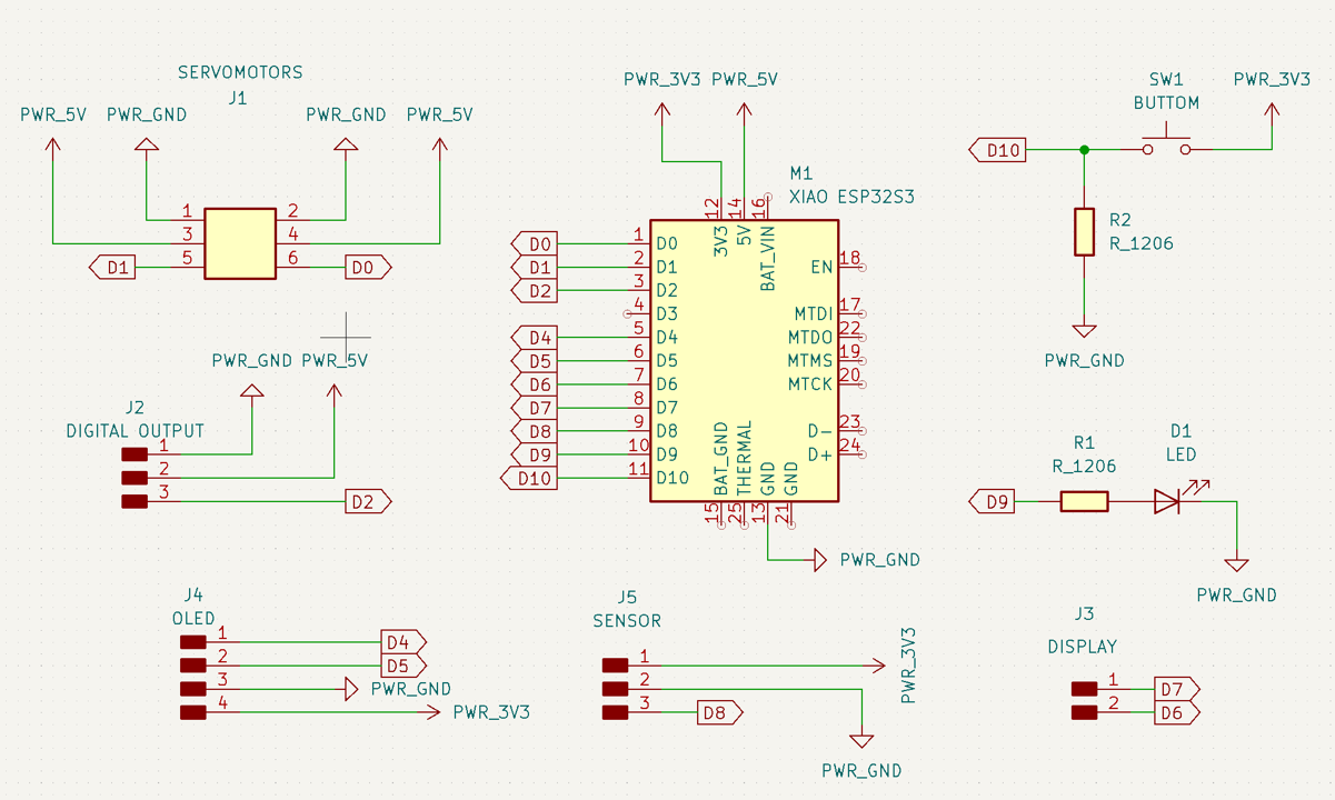
For this week, we had to use an EDA tool to design a PCB that communicates with a microcontroller. Jorge and I decided to use this task as an opportunity to design the PCB for the microcontroller that will be used in my final project. So... I began by identifying the core functions that my project will perform and then determining the necessary components that the PCB should have — both inputs and outputs — to make sure the system works as intended.
We started with a fun brainstorming session to decide which inputs and outputs my main board should include. It was exciting to imagine how each component would interact as part of my final project. After several ideas, we decided to include the following components:
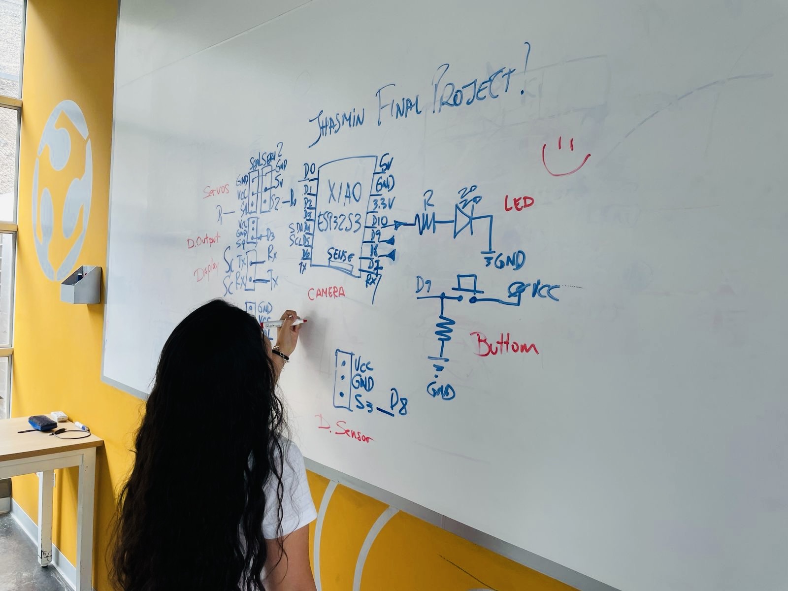
🔹 Outputs
Two servo motors (to control the robot's arms), one Digital Output (for an external actuator or similar), a Display connected through RX and TX, an OLED Screen using the SDA and SCL pins (as an alternative if the main display isn't available), and one LED as a visual indicator during the testing phase.
🔸 Inputs
One Digital Sensor (such as a PIR or obstacle sensor), and one Push Button for testing.
And before jumping into the PCB design using the EDA tool, I needed to understand how the microcontroller connects to each part. This meant checking the function of every pin, identifying which ones provide power (VCC), which ones are for ground (GND), and which pins can send or receive data. I also verified the voltage levels that each device uses — some components work with 3.3 volts, while others require 5 volts.
In the following image, you can see the result of this planning process, where I mapped out each connection before starting the PCB design.
⚙️ Setup Stage

For the design stage, I used KiCad EDA, an open-source tool widely used for electronic design. One of its greatest advantages is that it combines schematic capture, PCB layout, and even 3D visualization of the board within the same environment. It's intuitive, flexible, and completely free, which makes it perfect for learning and professional projects alike. You can download the program from the following link according to the type of computer you have.
Setting Up the Fab Academy Libraries in KiCad:
Before starting the PCB design, it was necessary to configure the official Fab Academy libraries in KiCad. These libraries contain all the standardized electronic components used in Fab Labs around the world, ensuring that every PCB we design can be easily reproduced anywhere.
1. Downloading the libraries
The first step was to download the folder 📁 kicad-master from the official repository: Fab Lab - KiCad Repository. This folder includes everything needed for PCB design in KiCad:
📁 fab.kicad_sym— the symbol library📁 fab.pretty— the footprint library📁 fab.3dshapesand📁 fab.3dsource— optional 3D models
2. Adding the Symbol Library
I opened KiCad and went to 🌐 Preferences → Manage Symbol Libraries. In that window, I clicked 🖰 + and added the file 📁 fab.kicad_sym.
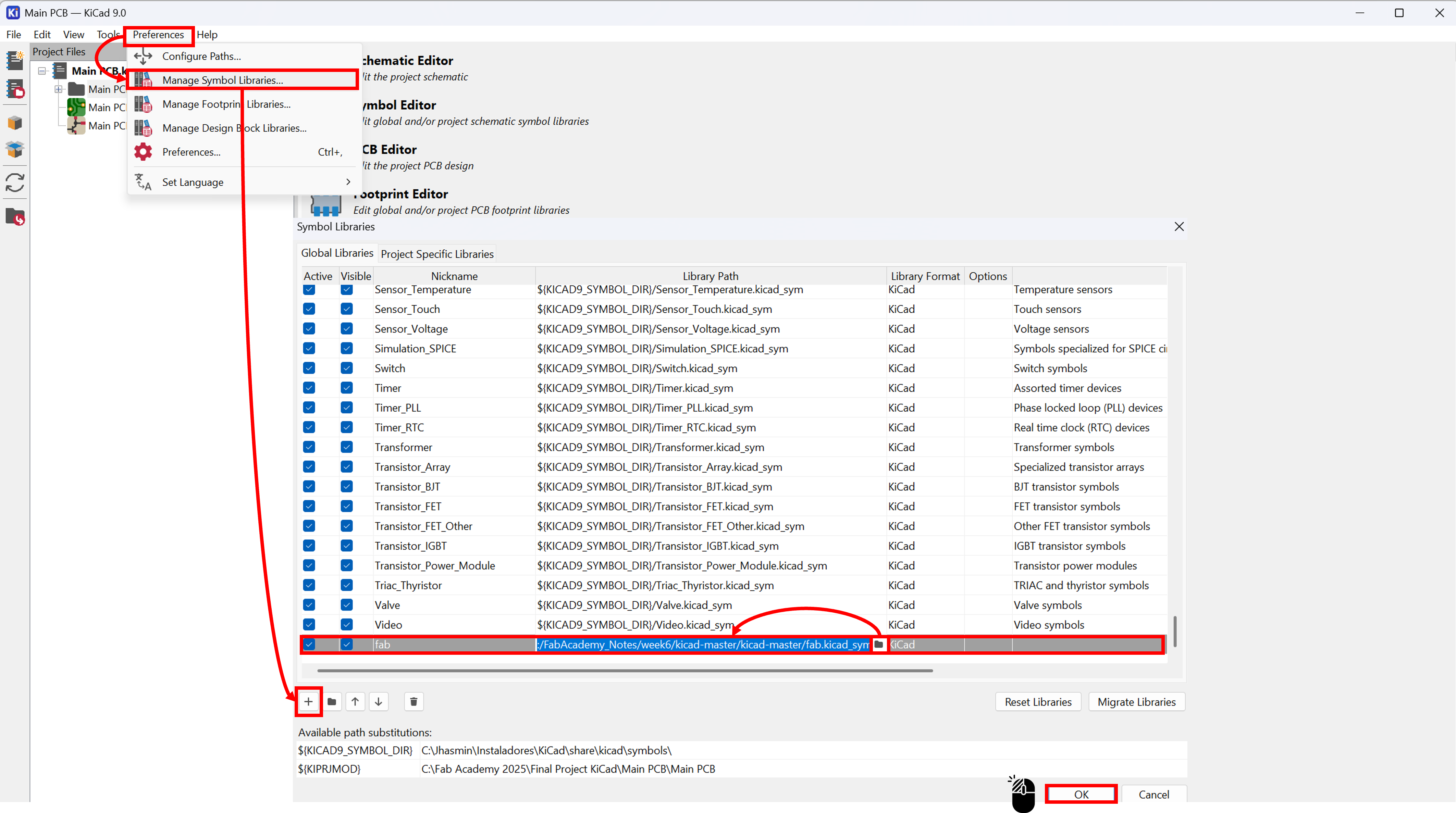
📝 Note: This library allows me to access all Fab Academy standardized symbols directly from the Schematic Editor, making it easier to design circuits.
3. Adding the Footprint Library
I went to 🌐 Preferences → Manage Footprint Libraries and added the folder 📁 fab.pretty.

📝 Note: This step connects each schematic symbol with its corresponding physical footprint, so that KiCad knows exactly how each component will appear and be positioned on the PCB.
4. Verifying the configuration
Once both libraries were added, I verified that KiCad correctly listed them in the Global Libraries section. From this point on, I could select and place Fab components both in the schematic and PCB layouts.
📝 Design Stage
Once the Fab libraries were added, I began creating the schematic in KiCad's Schematic Editor. The first step was to place all the necessary components for my project — including the microcontroller, connectors for the servomotors, sensor, display, digital output, OLED, LED, and button. All these components were taken directly from the Fab library, which I had previously added during the setup stage.
To make the schematic more organized and easier to read, I used Global labels instead of connecting wires directly between components. Those symbols allow the same signal name to be shared across different parts of the schematic, which keeps the design cleaner and prevents overlapping lines. For example, power and ground lines such as PWR_5V, PWR_3V3 and PWR_GND were defined once throughout the entire circuit.
📝 Note: While creating the schematic, I used several basic tools and symbols available in KiCad. Here are three of the most important ones and their purpose:
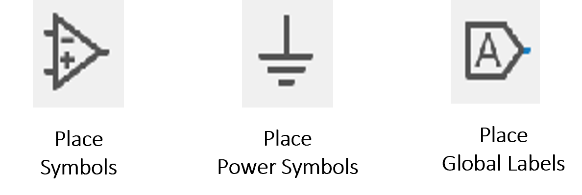
- Place Symbols — used to add symbols from the library to your schematic. It's the tool to insert new components into your design.
- Place Power Symbols — provides different voltage options that help define the electrical connections in your schematic.
- Place Global Labels — allows you to name a connection so that it links automatically to other parts of the schematic, even if the wires are not physically drawn together.
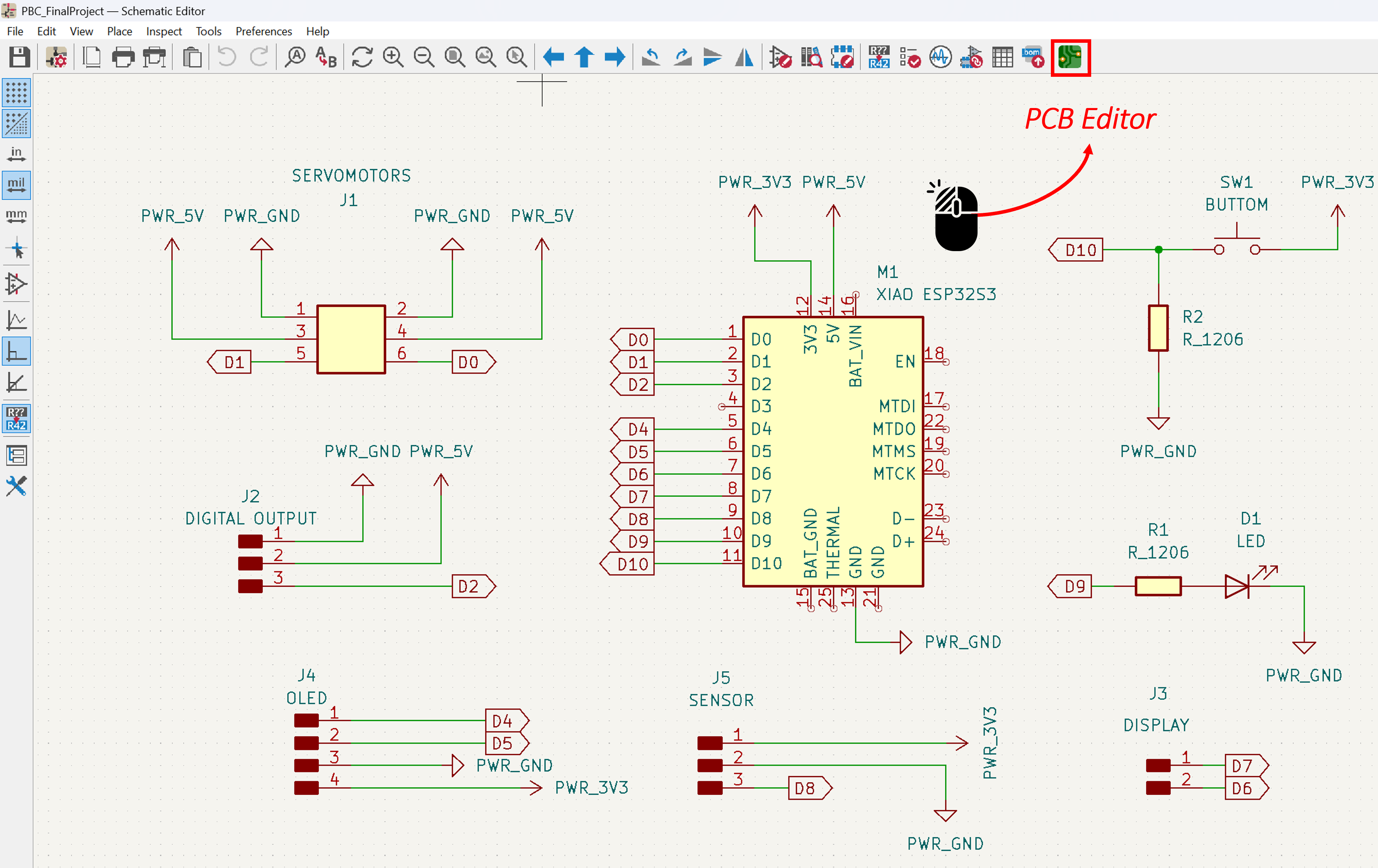
🔌 Schematic Design
After adding all the components to the schematic, I began connecting them using power symbols and global labels to organize everything clearly. Little by little, the circuit started to take shape, and I could see how each part connected to the XIAO ESP32S3. To indicate the power sources, I used the symbols from the Fab library — such as PWR_3V3, PWR_5V and PWR_GND — so it would be easy to recognize which components worked at 3.3V and which ones needed 5V.
Using global labels helped me avoid having too many crossing wires on the screen, keeping the design clean and easy to follow. Once everything was labeled and connected, I reviewed the schematic to make sure that each pin matched its correct signal and power line. Seeing the complete schematic ready was a very satisfying step before moving on to the PCB design stage.
🔌 PCB Editor
After finishing the schematic, I opened the PCB Editor from KiCad's main menu to start designing the physical board. The first step was to update the PCB from the schematic, using the option found in the Tools menu. This automatically loaded all the components and their connections onto the board workspace.
Before starting the routing, I configured some important parameters in the Board Setup menu. I defined the trace widths, setting 0.4 mm for signal lines and 0.8 mm for the ground traces, since they need to handle higher current. I also adjusted the design constraints, setting the clearance to 0.4 mm — this is essential to avoid spacing errors and ensure that the dimensions don't exceed the milling tool's diameter.
1. Bring in the schematic
In PCB Editor go to 🌐 Tools → Update PCB from Schematic.

2. Configure board rules (Board Setup):
Pre-defined Sizes:
In the Board Setup window, under the Design Rules section, I customized the trace settings for my board. I created two custom trace widths:
- 0.40 mm for the signal traces (standard connections)
- 0.8 mm for the power traces, since they carry more current

Constraints:
I configured the Design Constraints to define the spacing and manufacturing limits of my PCB. I set a clearance of 0.40 mm — especially important when milling the board, since the tool's diameter must fit between tracks without removing unwanted material.

3. Starting the Routing Process
Once all the design rules were set, I began the routing process — the stage where every electrical connection from the schematic is physically drawn on the PCB. For this design, I used a trace width of 0.4 mm for all routes, keeping the layout simple and consistent. While routing, I made sure to avoid 90-degree angles in the traces. Instead, I used 45-degree corners, which help the current flow more smoothly and reduce electromagnetic interference.
As I started connecting the components, I noticed that some traces were crossing each other, which made the layout look messy and difficult to route properly. To fix this, I began reassigning pin connections and rearranging component positions until I found a cleaner and more efficient layout.

📝 Note: In the end, the routing looked well-organized, with smooth connections and enough spacing to ensure a functional and visually clear design.
4. Designing the Board Shape (Edge.Cuts)
For this stage, I wanted my PCB to have a more creative and meaningful shape — not just a simple rectangle. Since this board will hold the microcontroller that represents the "brain" of my little robot, I decided to design it in the shape of a brain. 🧠
To start, I measured the approximate size of the board based on the components' arrangement and space needed for connections. Then, I created the 2D outline in CorelDRAW, carefully sketching the curves to give it an organic look while keeping it functional for fabrication. Once the design was ready, I exported it in DXF format, so I could import it directly into KiCad's Edge.Cuts layer. To do this, I followed these steps:
- Opened the file through
🌐 File → Import → Graphics - Adjusted the scale and set the default line width to 0.2 mm
- Made sure to select the correct layer: Edge.Cuts, since this layer defines the actual border of the PCB during manufacturing.
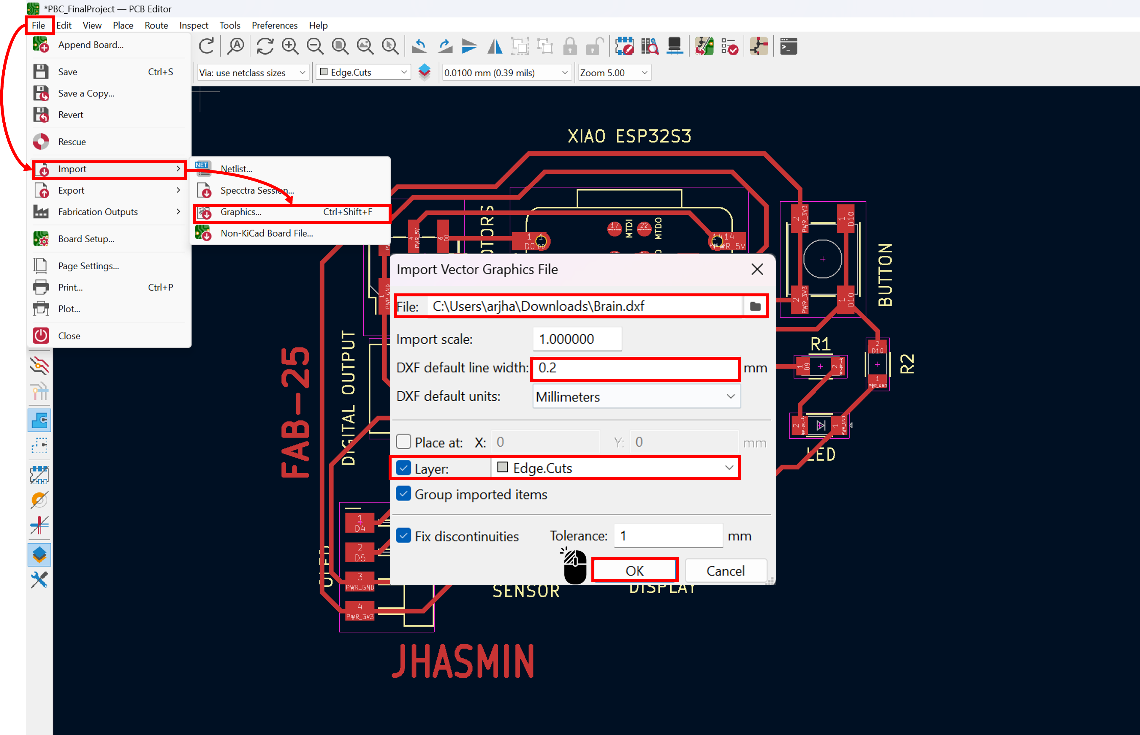
📝 Note: After importing, I checked that the contour fit properly with the components' layout.
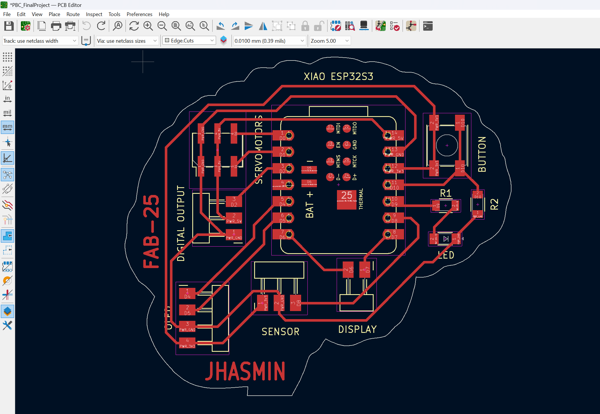
5. Checking Design Rules (DRC)
Once the board outline and routing were complete, the next important step was to run the Design Rule Check (DRC). This tool helps detect any electrical or geometric errors that might cause problems during manufacturing — such as unconnected nets, overlapping traces, or components placed too close to the board edges.
In KiCad, I opened the DRC panel from the 🌐 Inspect → Design Rules Checker menu.
📝 Note: After running the check, the software automatically highlighted a few small issues — mostly traces that were too close or slightly misaligned pads. I carefully reviewed and corrected each one until the message "No errors found" finally appeared on the screen ✅.

6. 3D Viewer — Visualizing the Final Board
With the routing completed and all design rules checked, I opened KiCad's 3D Viewer to see how the board would look in its final form. The 3D Viewer is a powerful tool because it allows you to visualize the PCB with all its components in three dimensions, giving a much more realistic idea of spacing, orientation, and assembly.
When the viewer loads, KiCad automatically replaces each footprint with its corresponding 3D model. Most Fab Academy components already include compatible 3D models, but sometimes a specific part may not be available. In those cases, it is possible to add your own:
- Download or create a STEP (.step) 3D model of the component.
- Place the file inside the
📁 fab.3dshapesfolder. - In the footprint editor, link that STEP file to the corresponding footprint.
📝 Note: Once linked, the component will appear correctly in the 3D Viewer as part of your board.
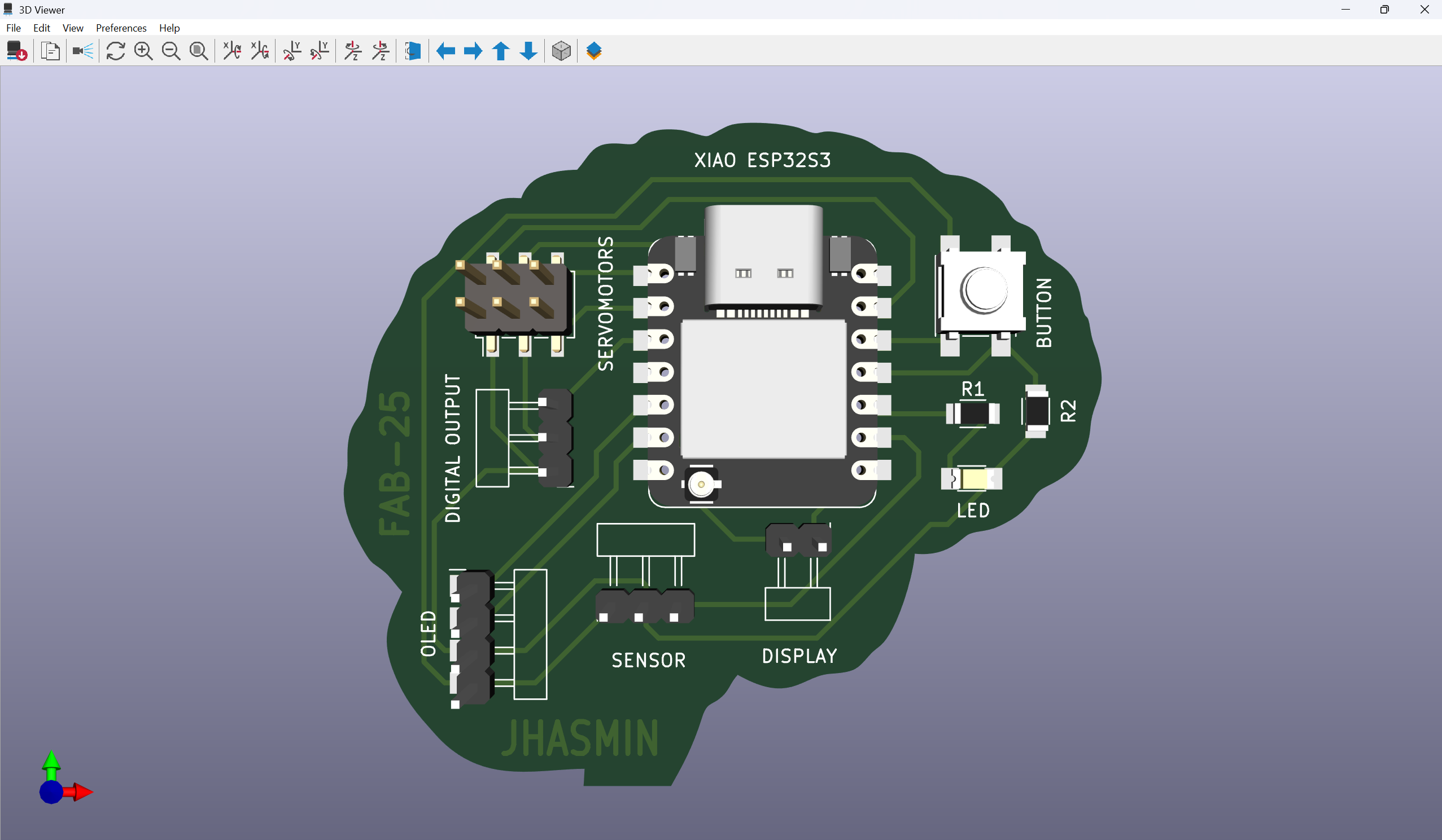
KiCad's 3D Viewer
Final Project PCB Design
This board represents the evolution of the design started earlier in the course. As the robot project became more defined, it became clear that the first version needed to be updated to better match what the robot actually needs — new components, new connections, and better design decisions. The design process followed the same workflow described above: schematic in KiCad, component placement, routing, DRC, and 3D view.
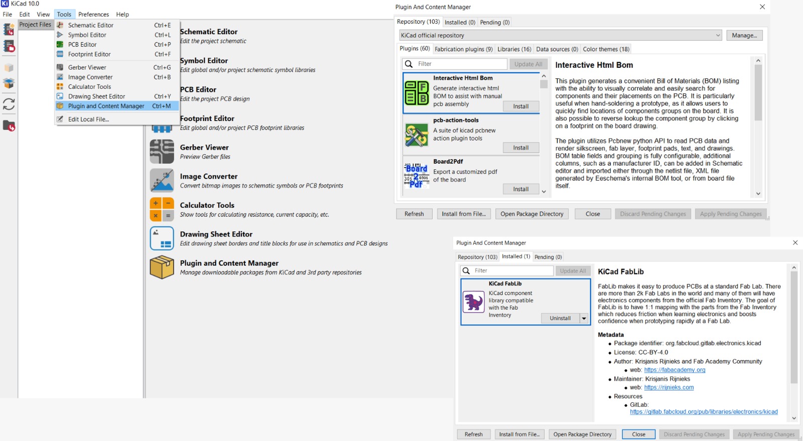
⚙️ Setting Up the Libraries
For this new version, the component libraries were already configured from the previous design, so most of the work could continue without interruption. However, during the process a KiCad update was available along with a newer version of the KiCad FabLib. To make sure everything was compatible and up to date, the library was reinstalled following these steps.
FabLib is now available as an official KiCad plugin, which means manual installation is no longer required. It can be accessed through its official repository:
FabLib.
The KiCad FabLib file can be found at the official repository: gitlab.fabcloud.org. To install it from file, the following steps were followed:
- Go to
🌐 Tools → Plugin and Content Manageror press🖰 Ctrl + M - Click
🖰 Install from File... - Look for the
📁 kicad-fablibzip file - Click
🖰 Open
What Changed and Why
This is not a completely new design — it is an evolution of the first version. Both were designed for the same robot, but as the project became clearer, the components and decisions changed to better reflect the robot's final functionality.
| First Version | Final Version | |
|---|---|---|
| Microcontroller | XIAO ESP32S3 | XIAO ESP32S3 |
| Buttons | 1 (for testing) | 3 (happy, sad, angry) |
| LED | 1 individual LED | LED Ring |
| Sensor | Generic sensor | PIR Sensor |
| Sound | None | Buzzer |
| Display | OLED | New display connector |
| Extra output | Digital output | Removed |
| Power traces | 0.5mm | 0.8mm for 5V traces |
The first version was a starting point — it helped establish the KiCad workflow and validate the basic circuit. As the robot's design became more defined, each component was reconsidered. The single test button evolved into three buttons with specific emotional meanings. The indicator LED became a visible LED ring integrated into the robot itself. A PIR sensor was added so the robot can react to nearby presence instead of waiting for manual activation. The buzzer was incorporated to provide small sound cues and feedback, helping reinforce the robot's interactions. In addition, the trace widths were updated to follow better design practices for power distribution — using 0.8 mm traces for the 5V lines to safely support the higher current required by components such as the servomotors and LED ring.
🔌 The Schematic
The schematic was designed in KiCad connecting all components to the XIAO ESP32S3. Each peripheral has its own labeled connector, making it easy to identify, connect, and disconnect components during assembly and testing. Power is distributed through PWR_3V3 for logic components and PWR_5V for higher power components like the servomotors and LED ring.
PCB Layout & Routing
With the schematic complete, the components were arranged on the board keeping power and signal traces as separate as possible. One important decision during routing was using different trace widths depending on the type of signal:
- 0.4–0.5mm for signal traces (3.3V)
- 0.8mm for power traces (5V)
This is standard practice in PCB design — power traces need to be wider because they carry more current. If they were too thin, they could overheat or fail when components like the servomotors draw current.
Problems and Solutions
Designing a compact board where everything fits cleanly was one of the biggest challenges. Two specific problems came up during routing:
🔸 Traces too close together
When trying to keep the board small, some traces ended up too close to each other. This is a problem because traces that are too close can cause short circuits during fabrication. The solution was to rearrange some components and reroute the affected traces until there was enough clearance — the DRC helped identify exactly where the issues were.
🔹 Reordering pins for cleaner routing
Sometimes the logical pin order in the schematic — for example VCC, GND, OUT — created trace crossings on the board that were difficult to route cleanly. In those cases, the pin order in the connector was changed directly in the schematic — for example to OUT, GND, VCC — so that the traces could flow naturally without crossing each other. It required going back and forth between the schematic and the PCB layout, but the result was a much cleaner design.
🌟 Final Result
Once the routing was complete and all design rules passed, the 3D viewer was used to visualize how the final board would look. All connectors are clearly labeled and positioned around the XIAO ESP32S3, making the board easy to assemble.
The board was designed with a simple square shape intentionally. While the first version had a more creative brain-shaped outline, for this final version practicality took priority — a square board is much easier to mount inside the robot's structure. A complex shape would make it harder to fit, align, and secure the board in place, while a square can be positioned and fixed with minimal effort during assembly.
Final Thought
During the 2025 cycle, I designed my first PCB for the final project—a first attempt that helped me understand the basics of PCB design while also revealing areas for improvement. In 2026, I revisited the design with a clearer approach, focusing on better component placement and optimized routing, along with appropriate trace widths from the beginning. The result was a cleaner board designed specifically for the robot, with all design rules passing correctly and a layout optimized for easier assembly.