8. Electronic production
Group assignment:
- Characterize the design rules for your in-house PCB production process.
Submit a PCB design to a board house.
Individual assignment:
- Make and test a microcontroller development board that you designed.
- Extra credit: Make it with another process
Useful links
- KiCad homepage
- Carbide Copper homepage
- XTool homepage
- Wegstr homepage
- FabLab Akureyri - G-Code Modifier
- JLCPCB homepage
Group Assignment
How do I caracterize the design rules for my in-house PCB production.
Well, since I have to make my own board in the individual assignment, I will go through the process of making my own board. In week 6 I designed a control interface to use with Seeed.
It has screw connectors for all the pins on the Seeed by choice because I do not like loose connections, but it also has more connection points for 3,3V and ground for connecting external input and output devices.
I also included on the board two slide switches with NO and NC contacts and also four push buttons. The switches are powerd through the board with 3,3 volts so I only have to connect them to a input pin if I wish to use them.
So, in week six I finished drawing the schematic in KiCad, I also designed the PCB board so it should be ready for milling. I am going to use the CNC machine since the FabLab just recently got the XTool F1 Ultra Fiber laser
and since it can not do the holes I need in my board I would have to use the cnc machine anyhow to drill the holes.
The switches are from the electronics department at my school because there were no switches in FabLab inventory.
So the first thing is to plot the files from KiCad.
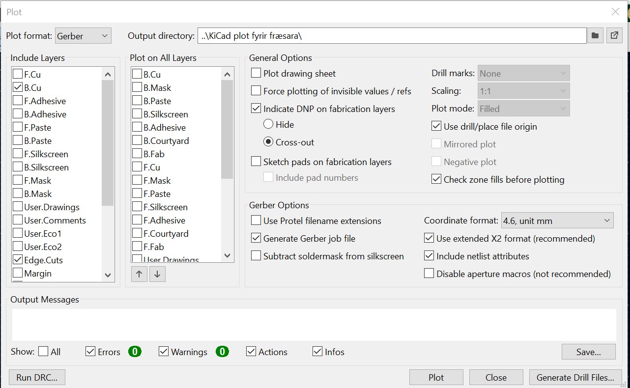
When ploting from KiCad I had to select the layers I wanted to use. Since this is only a single layer board, I only needed B.Cu and Edge Cut layers.
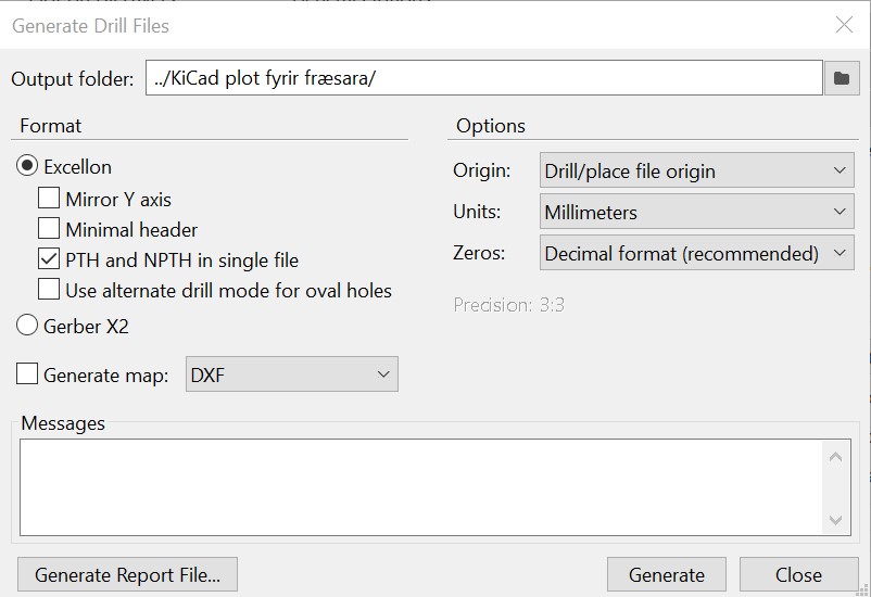
Then I needed to do the holes seperately and make a drill file.
For this project I am going to use Carbide Copper to convert .grb files to .nc files
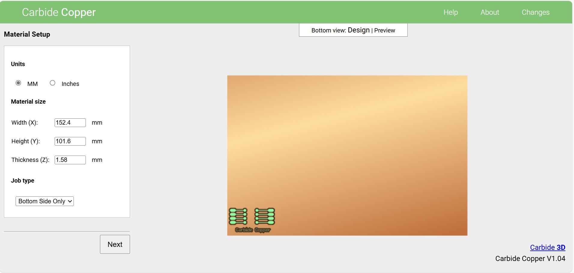
Copper Carbide is a web based converter, realy easy to use but not perfect. First I have to select board size and thickness.
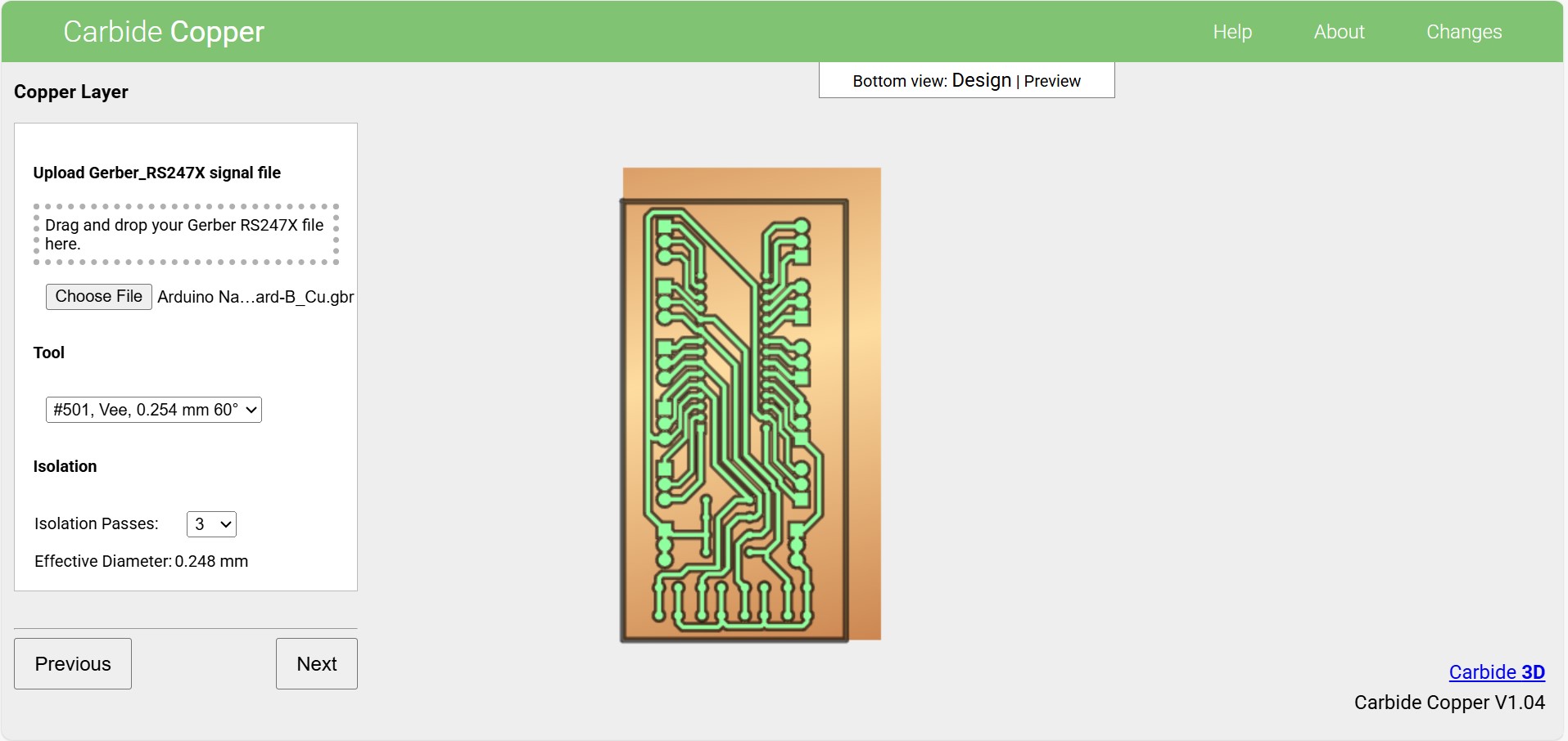
Then I have to select the B.Cu file I got from KiCad, and the circuit will appear on the board. It is very important not to forget the Drill/Place File Origin (the zero point) or the circuit will not end up on the board.
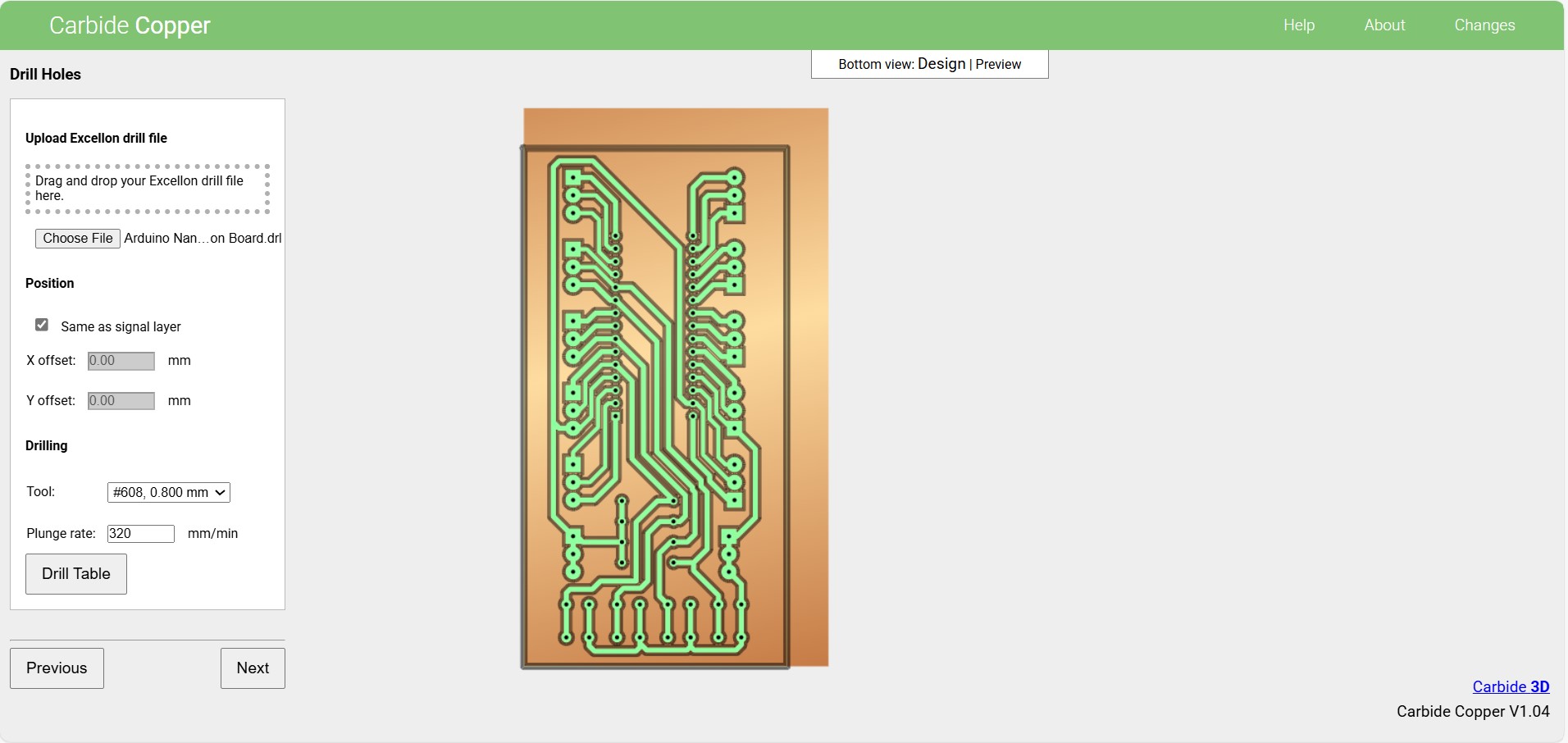
Then it is time for the holes. I dont have any mounting holes on this one so it is just the holes for the parts.
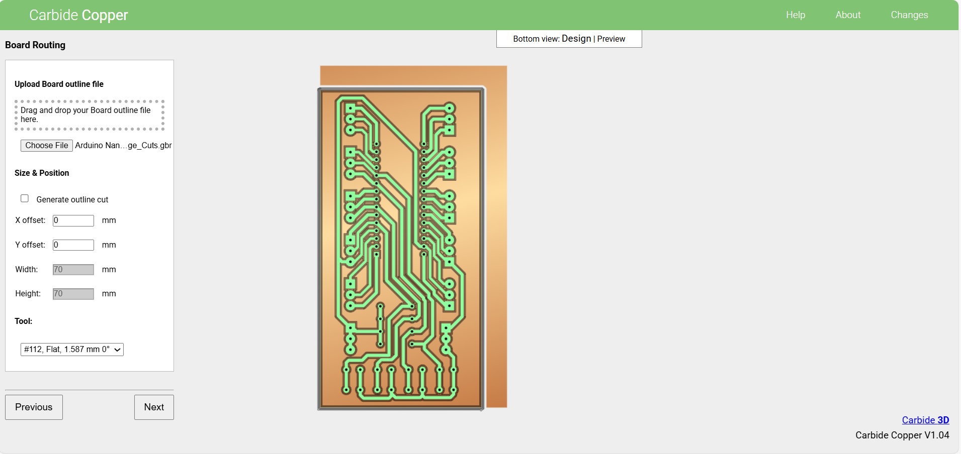
Then it is time to select the edge cut.
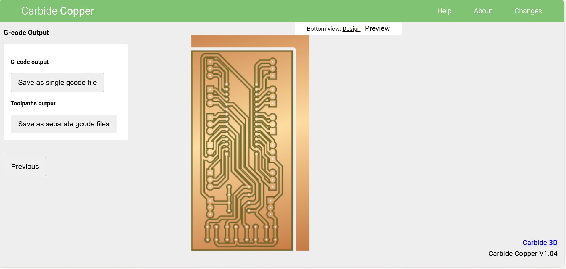
And finally, I had to save the different files separately as g-code for the cnc machine.
One of the down sides to Copper Carbide is that the edge cut is done in one pass. But luckily for us we have a brilliant mind at our FabLab in Akureyri, Árni Björnsson, and he wrote a piece of code to help us with that. We can insert the edge cut file and all we have to do is press Modify G-Code and it chages one pass to three passes. Brilliant and makes it easier on the cnc machine.
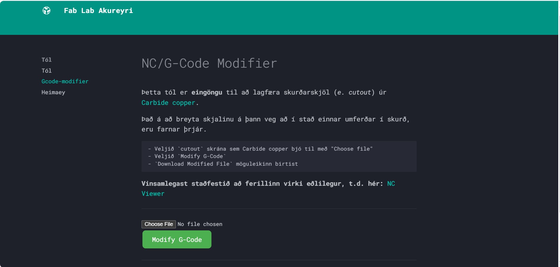
G-Code Midifier, a brilliant piece of Code by Árni.
At this point, I am ready to start milling, but that is a different assignment.
Anoter part of this assignment is to submit a pcb design to a board house. In the past I have used JLCPCB so I will also do so now.
Since I did not use any other layers in my original design, I will submit it as is.
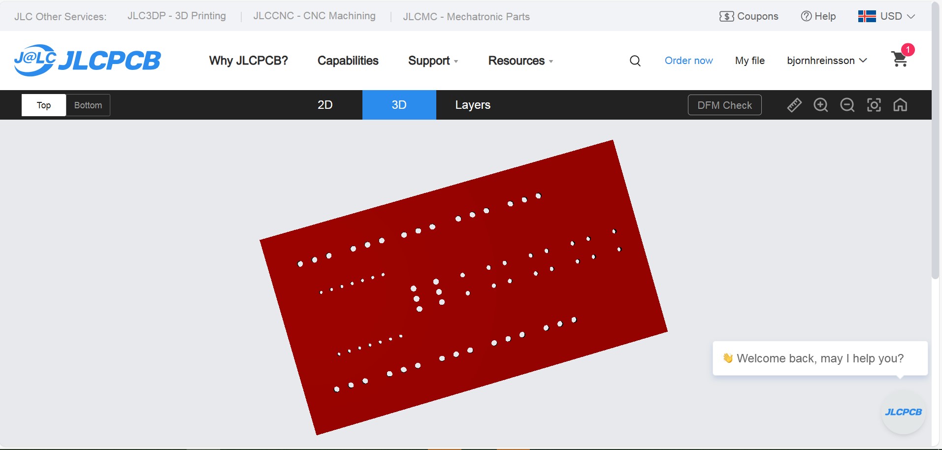
This is the top of the board, just holes, not silk screen or anything.
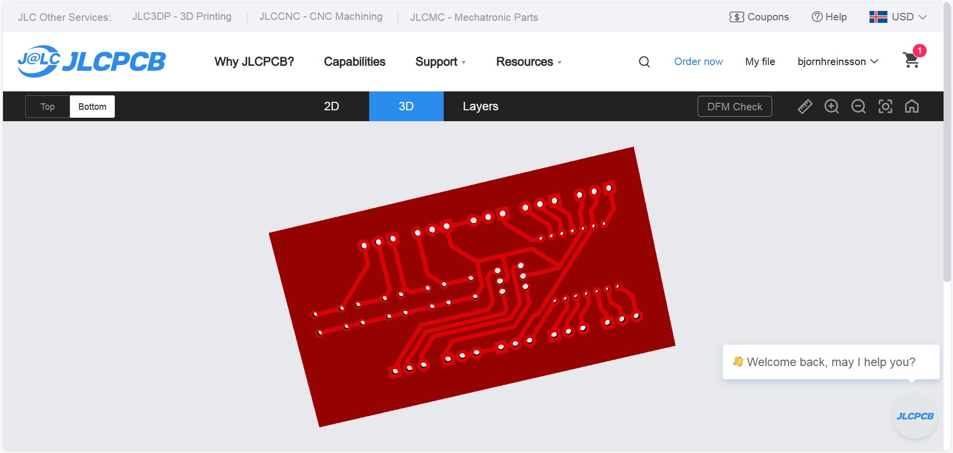
And this is the bottom side, no fancy pancy, just the tracks.
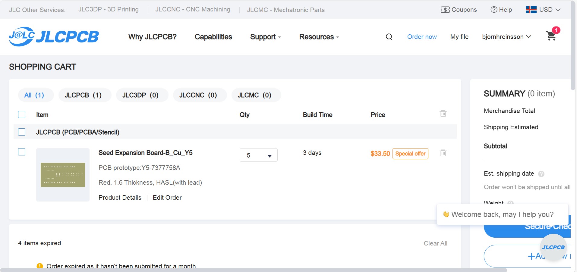
And for 5 pieces of singel layer board, they wanna charge me 33.5 dollars, maby later.
Individual Assignment
Since we just got a XTool F1 Ultra 20W Fiber & Diode Dual Laser Engraver I decided to try it out. It is a completly different method than using the cnc machine. I had to export or save the KiCad project ad a DXF document, open it in Inkscape becuse we did not know how to get the drillfile along with the B.Cu. Then I added the holes onto the solder pads and starter the laser process. I was nott quite happy with the resault and while I was waiting for the laser to finish, I took a better look at KiCad and found out how to get the drill file out in DXF format. So I decided not to try again, but use the cnc process I know and is proven to work. Also, we could not cut the holes in the lasser, I would have to drill it by hand afterwards.

This is the new laser in FabLab Akureyri.
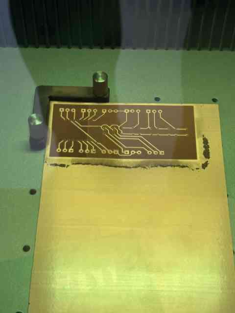
The job has started and is looking good.
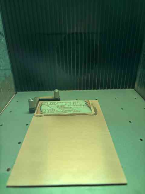
8 rounds later and job almost done.
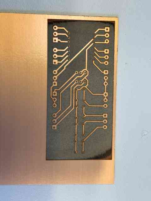
Here wer see the final resault, not quite happy with it.
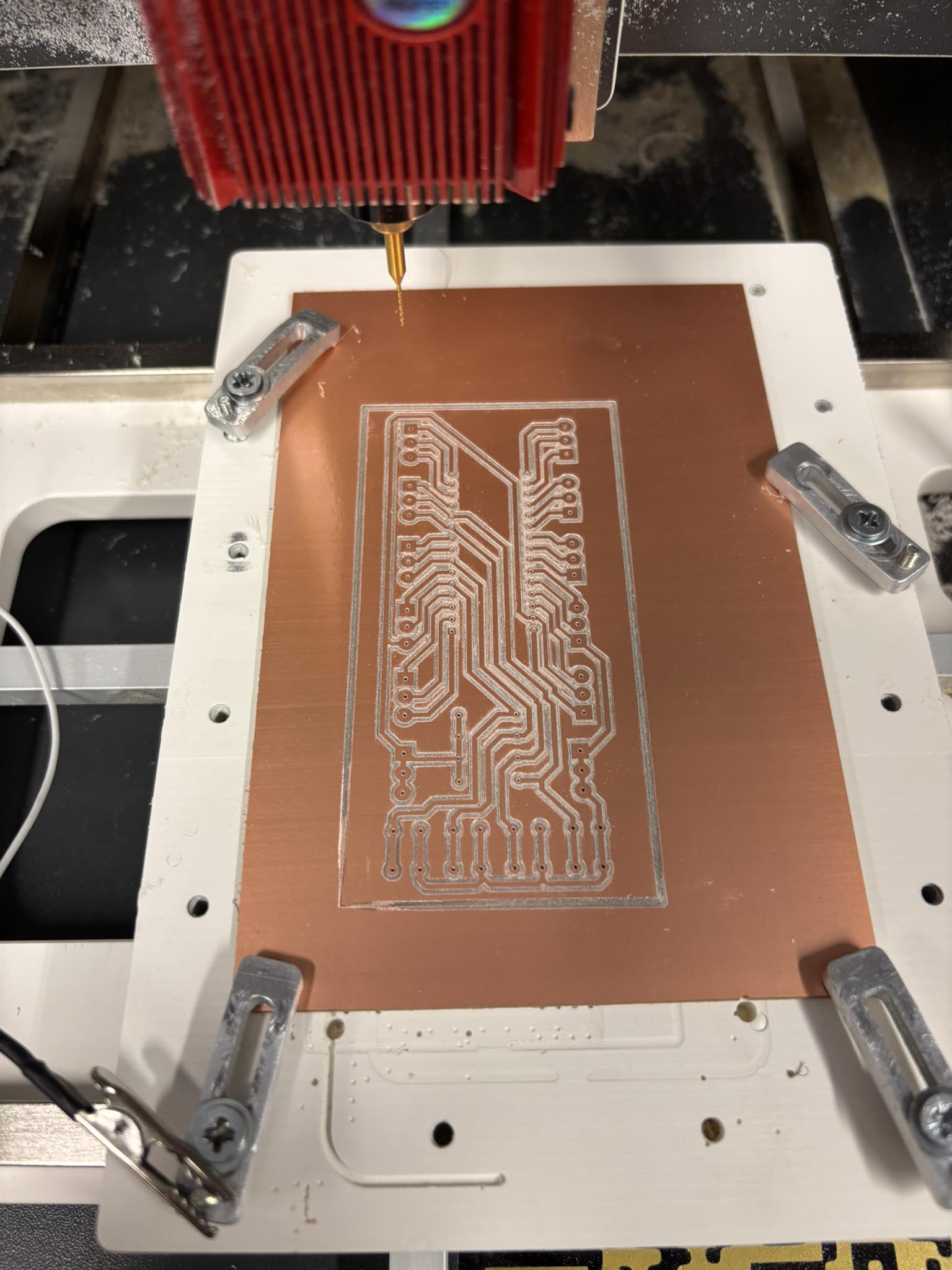
We have a couple of Wegstr cnc routers in the FabLab. Me and my students have been using them quite a bit so I am familiar with it. It´s a process I know and can easily do.
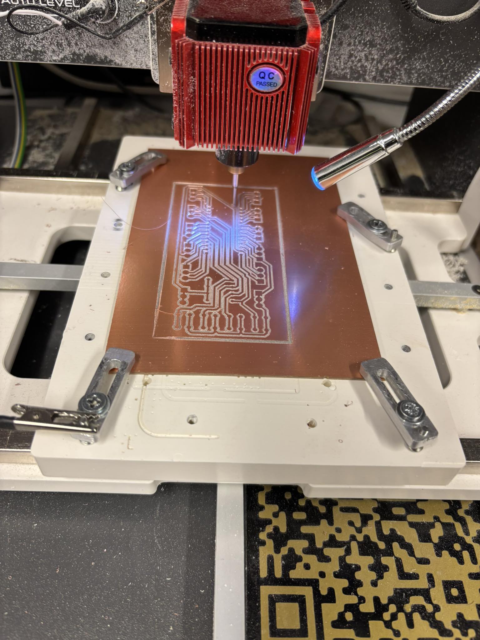
Wegstr cnc router cutting the b.Cu.
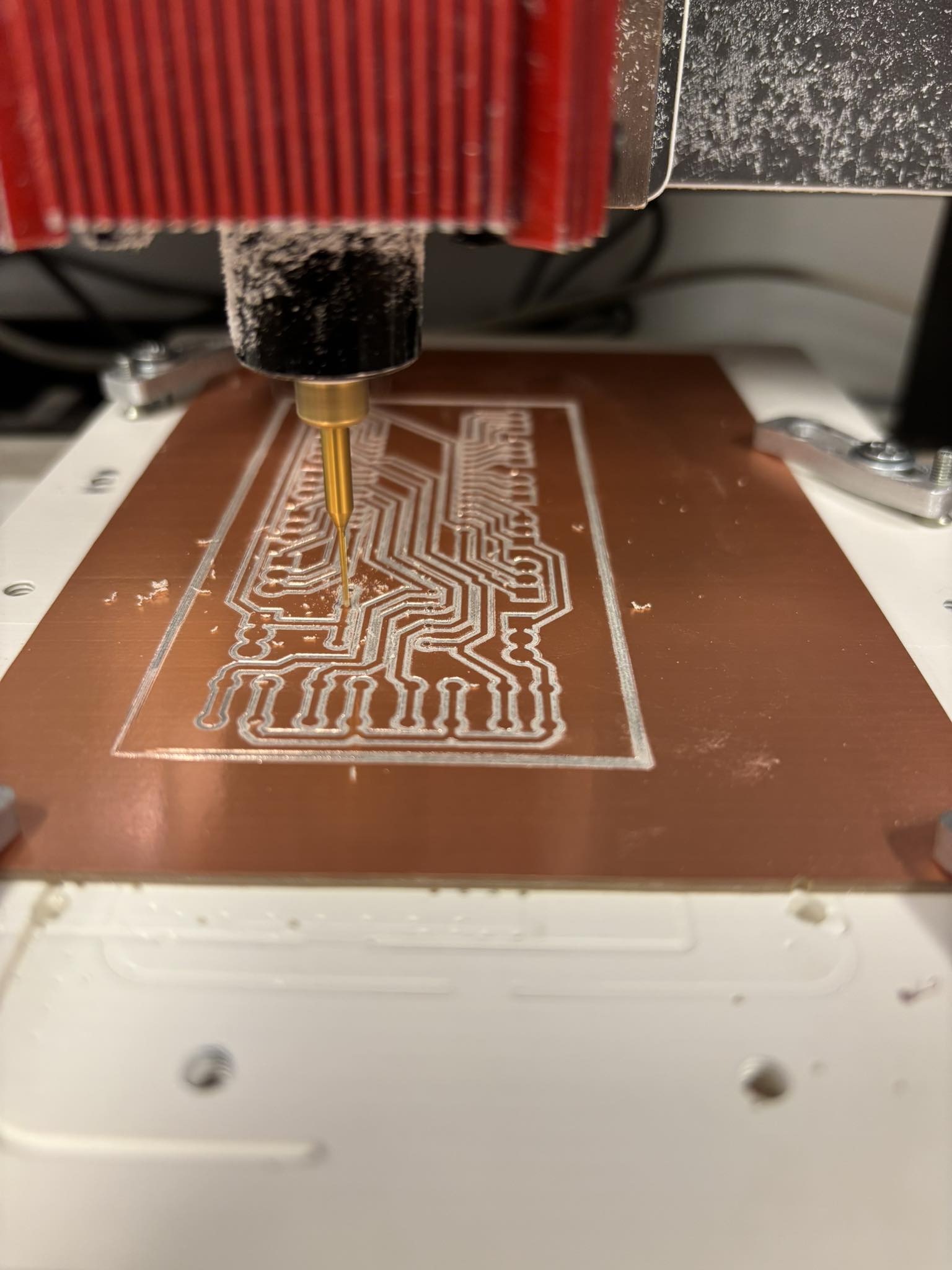
Trakcs finished and holes being drilled.
Started to fit the components.
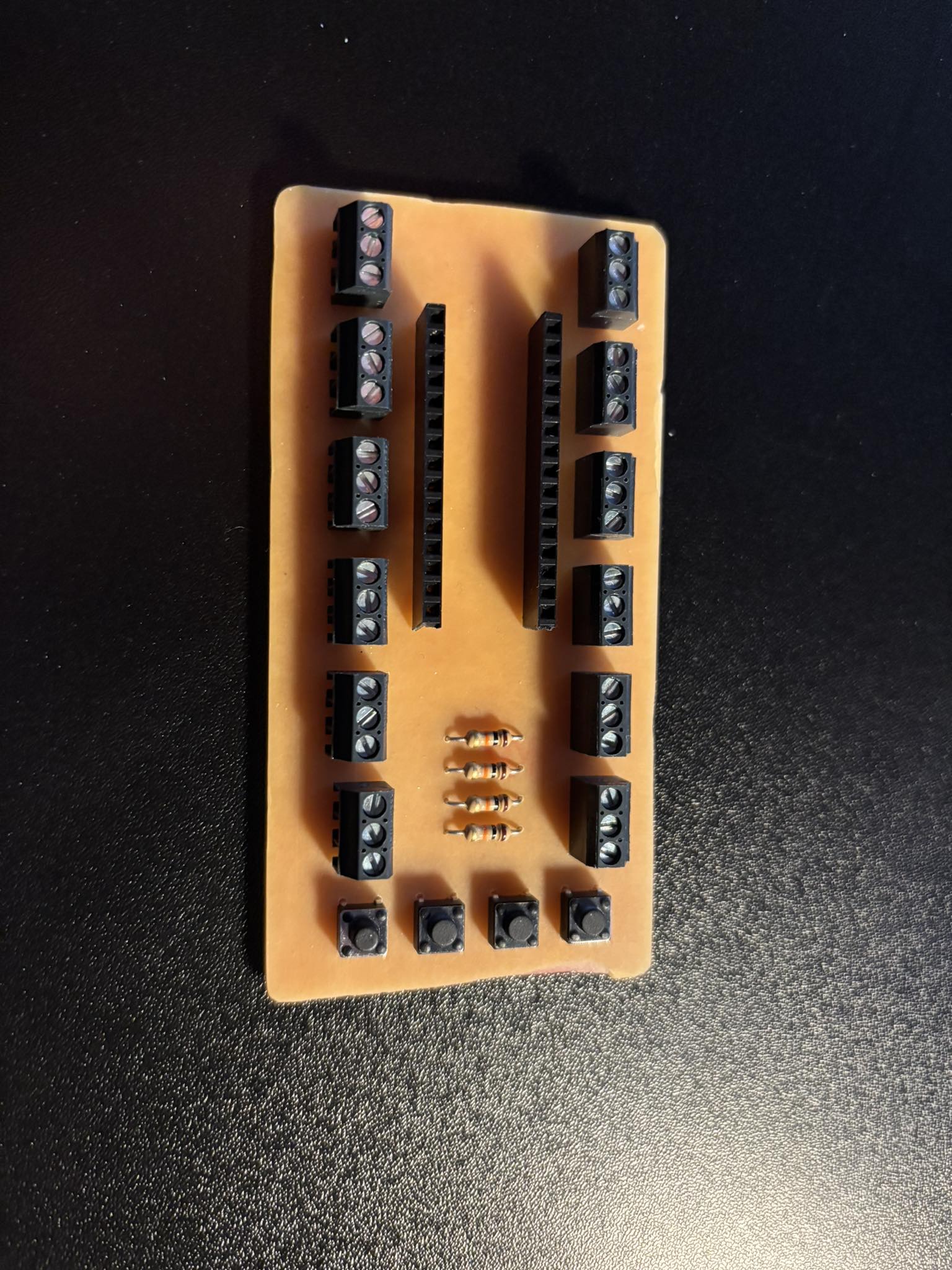
Here it is, all done, with the Seeed intalled and ready to be tested.
The seed is not soldered to the board so I can easily changed the microcontroller.