Week 04
Electronics Production
Brief Overview
Welcome to Week 4 of FabAcademy! This week's focus is on Electronics Production. In this assignment, we will delve into the process of designing and manufacturing electronic circuits. The key objectives include:
- Understanding the basics of electronics production techniques.
- Hands-on experience with designing and fabricating PCBs (Printed Circuit Boards).
- Learning soldering techniques for assembling electronic components.
- Applying quality control measures to ensure functional electronic prototypes.
My Heroshot for this Week
 |
 |
 |
 |
There are two types of assignments, one group and one individual.
Group Assignment :- Characterize the design rules for your PCB production process
During this week's group assignment, our focus was on Laser cutting and scanning. We formed three distinct teams to explore and conduct trials on the laser cutting machine. The primary objectives of the group assignment were as follows:
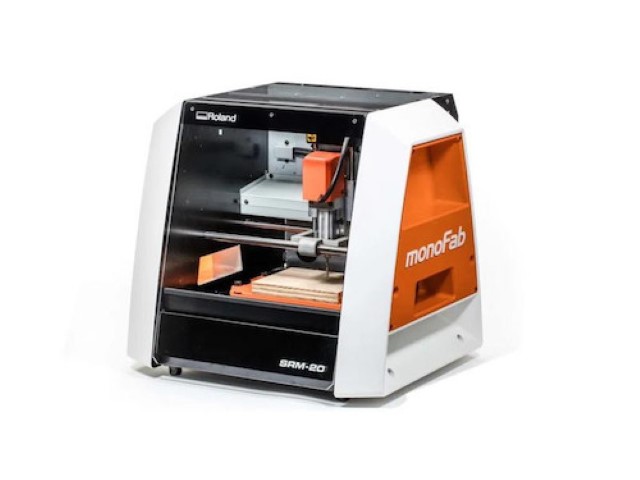
PCB Milling MAchine: Rolland SRM-20
- Comprehensive exploration of the PCB Milling machine and its specifications.
- Gaining insights into the technical details and capabilities of the machine.
Operational Knowledge:
- Acquiring practical knowledge on how to operate the machine effectively.
- Learning the step-by-step process of setting up and running the machine.
Safety Precationus:
- Understanding and implementing safety measures associated with operating the Machine.
- Emphasizing the importance of maintaining a secure working environment.
Optimization Parameters:
- Determining the optimum cut depth and min distance between two traces.
- Checking the diffrent end mills and observing its results: check the feeds, speeds, plunge rate, depth of cut (traces and outline) and tooling
PCB Milling Machine
A PCB milling machine is a computer-controlled device designed for precisely cutting printed circuit boards (PCBs).
Similar to a laser cutter, it employs a different method to achieve accurate results. Instead of a laser beam, the milling machine
uses rotating cutting tools to remove material from the PCB substrate, creating circuit traces and patterns. This process is highly
controlled and allows for the creation of intricate and customized circuitry. PCB milling machines are essential in the electronics
prototyping and production process, enabling the quick and precise fabrication of PCBs without the need for chemical etching. At our
Vigyan Ashram Fablab, we utilize the Rolland MonoFab SRM-20 PCB Milling Machine for experimentation and trials.
 |
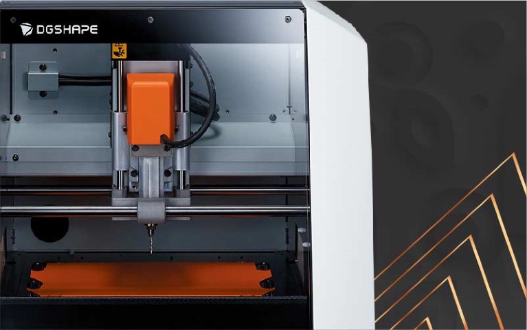 |
Rolland MonoFab SRM-20
The Rolland MonoFab SRM-20 is a versatile PCB milling machine equipped with advanced features for accurate and efficient PCB fabrication.
Using computer-controlled precision, this machine precisely mills away the unwanted copper, creating intricate circuit patterns. It offers
a user-friendly interface and is suitable for professionals and hobbyists alike. The SRM-20 streamlines the PCB production process, making it
an indispensable tool for rapid prototyping and small-scale PCB manufacturing. A wide range of materials, including modeling wax, chemical wood,
foam, acrylic, poly acetate, ABS and PC board can be precision milled using the SRM-20 small milling machine, allowing you to create realistic 3D
prototypes that are virtually identical to production parts. Its capabilities extend to various materials used in PCBs, ensuring a clean and precise result.
Visit our Group assignment page here
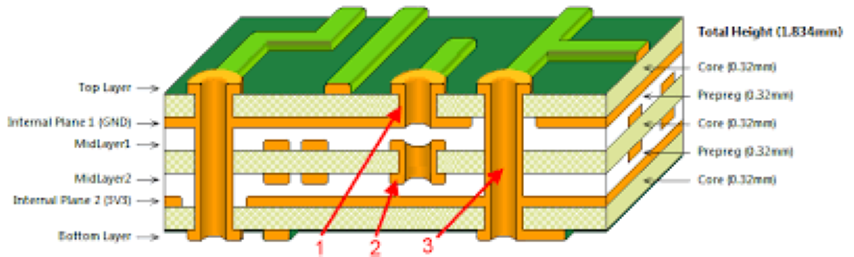
PCB (Printed Circuit Board) fabrication
Printed Circuit Board (PCB) fabrication is a critical step in the electronics production process, serving as the foundation for assembling and connecting electronic components. PCBs are flat, rigid boards made of insulating material, typically fiberglass-reinforced epoxy, with conductive pathways etched or printed onto the surface to create a circuit.
The fabrication process involves several key steps, including design, substrate preparation, layering, etching, and finishing.
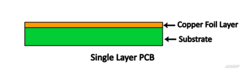
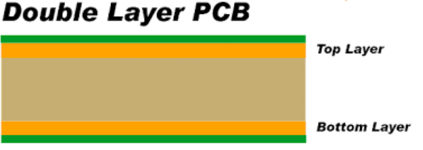
There are different types of PCBs, each catering to specific applications and requirements :
Single-layer PCBs:
|
 |
Double-layer PCBs:
|
 |
Multi-layer PCBs:
|
 |
PCB Fabrication (Process, Material, Machine and Tools)
Etching for PCB Fabrication
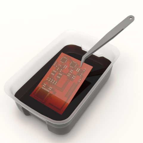
Process:
Traditional etching involves using strong acids or mordants to cut into unprotected metal surfaces. Modern variants include microfabrication etching and photochemical milling, crucial for circuit board production.
Chemicals Used:
- Acetic acid (CH3COOH)
- Citric acid (C6H8O7)
- Hydrochloric acid/Muriatic acid (HCl)
- Hydrogen Peroxide (H2O2)
- Sodium chloride (NaCl)
- Copper sulfate (CuSO4)
Precautions:
- Proper waste management to avoid environmental hazards.
- Avoid reusing etching solution for efficiency and cleanliness.
- Neutralize acid with sodium bicarbonate, precipitating copper for safe disposal.
Machining (Milling) for PCB Fabrication
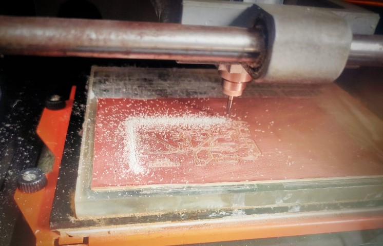
Process:
Printed circuit board milling removes copper from a PCB sheet to recreate pads, traces, and structures according to a digital layout file. A subtractive, non-chemical process suitable for office or lab environments. Quality depends on milling accuracy, bit condition, and control, contrasting with the chemical etch process.
Material:
- FR1-Phenolic paper, a tough wood fiber and phenolic polymer board (FR-1 and FR-2).
- Epoxy film electrical tape with a thermosetting acrylic adhesive.
- Electronic components.
Machine:
PCB milling machines are akin to miniature, accurate NC milling tables. Controlled via serial or parallel port connections to the onboard controller. Examples include the Roland SRM-20, featuring precision three-axis machining for PCBs.
Tools:
Conventional endmills, especially flat end mills, are suitable for machining PCBs. Flat end mills provide consistent trace width and efficient material removal.
Categorizing PCB Components
Printed Circuit Boards (PCBs) are essential components in electronic devices, and they host various types of components that play specific roles in the circuit. Here are some common types of PCB components:
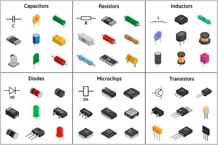
- 1.Resistors: Limit the flow of electric current.
- 2.Capacitors: Store and release electrical energy.
- 3.Inductors: Store energy in a magnetic field.
- 4.Diodes: Allow current to flow in one direction.
- 5.Transistors: Amplify or switch electronic signals.
- 6.Integrated Circuits (ICs): Complex assemblies of multiple components.
- 7.Connectors: Link different parts of the circuit.
- 8.Switches: Control the flow of current by opening or closing a circuit.
- 9.LEDs: Emit light when current passes through.
- 10.Transformers: Change the voltage level in a circuit.
- 11.Crystal Oscillators: Provide a stable frequency reference for timing.
- 12.Sensors: Detect changes in the environment and convert them into electrical signals.
- 13.Voltage Regulators: Maintain a constant voltage level in a circuit.
Through Hole v/s SMD Components
Printed Circuit Boards (PCBs) can accommodate electronic components in two main categories: Through-Hole Technology (THT) and Surface Mount Device (SMD) Technology. Each has its advantages and is suitable for different applications. Here's an overview of both:
Through-Hole Technology (THT):
Components: Through-hole components have wire leads that are inserted into holes in the PCB and then soldered on the opposite side.
Assembly Process: Manual assembly is common for through-hole components. The components are often larger and more spaced out, making it easier for manual soldering.
Strength and Durability: THT components tend to be more robust, making them suitable for applications where mechanical stress is a concern, such as connectors or components subjected to frequent plugging/unplugging.
Prototyping and Testing: Through-hole components are often preferred for prototyping due to their ease of use and reworkability.
Surface Mount Device (SMD) Technology:
Components: SMD components are smaller and have solder pads on the same side of the component, which is directly mounted onto the surface of the PCB.
Assembly Process: SMD components are typically assembled using automated pick-and-place machines. This allows for faster and more cost-effective mass production.
Space Efficiency: SMD components take up less space on the PCB, making them suitable for compact and miniaturized electronic devices.
High-Frequency Applications: SMD components are often preferred in high-frequency applications because the shorter lead lengths reduce parasitic capacitance and inductance.
Cost and Production: SMD components are generally more cost-effective in large-scale production due to automated assembly processes and reduced material usage.
In modern electronics, a combination of both through-hole and SMD components may be used on a single PCB. This is known as mixed-technology assembly. Through-hole components might be chosen for certain critical or high-stress parts, while SMD components are used for smaller, more densely populated areas of the board.
Individual Assignment
Tasks:-
-
Operate PCB Milling
Learn how to operate PCB milling milling for the fabrication process.
-
Make an In-Circuit Programmer with a Microcontroller
Create an in-circuit programmer that includes a microcontroller for programming tasks.
-
Mill and Stuff the PCB
Perform milling processes on the PCB and complete the assembly by placing components.
-
Try Other PCB Processes
Explore and experiment with various PCB fabrication processes beyond milling and stuffing.
-
Program and Test the PCB
Write code for the microcontroller, program the PCB, and conduct testing to verify its functionality.
To Operate PCB Milling Machine:
Download or Create your own Trace file
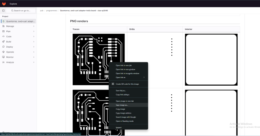
In this assignment we have a task to mill the quantorres trace file, so we visit the FabAcademy website and refered the PCB trace file.
A trace file window will be opened, so download and save it.
Now open MODs CE webpage on your web browser

Right Click and select "Program"
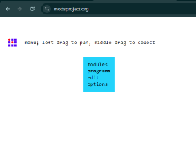
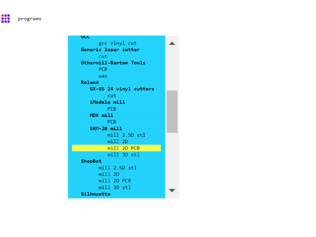
A new tab will be open, now select open program

Scroll down to select SRM-20 Mill 2D PCB
A new Window will be opened, having many block
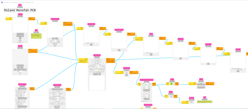
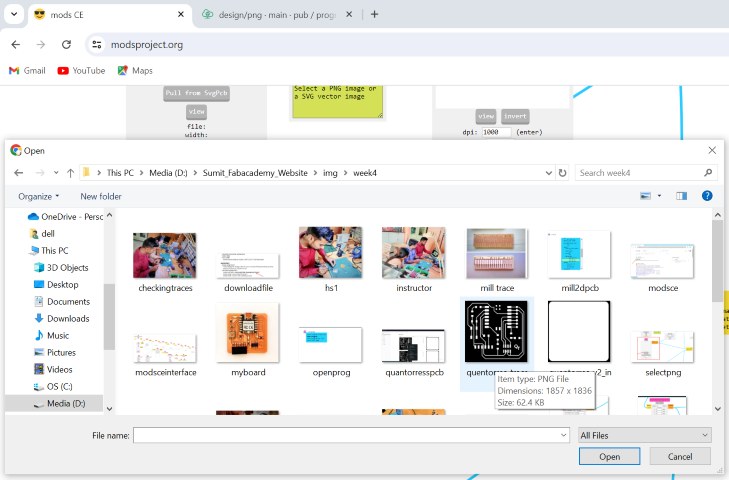
You can zoom, to the block of "select png"
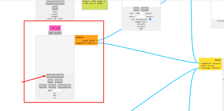
Select the trace, that you have downloaded or creating a SVG/PNG file using design software
Shift to another block to set Origin at 0,0,0
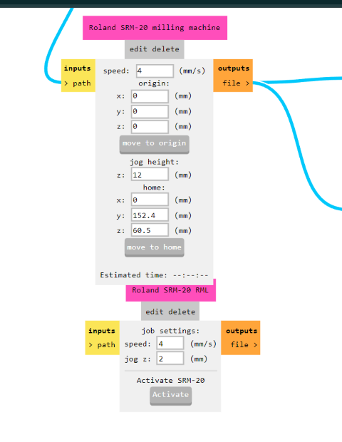
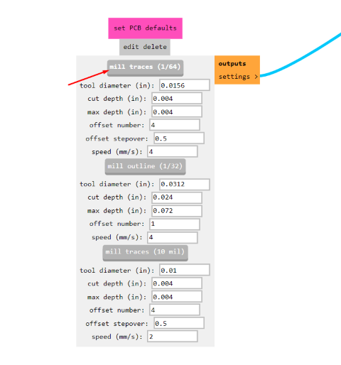
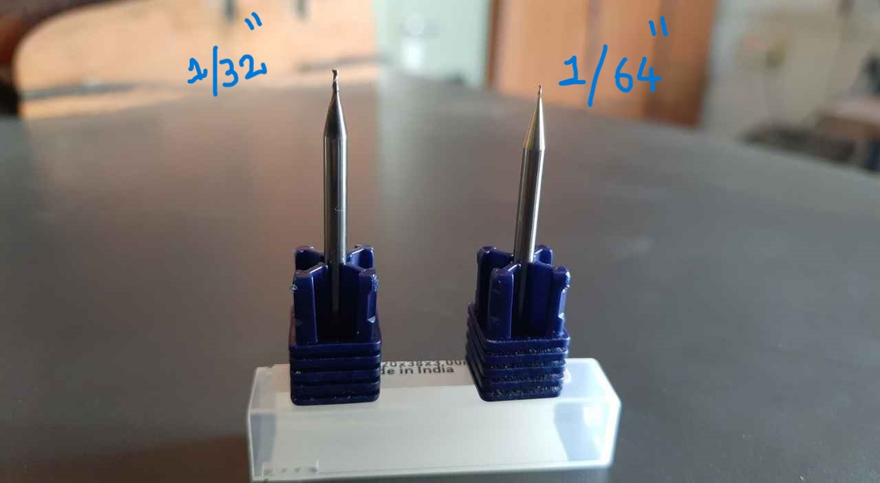
Pan left to select the tool,for milling 1/64 i.e 0.4 mm, for edge cutting 1/32, 0.8mm
Pan Right to Mill 2D Raster
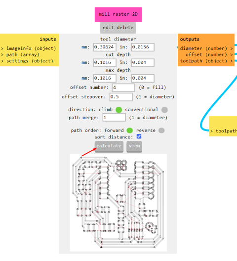
Do the Output Setting to save as a File
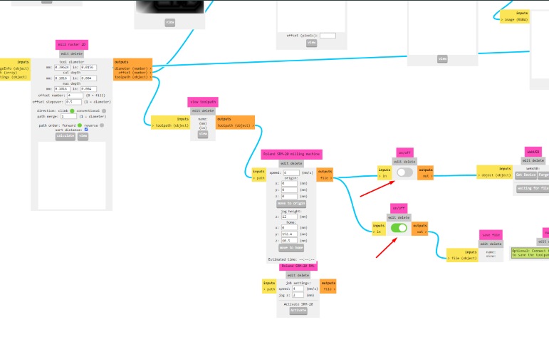
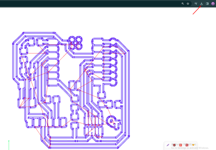
You can view the .rml file to check the toolpath
Milling Setup:-
Milling Tool and Material
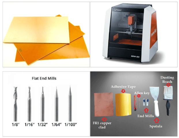
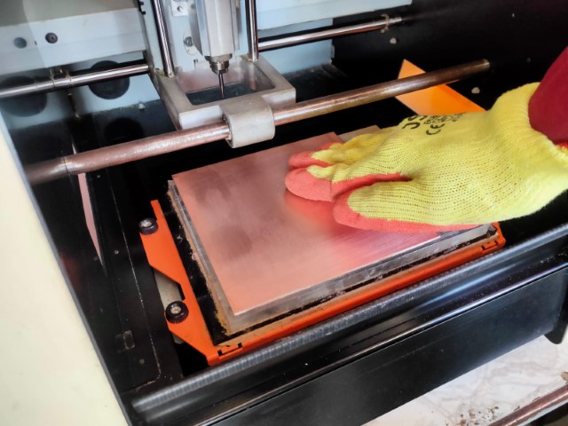
Mounting Cooper Clad PCB Board on Machine
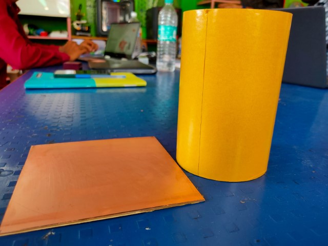
Apply Tape on the non copper side of the board
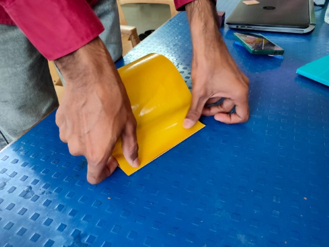
Clean the machine bed before mounting a new board for smooth even surface
Now remove the flim of the tape and mount the board on the machine bed, and press evenly to untrap the air bubbles.
'
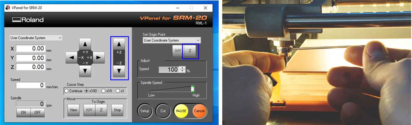
V-Panel Setting, to set the origin and send output.
PCB milling is high accuracy process, so need to sets all the parameters with atmost care and to correct values.
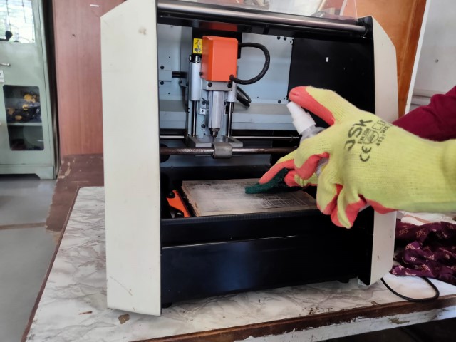
Open V-Panel Software on you System connected with the SRM-20 Milling Machine
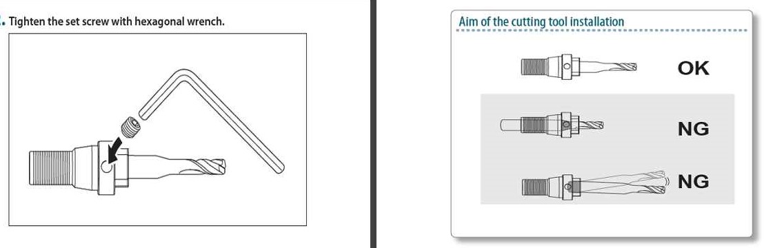
Mount the End Mill on the Colate
So we use 1/64 end mill for Milling the traces and 1/32 for cutting the traces
Now move the X,Y,Z axis on the V-panel to navigate the End Mill on the Origin Point
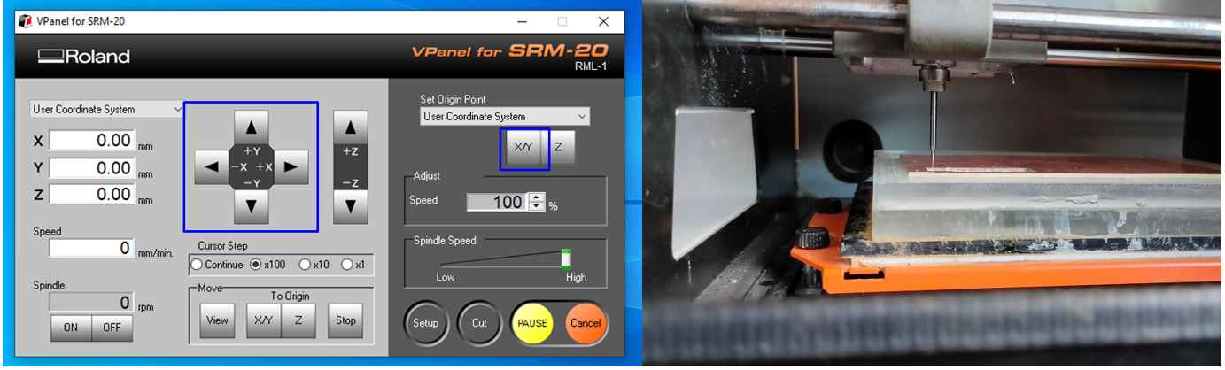
To Set Z bring the Z-axis slowly down and stop at some point 5mm above the surface. (There is the risk of damage to end mill due to pressure on the surace)
To avoid this we stop the Z-axis 5mm above milling surface and then release the alley screw so that the end mill fall down on the surface and then again we tighten the screw.
Now its time to Send the .rml Milling toolpath file to output, click on Cut and add a new the file from device and give output, remember to delete the previous files.
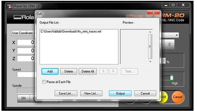
Similarly Follow the steps for Outer edge cutting file, but do it with 1/32 End mill and do not replace the X,Y Coordinates.
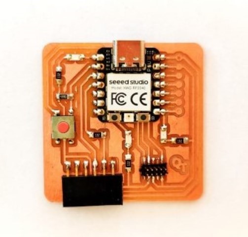
Taking out the milled board properly with anydame to Board, Machine and Traces.
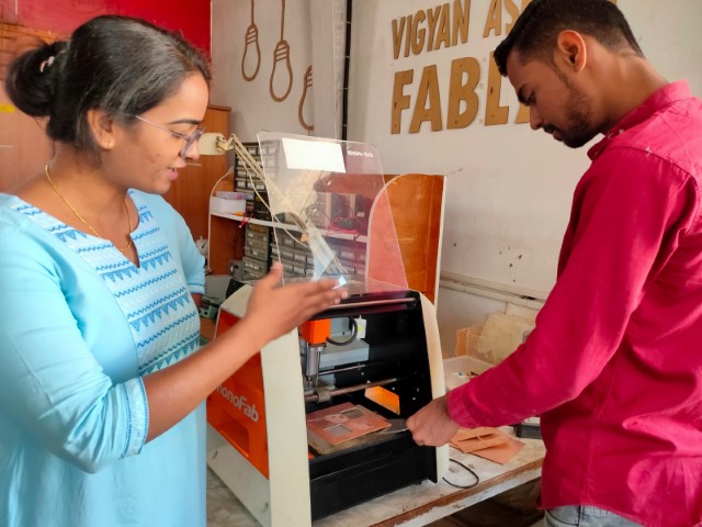
Milled Output ready for Stuffing and Soldering
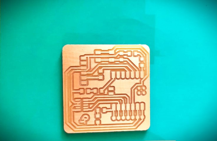
Checking the mill traces with Multimeter
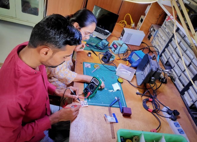
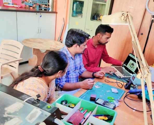
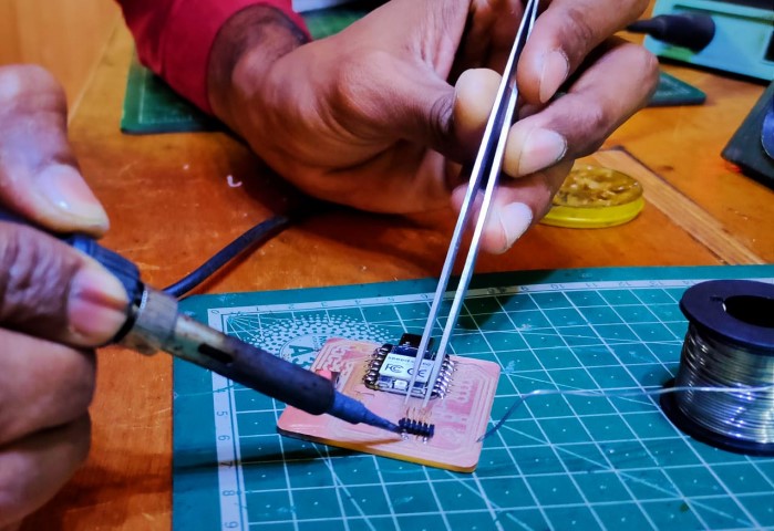
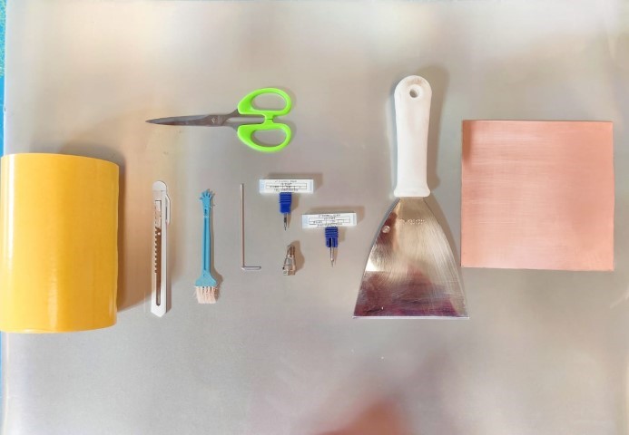
Soldering the PCB you will need this Tools and Equipment

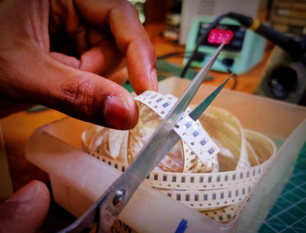
Collecting all ICS, SMDs and connector from your FAB inventory
Soldering all the Component properly at the correct position and orientation
Finally Now the Board is ready for Testing and Uploading the code.
Uploadind a code and testing the board
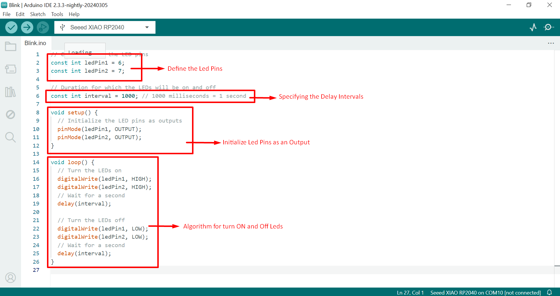
How to Upload the Code to Your Arduino
- Open the Arduino IDE.
- Copy the code below and paste it into a new sketch:
        // Constants for the LED pins

        const int ledPin1 = 6;

        const int ledPin2 = 7;


        // Duration for which the LEDs will be on and off

        const int interval = 1000; // 1000 milliseconds = 1 second


        void setup() {

          // Initialize the LED pins as outputs

          pinMode(ledPin1, OUTPUT);

          pinMode(ledPin2, OUTPUT);

        }


        void loop() {

          // Turn the LEDs on

          digitalWrite(ledPin1, HIGH);

          digitalWrite(ledPin2, HIGH);

          // Wait for a second

          delay(interval);


          // Turn the LEDs off

          digitalWrite(ledPin1, LOW);

          digitalWrite(ledPin2, LOW);

          // Wait for a second

          delay(interval);

        }
- Connect your board to your computer.
- Select the correct board and port from the Tools menu.
- Click the Upload button (right arrow) to upload the code to your board.