
Electronic design week
assignment assignment assignment
group assignment:
- use the test equipment in your lab to observe the operation
- of a microcontroller circuit board
- send a PCB out to a board house
individual assignment:
- use an EDA tool to design a development board to interact
- and communicate with an embedded microcontroller
- extra credit: try another design workflow
- extra credit: design a case for it
- extra credit: simulate its operation
So first thing i did to prep for this week was to download KiCad and gather information and tutorials. Below is a playlist I made filled with KiCad tutorials I found on YouTube.
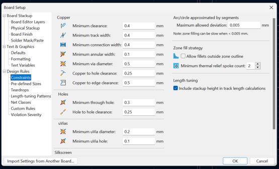
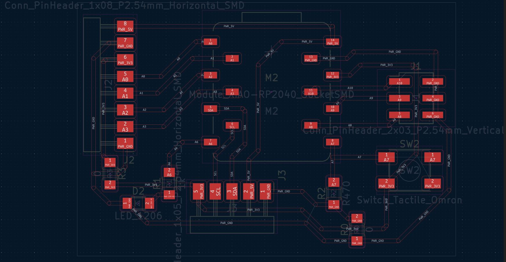
I began working with KiCad, I started by attempting to redo the Adrianino. This was by copying every single component in order to understand the workflow. First step was to set the rules. I put the width as 0.6 mm
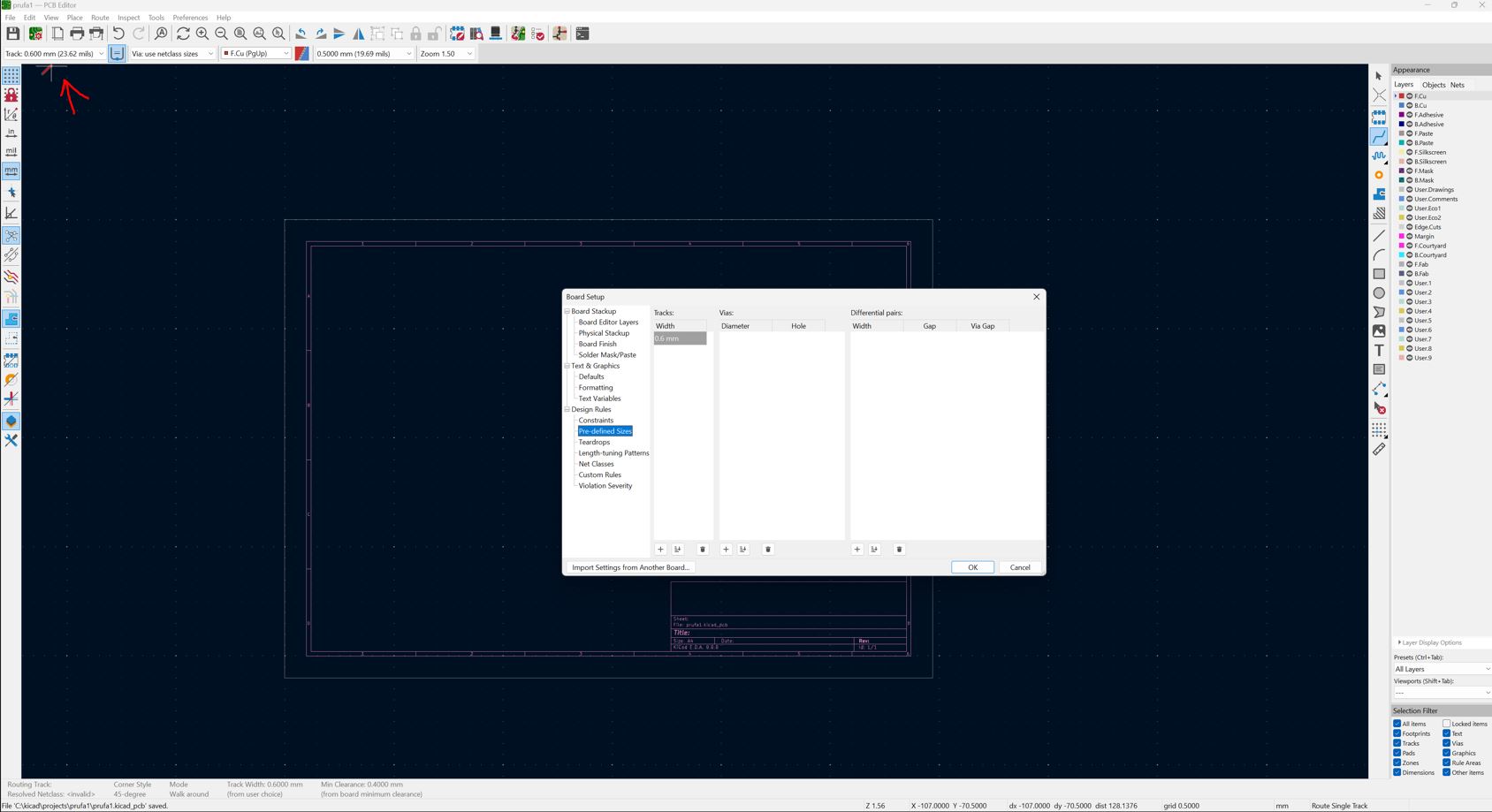
Another important thing was to set up the Fab Electronics Library for KiCad (instructions in link)
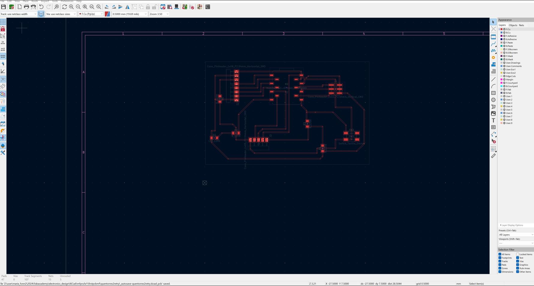
I had the Fab-Xiao sketcup on the side to attempt to replicate it. Mostly to figure out a better understanding of the parts and what they do. How the sketchup part affects the other sections etc. In the beginning I couldn't figure out why I could not connect the wires to the parts I wanted. Apparently I had to define it in the Schematic before continuing. I named the different paths and that way when I moved to the next step KiCad showed me how the wire placement should go with blue lines. After figuring that out I managed to redraw the board (although
 different since
I used sockets instead of pins).
different since
I used sockets instead of pins).w
Version 1 (BIGGer version)
It didnt look the exact same as Adrian´s since we used sockets instead of pins for the Xiao.
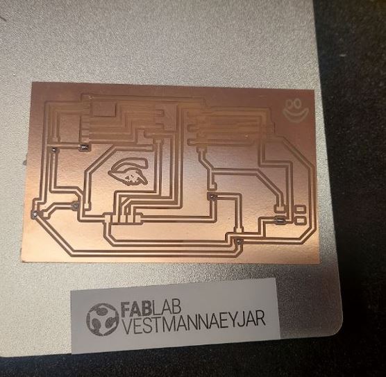
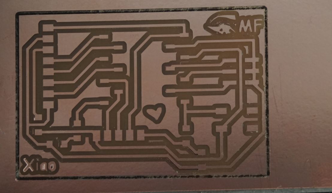
Here are the milling results:
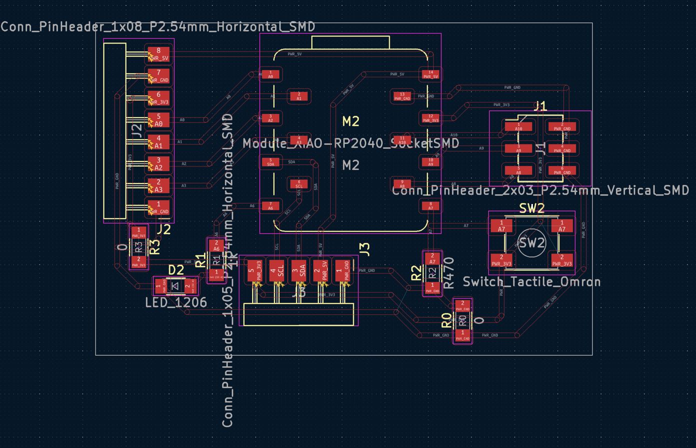
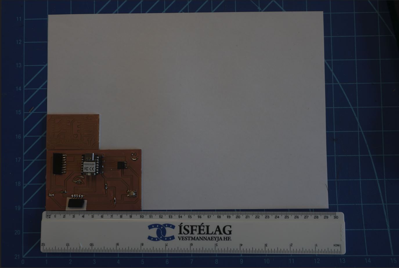
Version 2 (pocket sized)
I continued to make the circuit board smaller since having
it so big felt like a waste of precious space since there is
limited space for the placement within the shoe. I
changed the wiring and the placements to be closer together
so the board wouldn't be as gigantic. To my surprise I
managed to make it at least half the size of the original
one.
The design rules showed 4 errors, but those are due to the fact its a 0 OM resistor
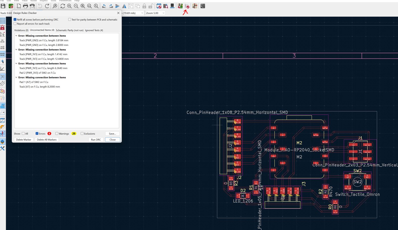
It was fine regardless of the error :)
I exported it to an SVG and made it so the background was dark and the part it needed to mill was white!
I then went through with the same progress on modsproject as i did in the Electronics production week
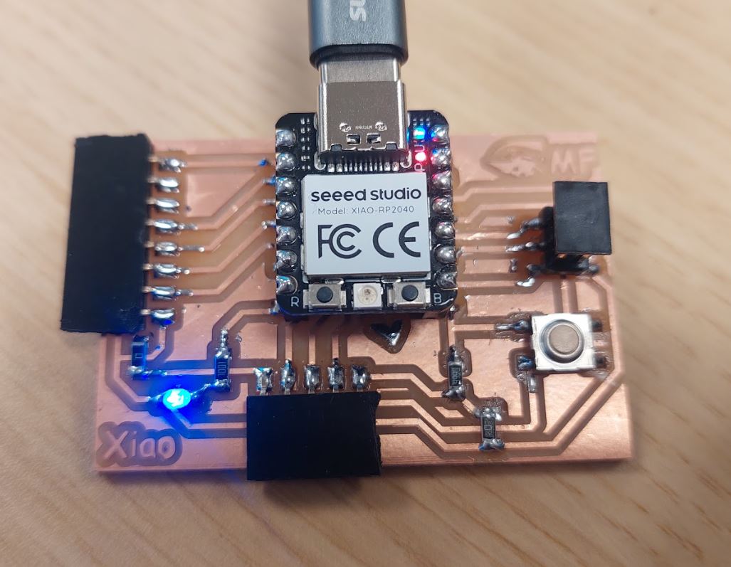
Here you can see it soldered >
(smaller version/version2)
Here is a side by side size comparison. (the version I will be using most in the project is the small one above, the original version is below)
Here it is soldered (version 2):
Bill of materials