WEEK 8 - Electronics Design
Checklist:
- Use an EDA tool to design a development board to interact and communicate with an embedded microcontroller.
Learnings from the group assignment
The group work involved using a multimeter and an oscilloscope to understand which signals to measure to verify the operation of a PCB board.
Design process and Result
Choosing the Microcontroller
First, it was necessary to decide which software to use to start designing the microcontroller PCB. Then, I decided which microcontroller to use for the design. In this case, I want to use an ATmega328P or an ATTiny44. To do this, I prepared a comparative of the most relevant characteristics:
Preparing EDA Software
After the group meeting, it was agreed to use Eagle software because it is embedded in Fusion 360 and also because it is the most versatile, theoretically allowing the generation of G code for PCB machining.
First, it was necessary to download Fusion 360 software using my educational account to gain access. I visited the (Autodesk student website), registered my account with the university domain (@ulima.edu.pe), and downloaded the program.
To start with the first step, which is the schematic design, it is necessary to download the component libraries used in Fab Academy. For this, I visited the main website of the week and accessed the (GitLab link) and downloaded the Eagle library.
I downloaded the code as a .zip file and saved it in my resources folder. To keep everything organized, I created a FAB LAB UL workgroup in which I created a project called Fab Academy 2024.

Importing Fab Academy Library
To enter the Eagle module, you need to create a library file. To do this, click on the file icon and select the "New Electronics Library" option:
Then, click on the "Import Libraries" icon and select the "Import from local disk" option:
Once in that menu, you should copy the "fab.lbr" file that we downloaded from GitLab into the folder path "libraries".
Verify that it has been added by entering the "Source" filter and selecting the "Local disk" checkbox:
Electronic design
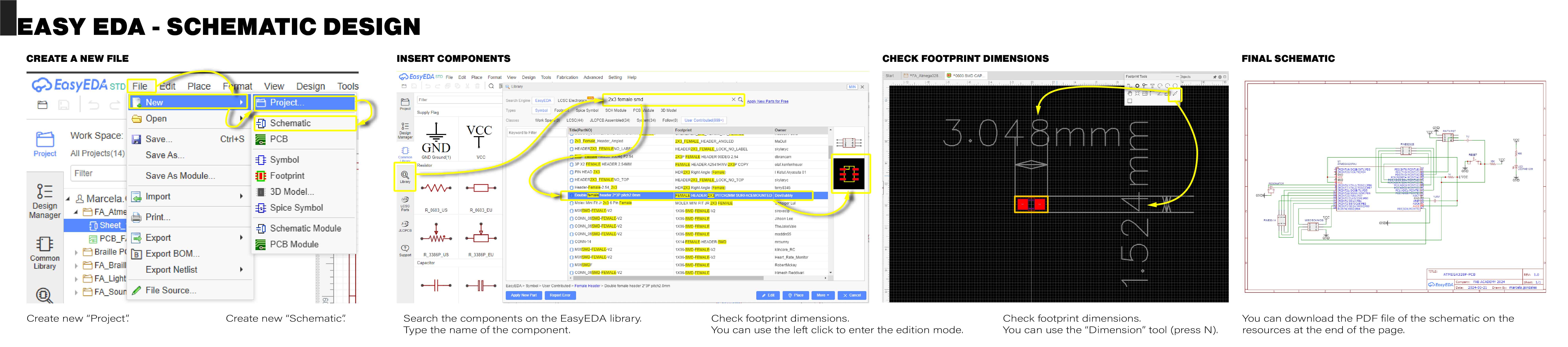
Schematic Design
To enter the Eagle module, you need to create a circuit file. To do this, click on the file icon and select the "New Electronics Design" option:
Then, create a schematic to design the connections of the PCB board by selecting the "New Schematic" icon.
In the search tab, choose each component one by one and place them in the design area.
To place the component in the design area, you can double-click or click and drag the component. To rotate it, right-click.
Connecting Components
After placing all the components, you need to connect them using nets:
- Add nets (a little bit messy):
Click on the "Net" tool from the toolbar. This tool allows you to draw connections between components. Click on a pin of one component and drag the line to the pin of another component to establish a connection.
- Label nets (more organized):
To keep the schematic organized and readable, label each net. Use the "Label" tool to assign names to the nets. This is especially useful for identifying connections that span different parts of the schematic.
- Add power and ground:
Ensure that all components requiring power are connected to the appropriate power source. Use the power (5V) and ground symbols from the library and connect them using the net tool.
- Check connections:
After all connections are made, use the "Electrical Rule Check" (ERC) tool to verify that there are no errors in the schematic. This tool will highlight any missing connections or potential issues. You can dismiss the warnings in the pins that have no connection.
- Review the schematic:
Review the entire schematic to ensure all components are correctly placed and connected.
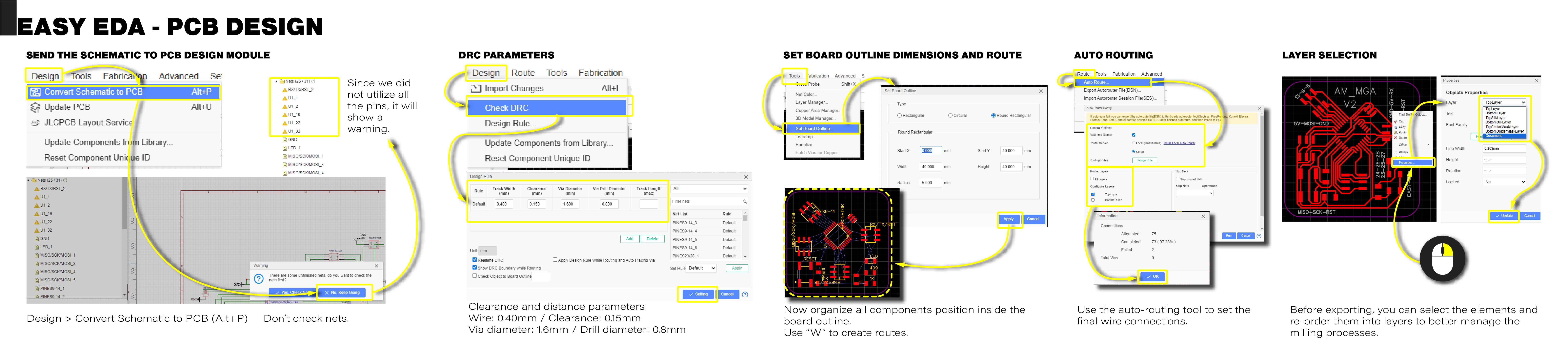
PCB Design
- Adding tracks or paths:
Tracks are the actual copper paths on the PCB that connect different components. Select the "Route" tool to draw these paths on the PCB layout. Carefully route the connections to avoid crossing tracks and to ensure a clean layout.
- Labeling connections:
Label each net to identify it easily. This is useful when the same net appears in multiple places in the schematic. To facilitate the identification of the pins when fabricating the board, I placed the numbers or names of the pins associated with the 6x2 headers.
- Check the design:
Once all connections are made and labeled, double-check the design for any missed connections or potential issues. Use the design rule check (DRC) tool to ensure there are no errors before finalizing the design.
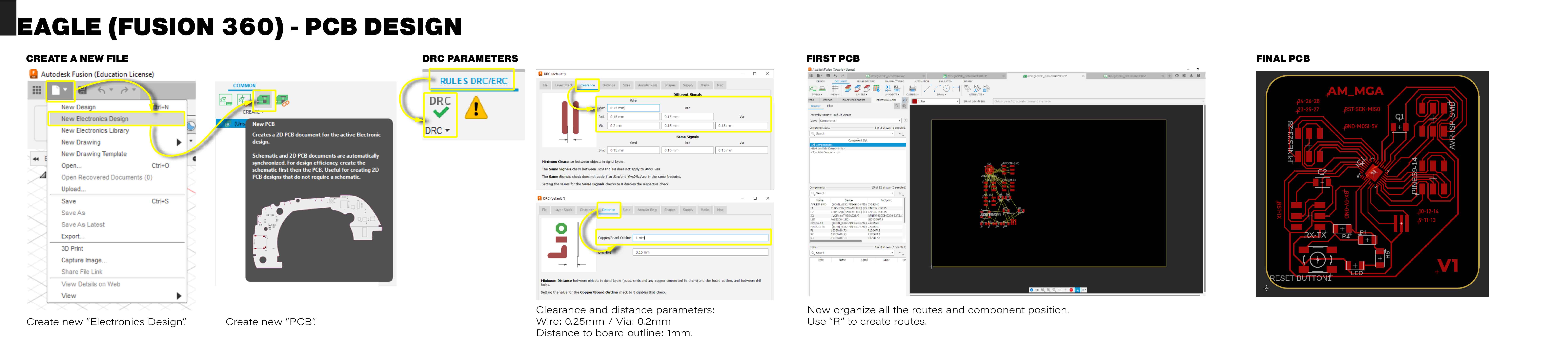
I manually routed the traces to have better control over their organization, ensuring that the layout would simplify both machining and component soldering.
I distributed the components considering how the pins would be used to connect the board, ensuring there was enough space for the connector headers.
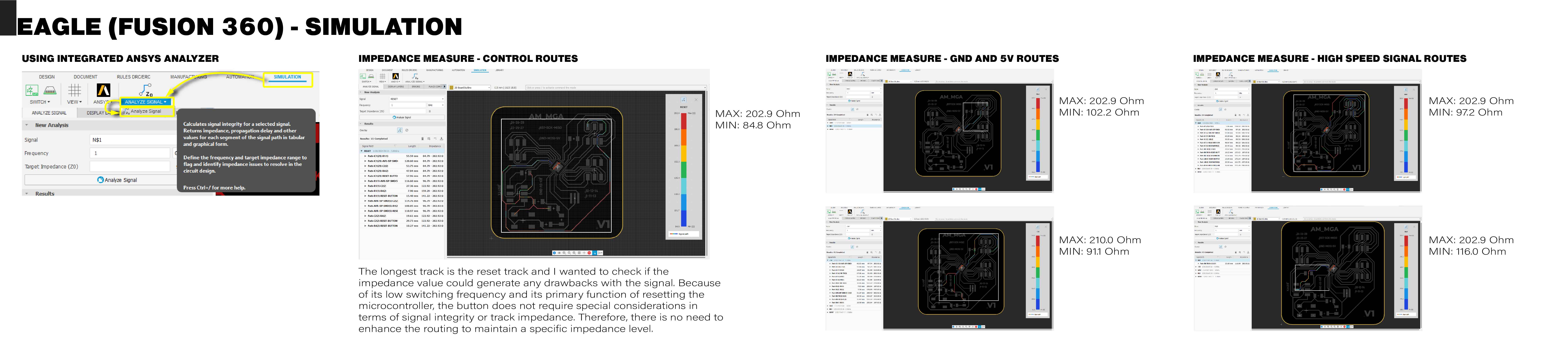
PCB Simulation
If the maximum impedance value obtained from my simulation for the longest track is 202.9 ohms, it means that the track impedance is relatively high. For low-speed signals, this may not be a significant problem, as signal integrity may not be significantly affected by impedance variations.
However, if I am designing for high-speed signals or have specific concerns about signal integrity, I may consider adjusting the track design to reduce impedance. This could be achieved by modifying the track width, spacing between tracks.
It is important to remember that the maximum acceptable impedance value may vary depending on my specific application and system requirements. If I am satisfied with the signal performance in my current design and am not experiencing signal integrity issues, I may not need to make additional adjustments to the track impedance. I will verify this when I fabricate and test it.
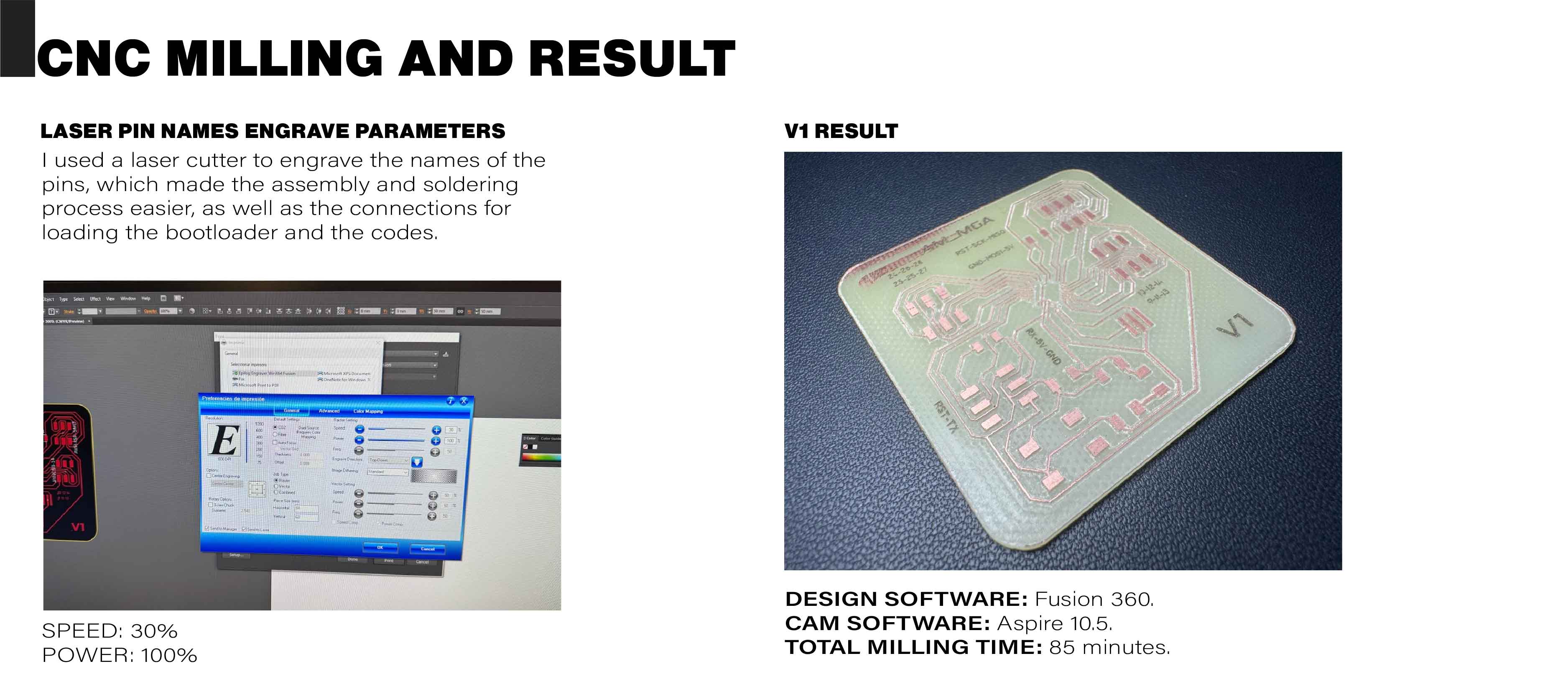
Export for Manufacturing
The board can be machined from the "Manufacturing" tab of the same software, but to expedite the testing process, I will use DXF and enable machining using Aspire. To do this, I go to the option Manufacturing > CAM Preview:

Result
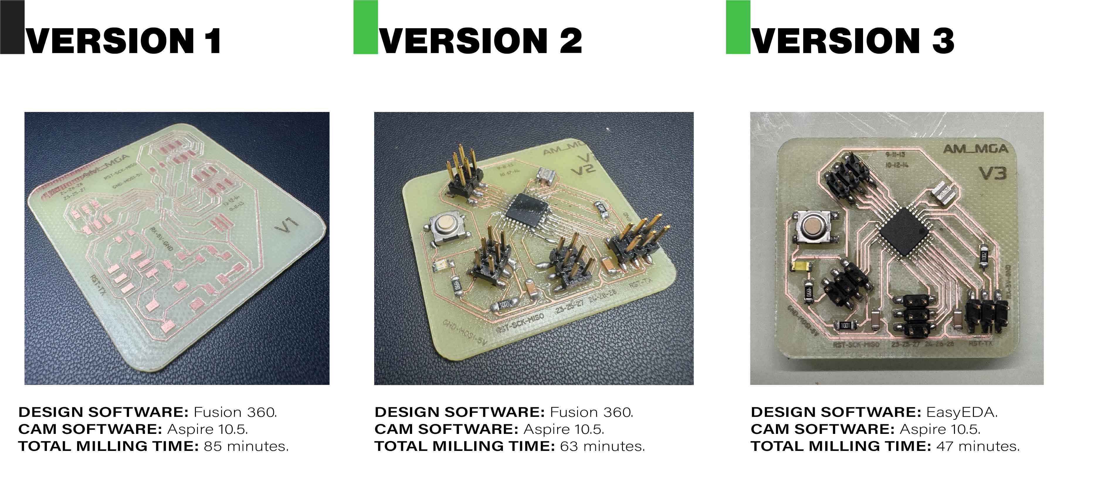
Schematic - V1

PCB - V1

V1 - PCB Result
Errors and fixings
Errors in V1
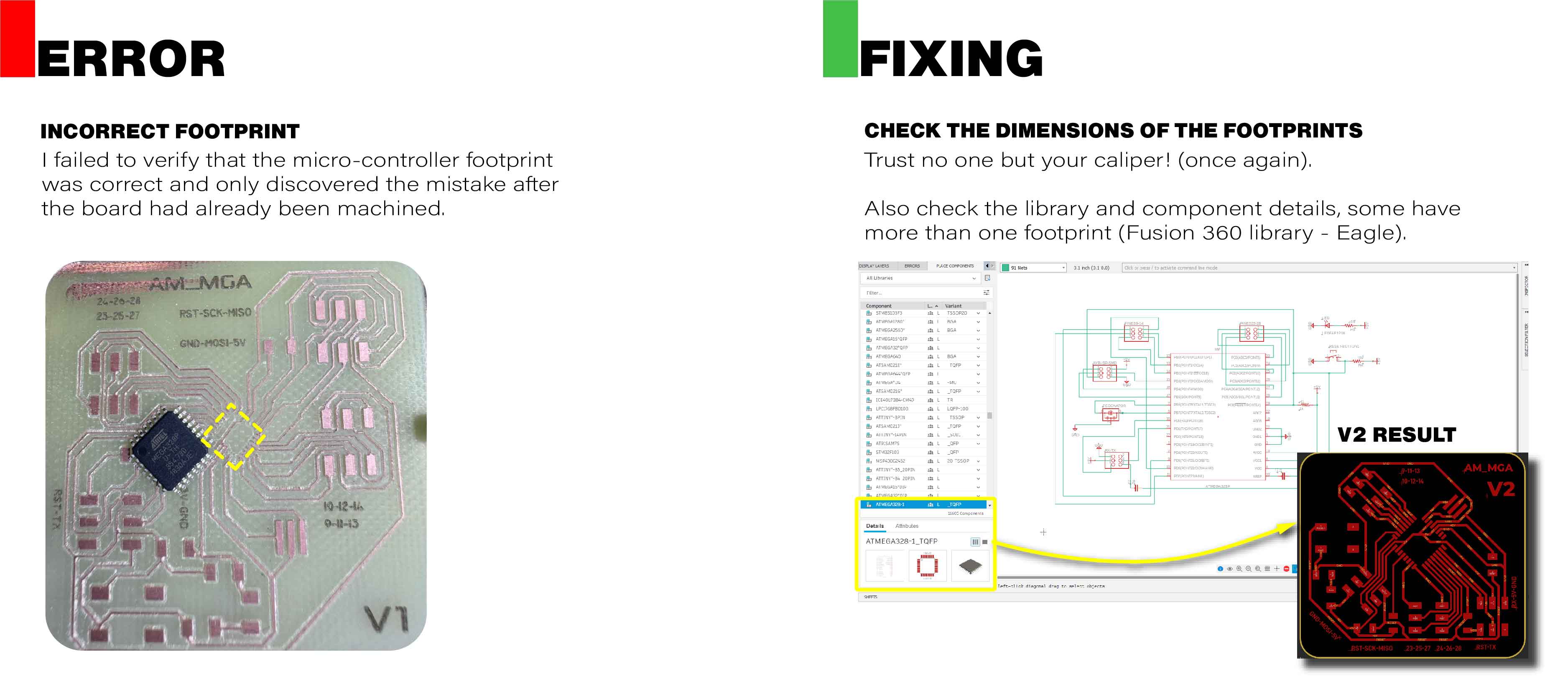
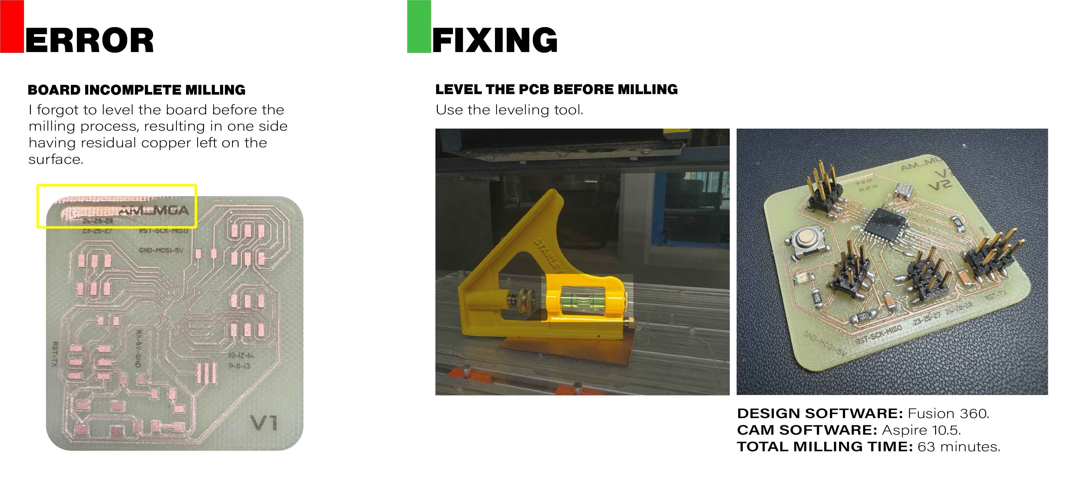
Learnings
Safety measures for using FR4 PCBs
When working with PCBs made from FR4 (Fiberglass) instead of the recommended FR1, it is crucial to follow stringent safety measures to protect your health and ensure a safe working environment. Here are the key safety protocols to follow:
Respiratory protection
Fiberglass can produce fine dust particles that are harmful if inhaled. To protect our respiratory system, we used the following precautions:
- Wearing N95 or higher-grade respirators to filter out airborne particles.
- Use a vacuum cleaner in the working area to reduce the concentration of dust.
- Regularly cleaning the workspace to remove any settled dust.
Additional safety measures
- Wearing protective clothing, including gloves and safety goggles, to prevent skin and eye contact with fiberglass dust.
- Maintaining a clean and organized workspace to minimize the risk of accidents.
- Proper disposal of fiberglass waste in designated containers to prevent contamination.
Redesign: EasyEDA
Schematic - V2
PCB - V2
PCB - Version comparison
Download resources
Editables
- Fusion 360 editable file
Editable files for PCB-V2
- EasyEDA DXF file
Editable files for PCB-V3
- EasyEDA PDF file
Editable files for PCB-V3
- EasyEDA PNG file
Editable files for PCB-V3
- Aspire editable files
Editable files for setting milling parameters in Aspire 10.5
Schematic
- EasyEDA schematic PCB-V3
Final schematic in PDF used in the version 3 of the PCB.