Assignments
- Characterize the design rules for your in-house PCB production process: document feeds, speeds, plunge rate, depth of cut (traces and outline) and tooling.
- Document the workflow for sending a PCB to a board house.
- Document your work to the group work page and reflect on your individual page what you learned.
Individual apport
- Ernesto: I had to make and test a microcontroller development board. Having done quite a few tests, it was possible to find the production parameters for mods.
- Jorge: For our group assignment on electronics production, I made significant contributions by experimenting extensively with the tool database in FlatCAM software to create a finely tuned tooling database.
- Marcela: I chose to work with Aspire because I had previous experience with the software, and also because it allows me to perform a pocket machining process, which greatly facilitates the soldering process of components on the PCB.
Process
Machine parts:
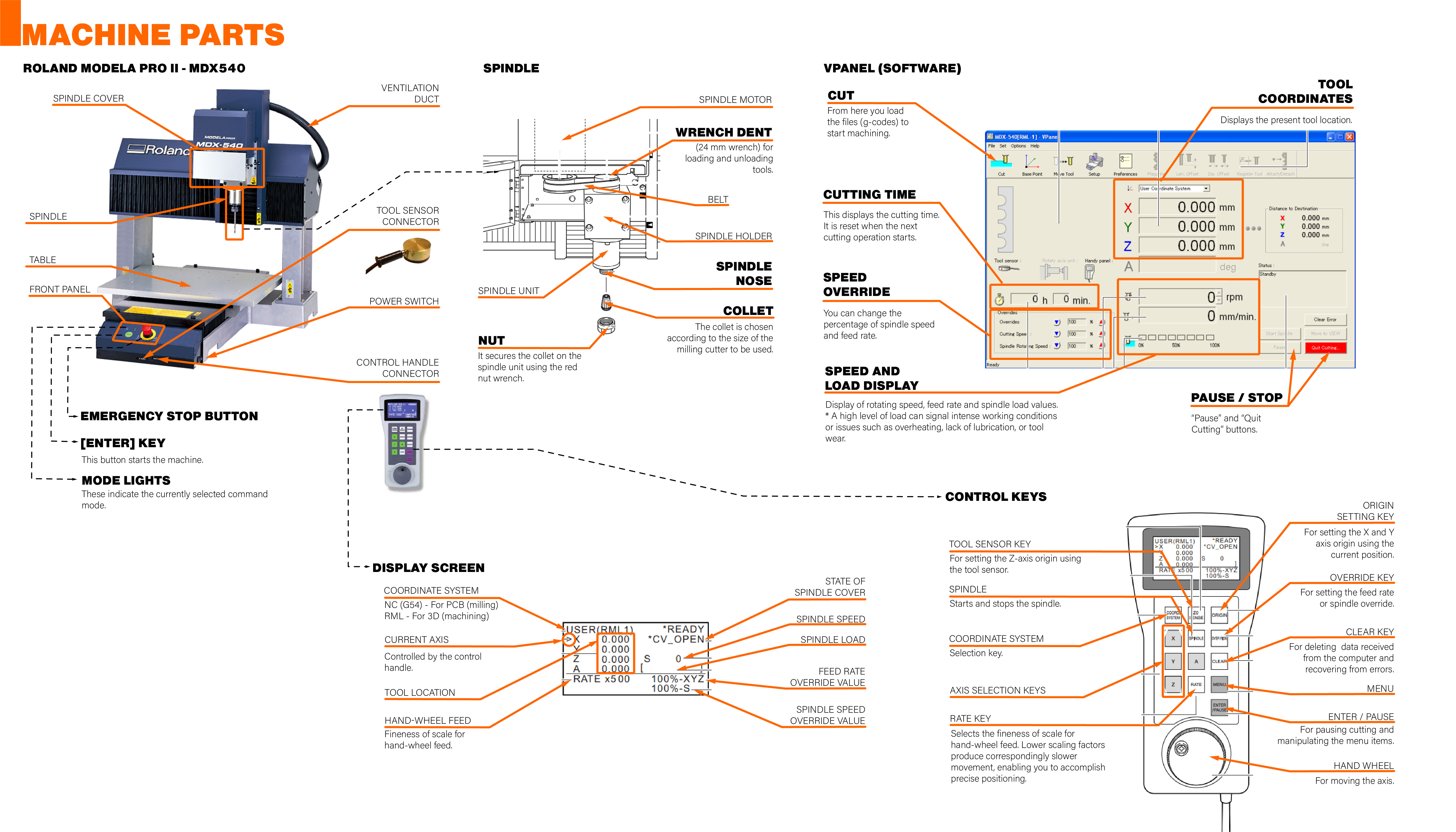
Machine Start-up Checklist:
- Turn on the power switch.
- Select the coordinate system (NC (G54) for PCB milling or RML for 3D machining).
- Press the "Enter" key.
- Ensure the required milling bit is installed.
File Checklist:
- Check the scale and cutting features of the file (G-code). You can use the NC viewer simulator.
- Review the initial part of the code: spindle speed (S12000).
- Review the final part of the code: to stop the job (M05 and M30).
- Load the file (G-code) into the "VPanel" software using the "Cut" tool.
Calibration Checklist:
- Check that the material is securely fastened to the platform.
- Ensure that the material measurement exceeds the size of the board you want to process by at least 3mm on each side.
- Verify that the platform is level on the X and Y axes using the leveling tool.
- Move the X and Y axes to the origin position used in your cutting file, ensuring they match (top or bottom, left or right).
- Place the end mill in the center of the board, attach the tool sensor, and calibrate the Z axis. For precise calibration, ensure you use a part of the tool sensor surface that is free from irregularities.
- You may proceed to start the cutting process.
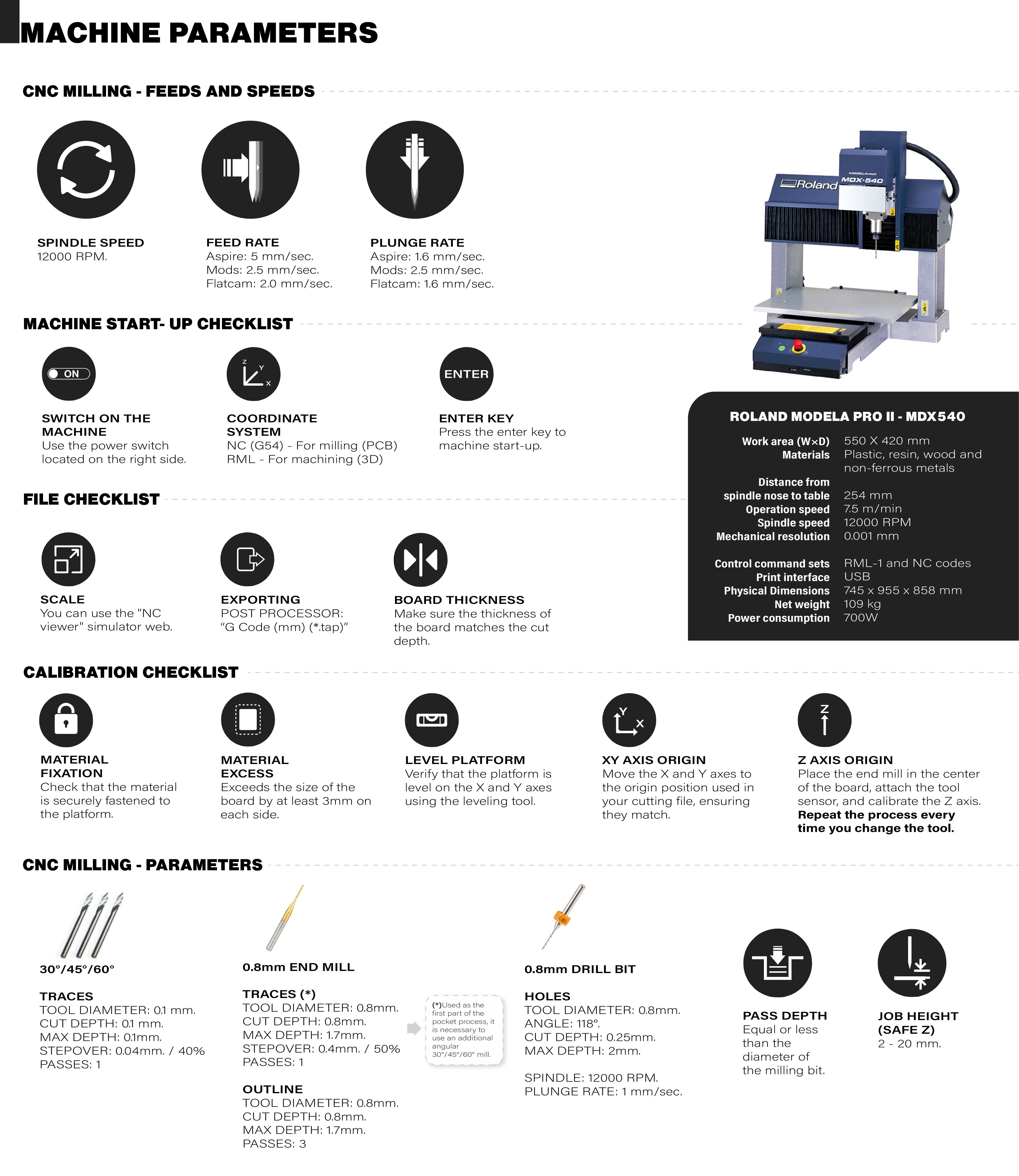
Machine Parameters:
Fab Lab UL PCB Production:
At the Fab Lab of the University of Lima, different software is used for PCB production, each with varying levels of complexity in their operation:
- Mods project: Suitable for low-complexity boards such as sketches or initial tests.
- Flatcam: Appropriate for medium to high complexity boards. The advantage is that it is open-source software.
- Aspire: Also intended for medium to high complexity boards, though it requires payment for use, which is its main drawback.
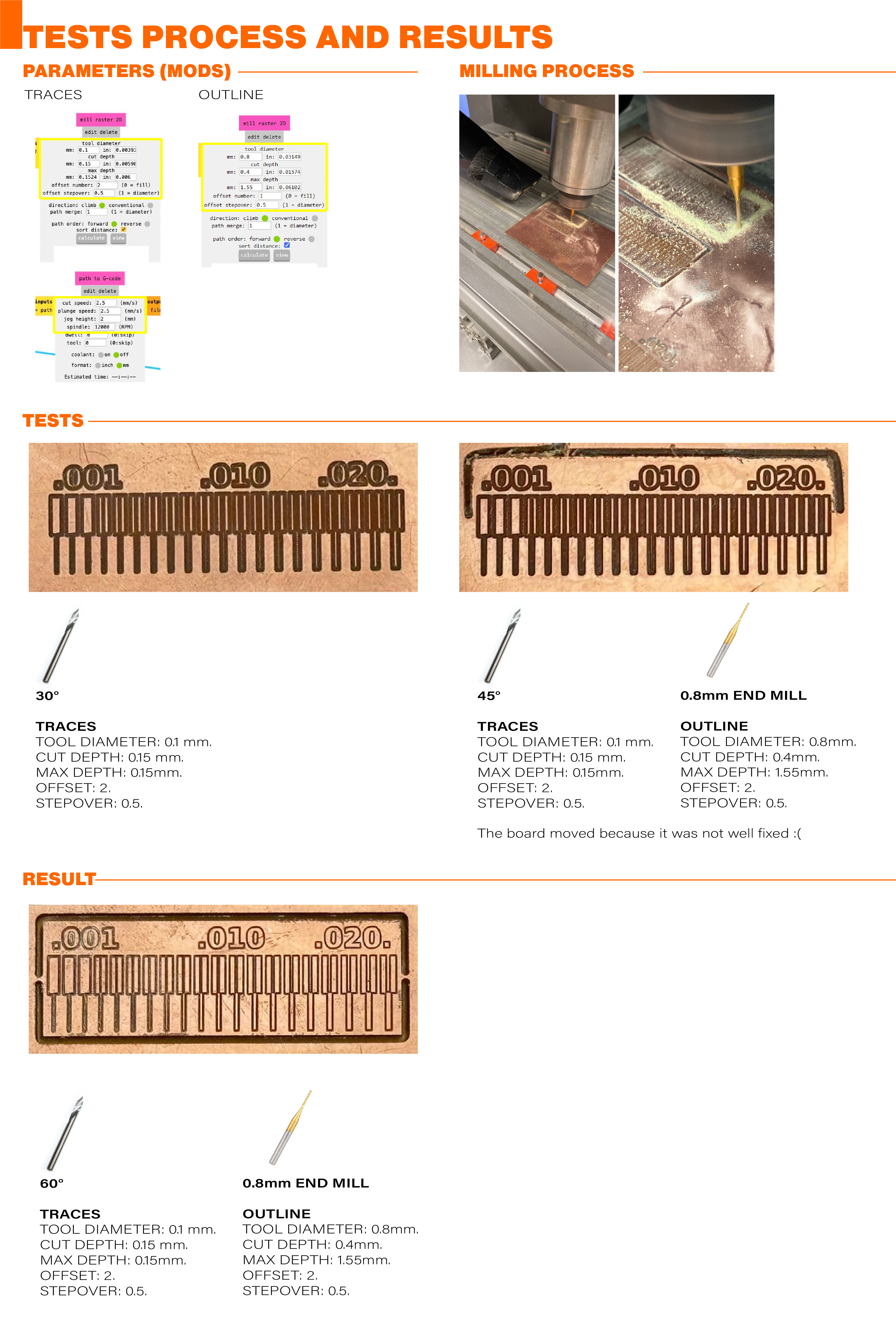
PCB Milling Parameters
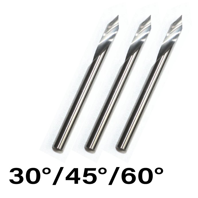
Tool type: 30º / 45º / 60º Angle cutter
| Parameter | MODS PROJECT | FLATCAM | ASPIRE |
|---|---|---|---|
| Spindle Speed | 12000 RPM | 12000 RPM | 12000 RPM |
| Feed Rate | 2.5 mm/s | 2.0 mm/s | 5 mm/s |
| Plunge Rate | 2.5 mm/s | 1.0 mm/s | 1.6 mm/s |
| Pass Depth | 0.4 mm | 0.1 mm | 0.1 mm |
| Stepover (Overlap) | 0.5 | 0.04608 mm | 0.04 mm |
| Stepover (Overlap) % | 50% | 30% | 40% |
| Job Height (Safe Z) | 2 mm | - | 20 mm |
| Tool Diameter | 0.8 mm | 0.1 mm | 0.1 mm |
| Start Depth | - | 0.0 mm | 0.0 mm |
| Cut Depth | 0.4 mm | 0.1 mm | 0.08 mm |
| Max Depth | 1.55 mm | 0.1 mm | - |
| Offset Number | 1 | 0.0 mm | - |
| Passes | - | 4 | 1 |
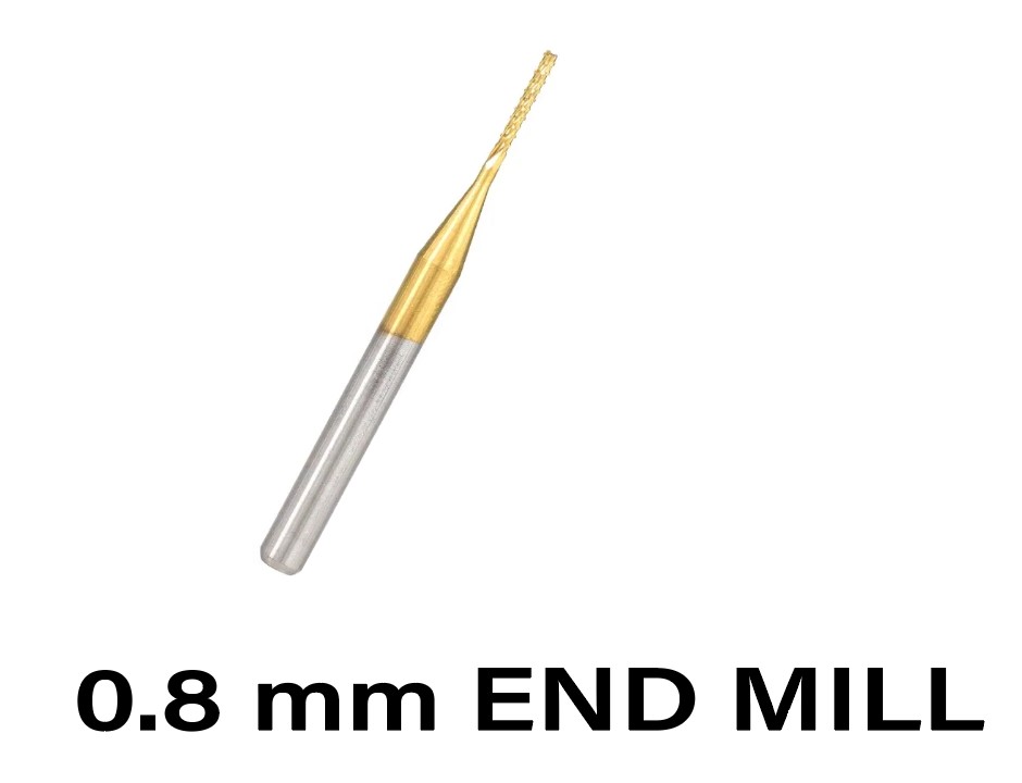
Tool type: 0.8mm Straight end mill
| Parameter | MODS PROJECT | FLATCAM | ASPIRE |
|---|---|---|---|
| Spindle Speed | 12000 RPM | 12000 RPM | 12000 RPM |
| Feed Rate | 2.5 mm/s | 1.4 mm/s | 5 mm/s |
| Plunge Rate | 2.5 mm/s | 1 mm/s | 1.6 mm/s |
| Pass Depth | 0.4 mm | 1.5 mm | 0.8 mm |
| Multi-Depth | - | 0.5 mm (3 passes of 0.5 mm each for a total of 1.5 mm total cut depth) | - |
| Stepover (Overlap) | 0.5 mm | 0.0 mm | 0.4 mm |
| Stepover (Overlap) % | 50% | 0% | 50% |
| Job Height (Safe Z) | 2 mm | 1.5 mm | 20 mm |
| Tool Diameter | 0.8 mm | 0.8 mm | 0.8 mm |
| Start Depth | - | 0 mm | 0.0 mm |
| Cut Depth | 0.4 mm | 0 mm | 0.08 mm |
| Max Depth | 1.55 mm | 0 mm | - |
| Offset Number | 1 | 0 mm | - |
| Passes | - | 1 | 1 |
| Tool Diameter | 0.8 mm | 0.8 mm | 0.8 mm |
| Start Depth | - | 0.0 mm | 0.0 mm |
| Cut Depth | 0.4 mm | 0.0 mm | 1.7 mm |
| Max Depth | 1.55 mm | 1.5 mm | - |
| Offset Number | 1 | - | - |
| Passes | - | 3 | - |
Process and result:
Learnings:
- If you're going to use Mods and are working with PNGs, make sure to use the original file to avoid scale issues.
- Ensure that the board is properly leveled before starting the cutting process; you can use a tool to check the bed leveling in two axes.
- Once you secure the board on the cutting platform, ensure that tape is applied across the area where the board will be machined. Otherwise, there's a risk of it moving during cutting.
- When calibrating the Z axis origin, place the end mill in the center of the board, attach the tool sensor, and calibrate the Z axis ensuring you use a part of the tool sensor surface that is free from irregularities.
- Repeat the Z axis calibration every time you change the tool.
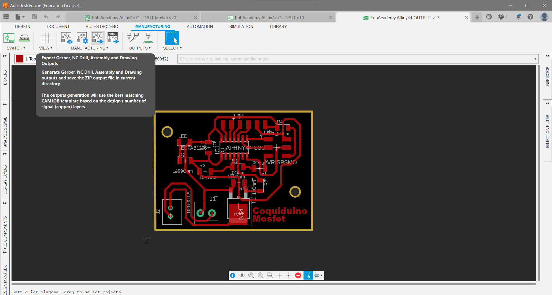
Exporting Fusion 360 GRBL Files
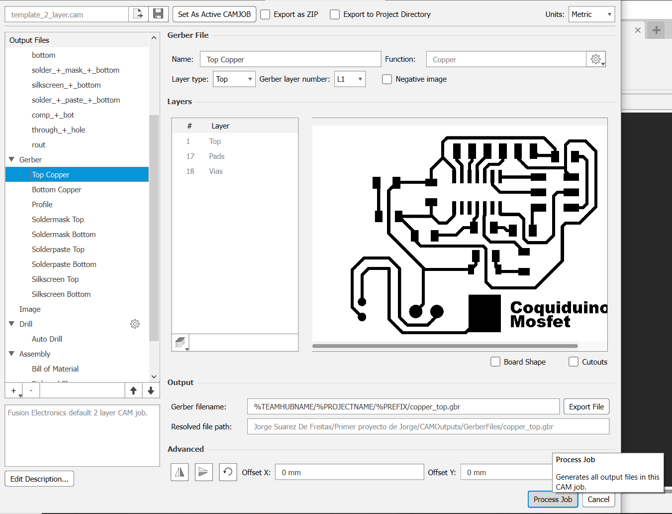
First step is to open the project that you want to send to the PCB House. Then, in Fusion 360, go to the manufacturing tab and export Gerber, NC Drill, Assembly, and Drawing Outputs.
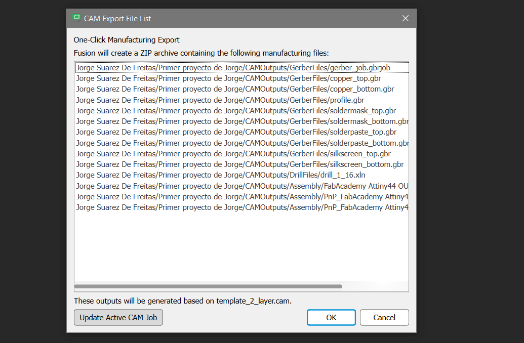
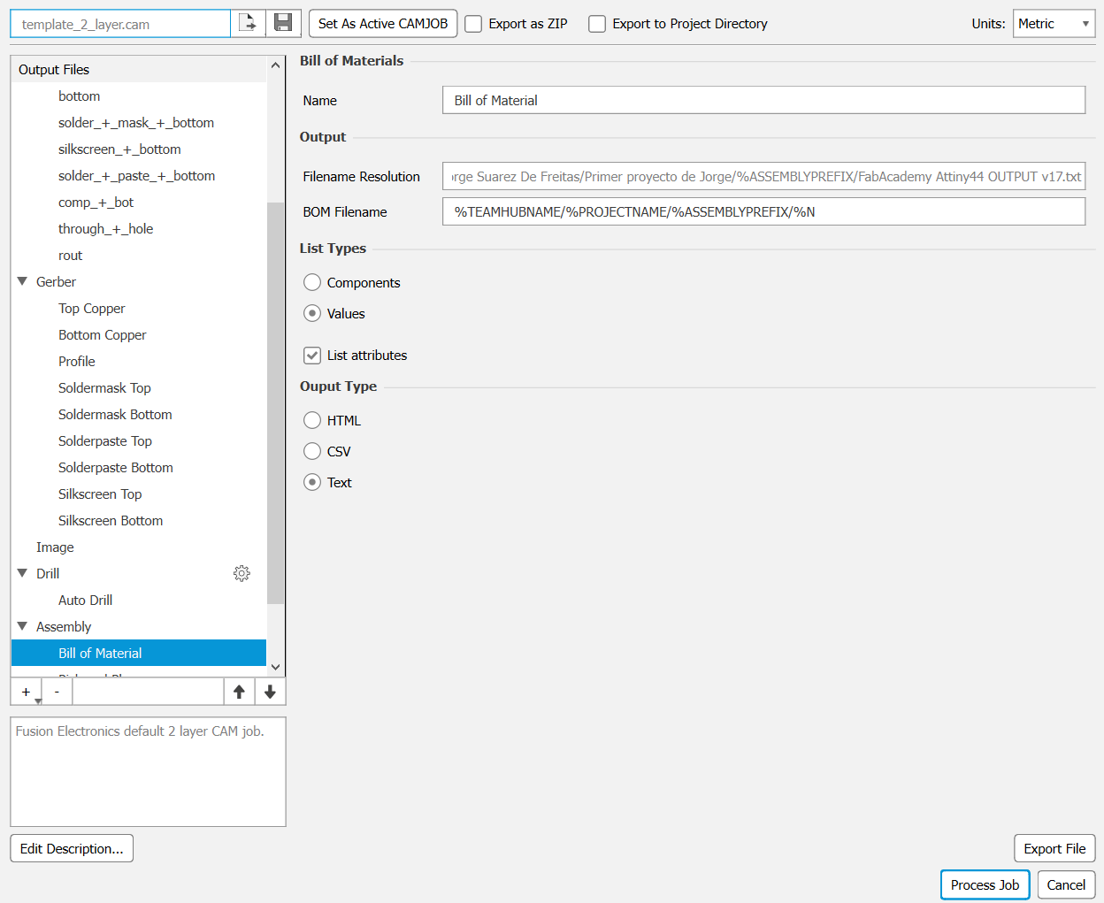
Then this window will pop-up. Here you can select if you want a one-click export that will be created in a zip folder containing all the files. Before exporting, I always check the Gerber Files by clicking on the Update Active CAM Job. A window will pop up showing all the details of the export. Here you can visually check for anything wrong before clicking the Process Job to perform the export.
Documenting the PCB Production Process with JLC PCB
File Preparation
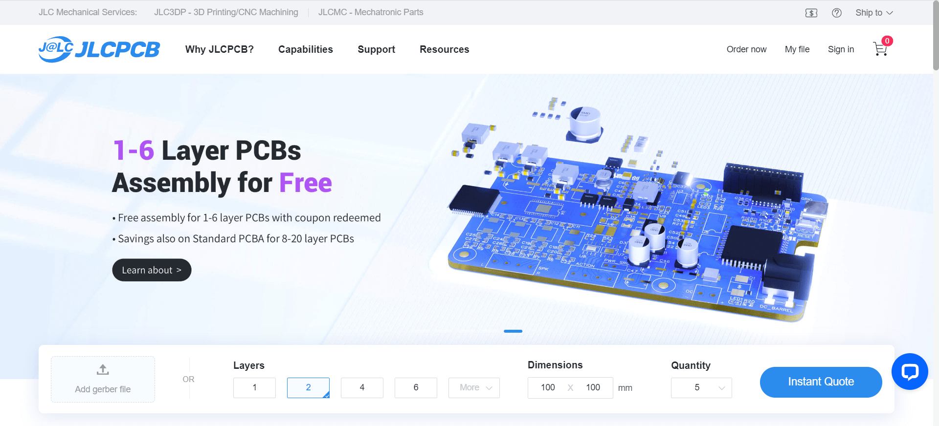
We gathered all necessary Gerber files and related documents required for PCB manufacturing. These files were compressed into a zip folder to ensure they could be easily uploaded to the JLC PCB website.
Material Selection
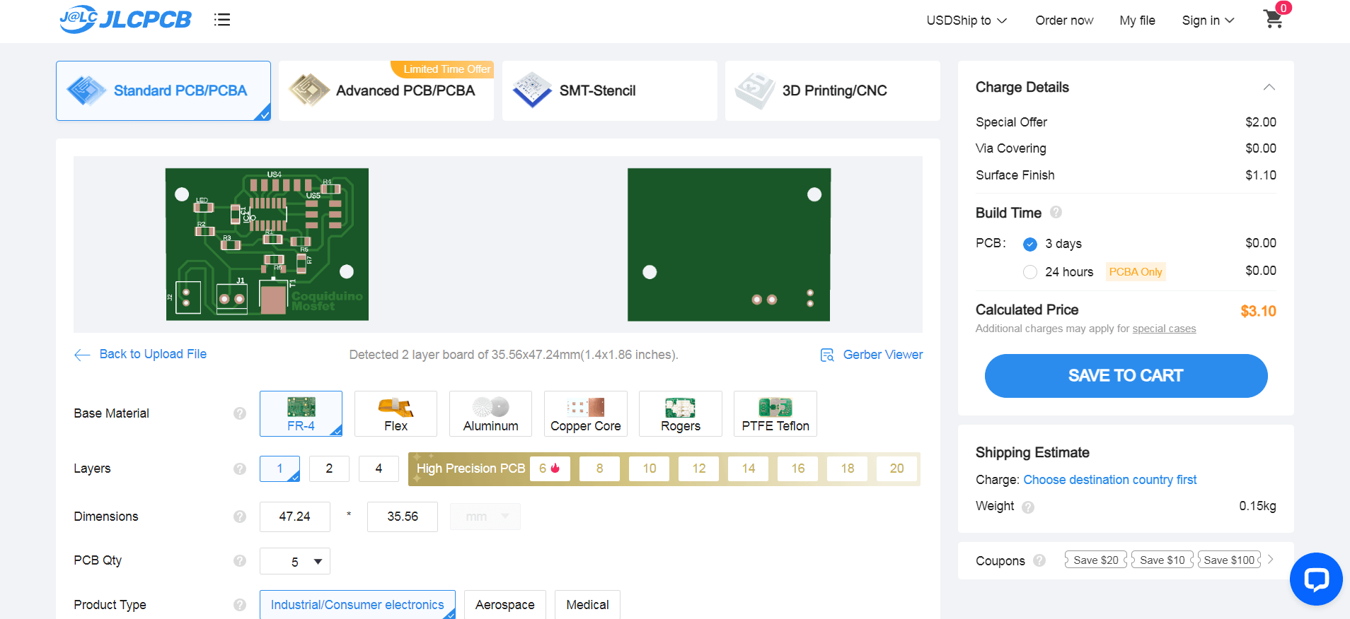
For the PCB material, we chose FR4. This material is widely used for its excellent electrical insulation properties and durability, suitable for a variety of electronic applications.
Layer Configuration
We opted for a 2-layer PCB configuration. This allows flexibility in assembling through-hole components from either the top or bottom of the PCB, depending on design requirements.
Board Dimensions
The dimensions of the PCB were automatically determined from the GRBL files, ensuring precise manufacturing according to the design specifications.
Order Quantity
The minimum order quantity (MOQ) with JLC PCB is 5 units. This quantity meets our project requirements for initial production.
Different Design
Each distinct section of your PCB that is separated by V-cuts, stamp holes, or milling slots typically represents a different design or panelization. Count these sections to determine the number of different designs in your files. In our case, it was 1.
Delivery Format
We selected the delivery format as a single PCB board rather than a panel PCB. This choice is suitable for our current needs and assembly process.
PCB Thickness
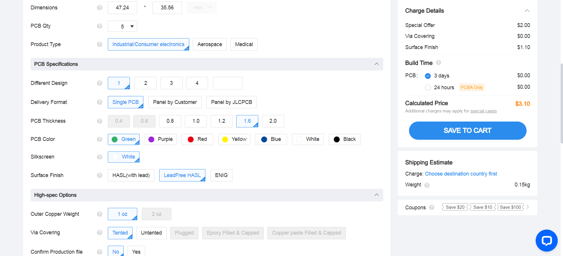
The PCB thickness chosen is 1.6mm. This standard thickness provides robustness and stability to the board structure.
Surface Finish
There were three options available for PCB finish: HASL (Hot Air Solder Leveling), lead-free HASL, and ENIG (Electroless Nickel Immersion Gold). Given the project's requirements for cost-effectiveness and safety, we opted for lead-free HASL. This finish provides adequate protection and solderability without the use of harmful lead.
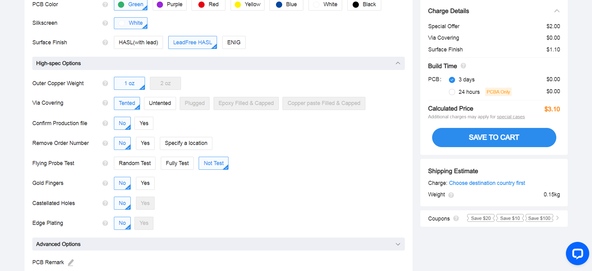
Via Covering
Vias were specified to be tented. Tented vias are covered with solder mask, which helps in preventing solder bridges during assembly, especially for SMD components. This choice ensures a cleaner appearance and smoother soldering process.
Production File Confirmation
We requested confirmation from JLC PCB to verify production files and ensure all details were accurately captured before manufacturing begins.
Quality Control Option
We opted for a Flying Probe Test to test continuity and ensure high-quality production standards.
By carefully selecting these options and configurations, we ensured that the PCB production process with JLC PCB would meet our expectations in terms of quality, functionality, and safety.