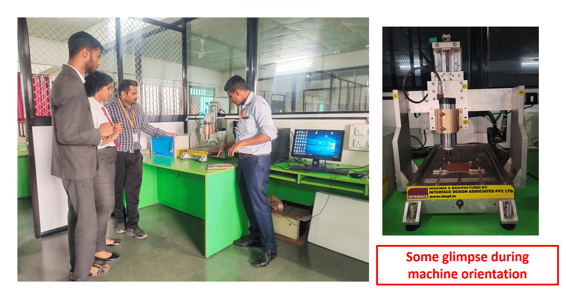
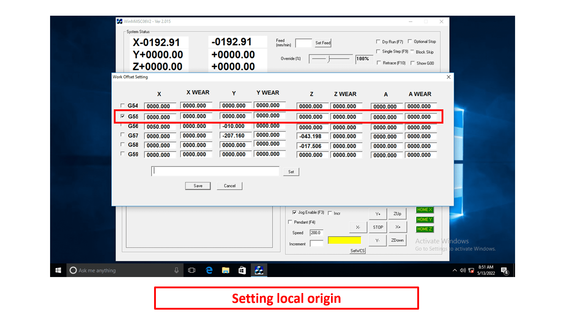
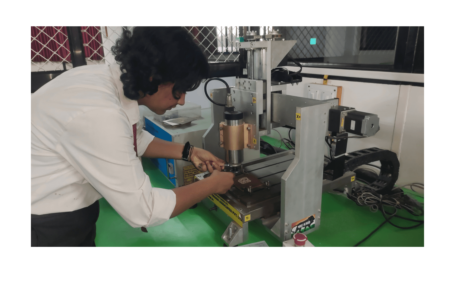
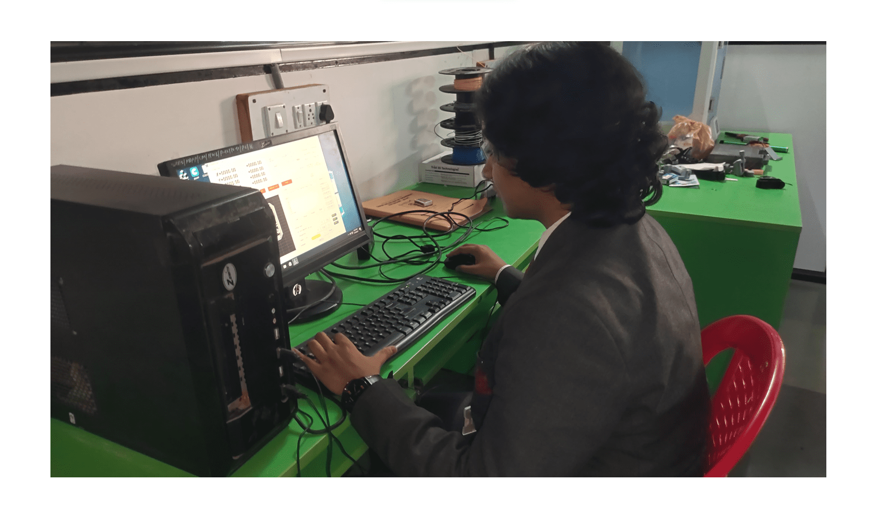
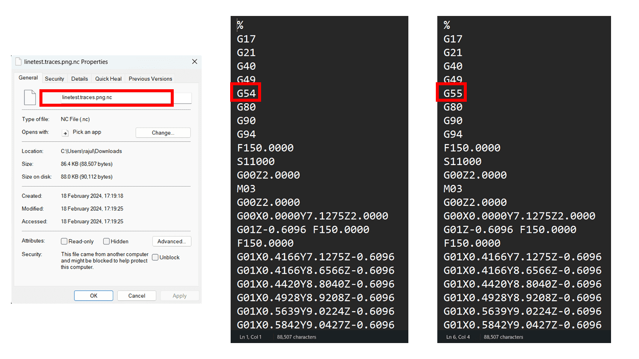
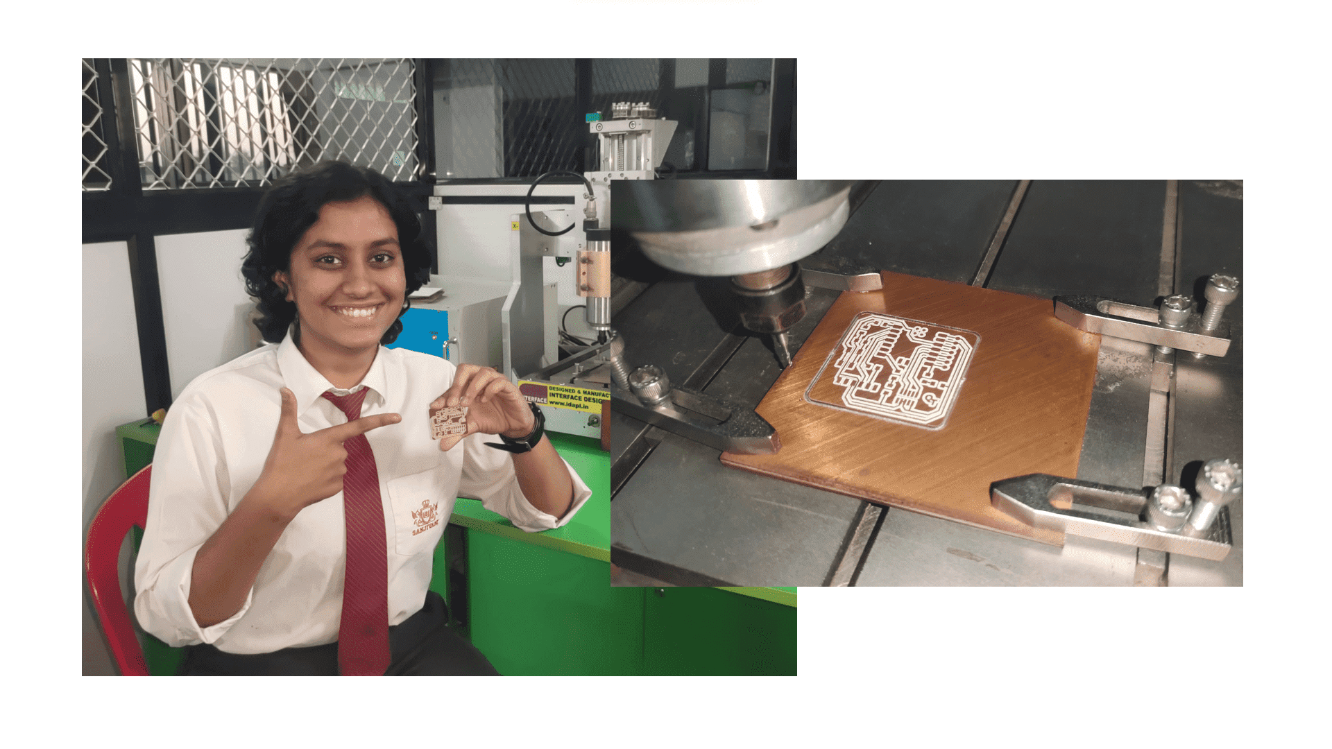
On the second day, Mr. Suhas sir conducted our online lecture to teach us about PCB milling process, conversion of ".png" images of traces and interior of PCB into G-Code using "Modes". After the online lecture my instructor Mr. Kiran sir conducted orientation of PCB Milling Machine physhically. He tought us the operation of PCB Milling software interface, precautions to be taken while operating machine and printing of architecture of PCB.
Before, starting PCB Milling we have to know about some basic concepts are as follows-
A. PCB Fabrication (Process, Material, Machine and Tools)
PCB Fabrication a process of manufacturing PCBs that transforms a circuit board design into a physhical structure based upon the specifications provided in the design package.
1) Etching for PCB Fabrication
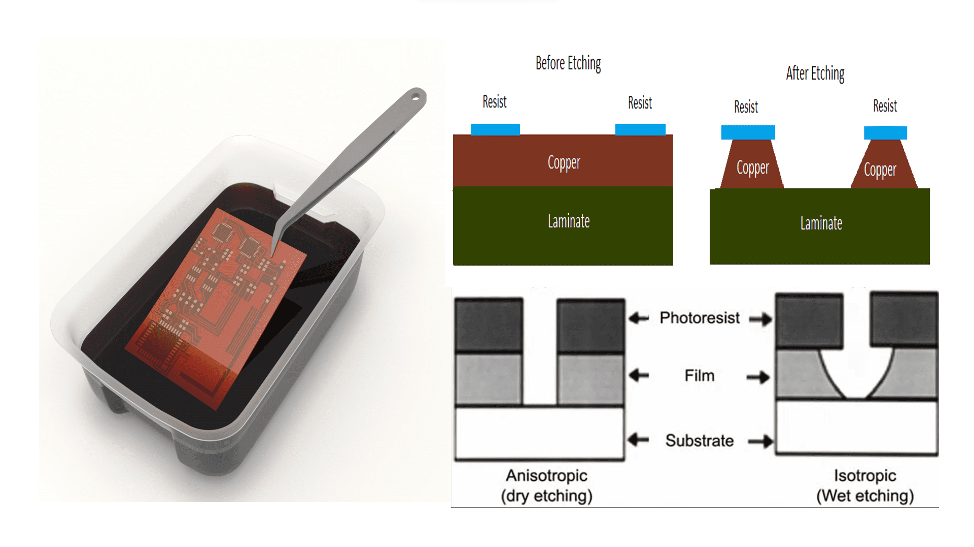
Etching is the process of removing unwanted copper from a printed circuit board. Once all of the excess copper has been removed from the PCB, only the required circuit remains. Before the etching process begins, a layout for the board is generated. This desired layout for the board is transferred onto a PCB by process called photolithography. This forms the blueprint that decides which pieces of copper must be removed from the board.
On the outer layer of PCB, the tin plating acts as the etch resist. However, in the inner layer, the photoresist is the etch resist. Basically,
there are two types of etching are dry etching and wet etching. Dry etching is a process which uses plasma that activates chemical reactions between base and surface atoms of the laminate. This causes the unwanted copper to dissolve. On the other hand, Wet etching is the process uses solution that dissolves unwanted copper using chemical reactions. Depending on the etch material, acidic or alkaline chemical can be used here.
Click here to read more.
Some of the chemicals used in Etching
1. Citric acid = C6H8O7 Sour Salt dry powdered form
2. Acetic acid = CH3COOH (also written as CH3CO2H or C2H4O2) White Vinegar
3. Hydrochloric acid/ Muriatic acid = HCL Swimming Pools to reduce alkalinity
4. Hydrogen Peroxide = H2O2 first aid antiseptic solution, mild disinfectant for wounds
5. Copper sulphate = CuSO4
6. Sodium chloride = NaCl, the chemical name of salt
Precautions to be taken while Etching
1) Wear safety glasses and gloves during etching.
2) Etching can only be done under supervision.
3) Avoid inhalation of vapours.
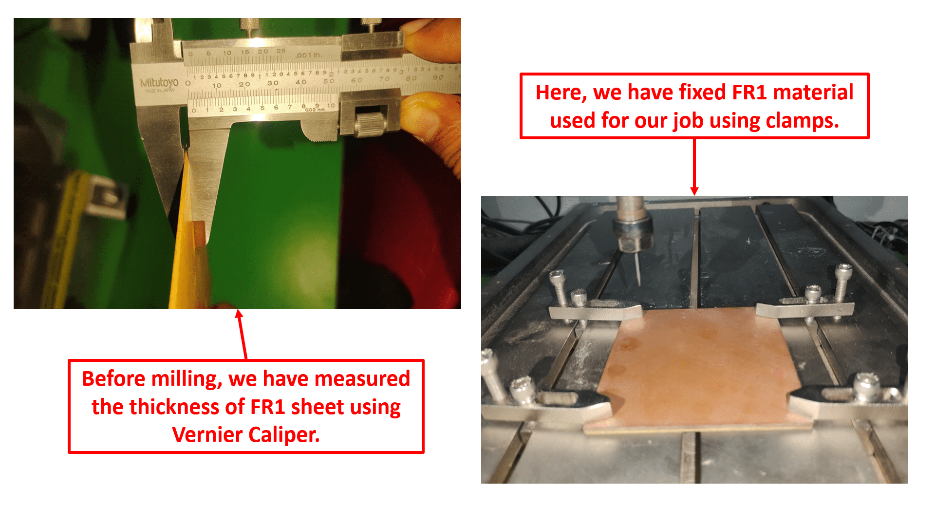
2) Machining (Milling) for PCB Fabrication
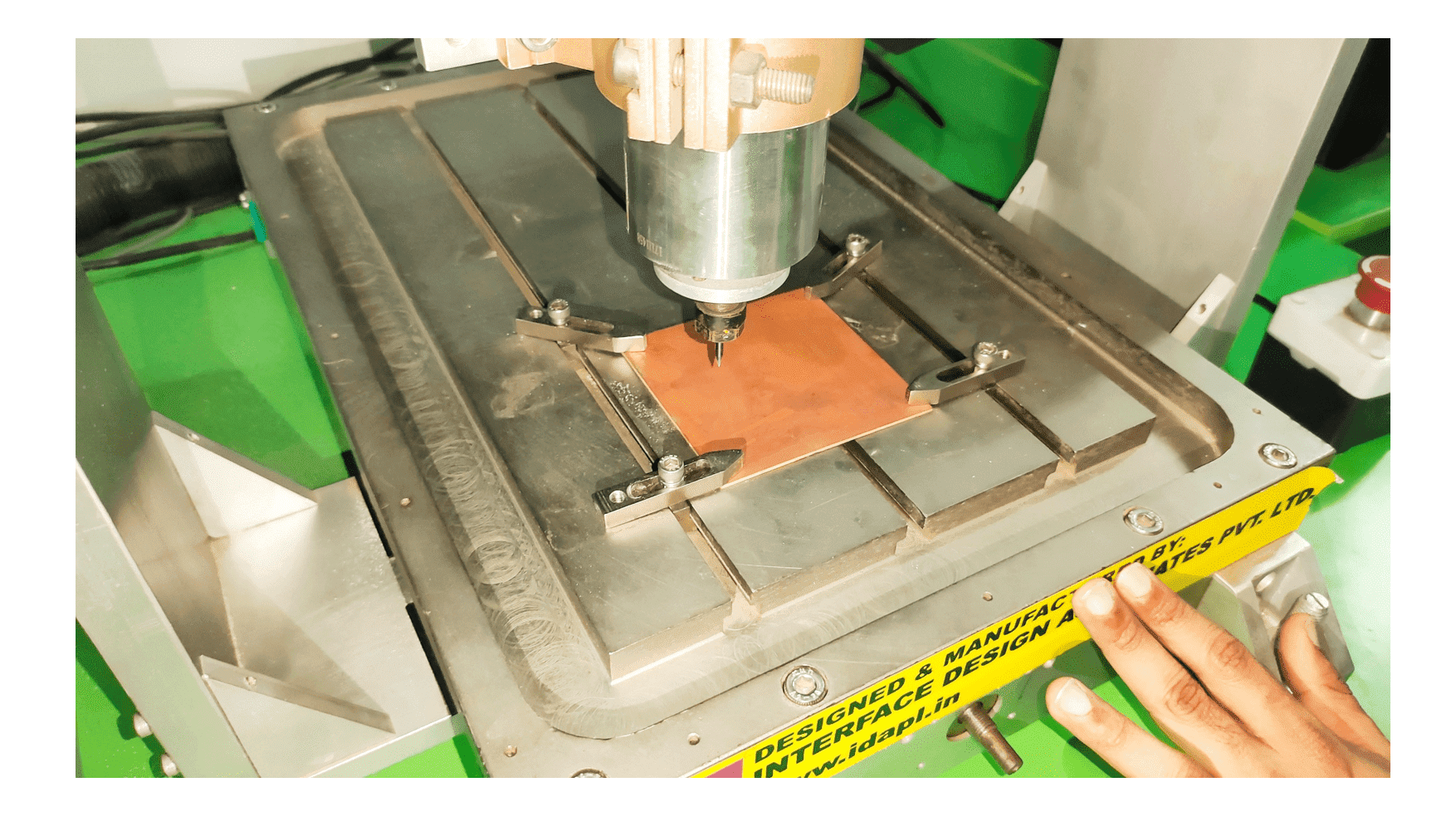
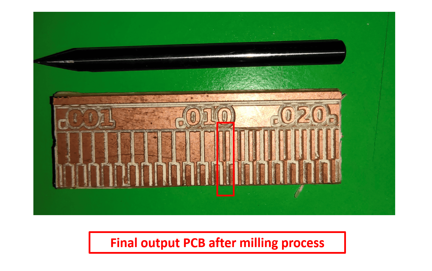
PCB Milling is referred as the process of removing areas of copper from sheet of PCB material to recreate the signal traces, pads as well as structures
based on patterns from a digital circuit board plan called a file of PCB layout.
PCB milling is a non-chemical process, so it can be done in lab environment also. The milling accuracy and sharpness of the milling bits used for milling improves the quality of PCB.
Click here to know more.

Material used in PCB Milling
FR1-Phenolic paper is a type of material used to make printed circuit boards to which components and traces are attached. Basically, it is in brown colour appearance, made up of wood fibre and phenolic polymers. In short, it is a combination of paper and epoxy. Thus, it provides high mechanical strength to the circuit board which makes PCB withstand the load of components.
Machines used in PCB Milling
PCB Milling system is a single machine that can perform all of the required actions to create a prototype board, where components and traces are to be attached.
PCB milling machines are basically roots in "CNC Milling Technology". The CNC Milling is a machining process that utilizes computarized controls to manage the movement and operation of multi-point rotary cutting tools.
Tools used in PCB Milling
Flat end mills tools are mostly used for PCB Milling. Their straigth profiles and consistent diameters gives great clearing large areas of material and it can remove material very quickly.
B. PCB Components and Assembly
There are two types of PCB components are as follows-
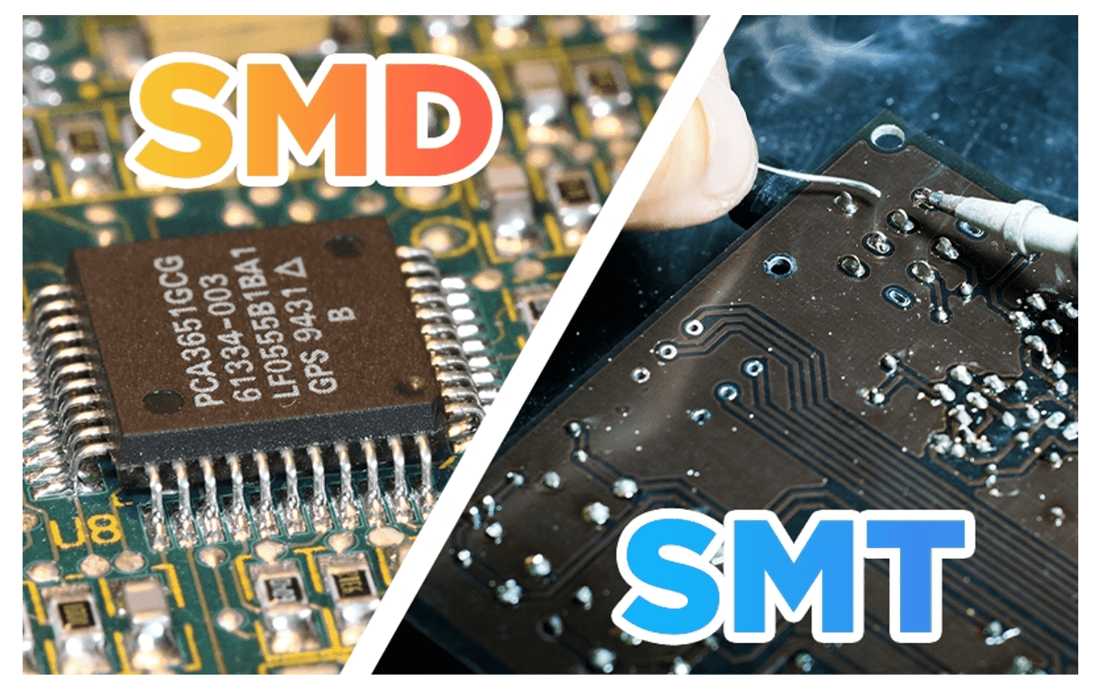
1. Through-hole technology
The name "Through-hole" itself refers that it is manufacturing method in which leads on the components are inserted through holes drilled in printed circuit boards and soldered to pads on the opposite side, either by manual assembly or by use of automated insertation process.
It is the older form of PCB technology which often called as "PTH" (plated through hole) technology. It is the mounting process of mouting on the PCB components throungh plated holes.
2. Surface mount technology
Surface mounting generally called as planar mounting. It is the method in which the electrical components are mounted onto the surface of printed circuit board. Basically, it is component assembly technology used to attach and connect components on the surface of board.
PCB Assembly
A printed circuit board assembly describes the finished board after all the components have been soldered and installed on a printed circuit board.
A circuit board assembler prepares printed circuit boards by soldering electronic components onto them. Reading wiring diagrams, selection of electronic components and finishing boards with hand tools are all includes in PCB assembly.
The first and most commonly used method for assembly is Soldering.
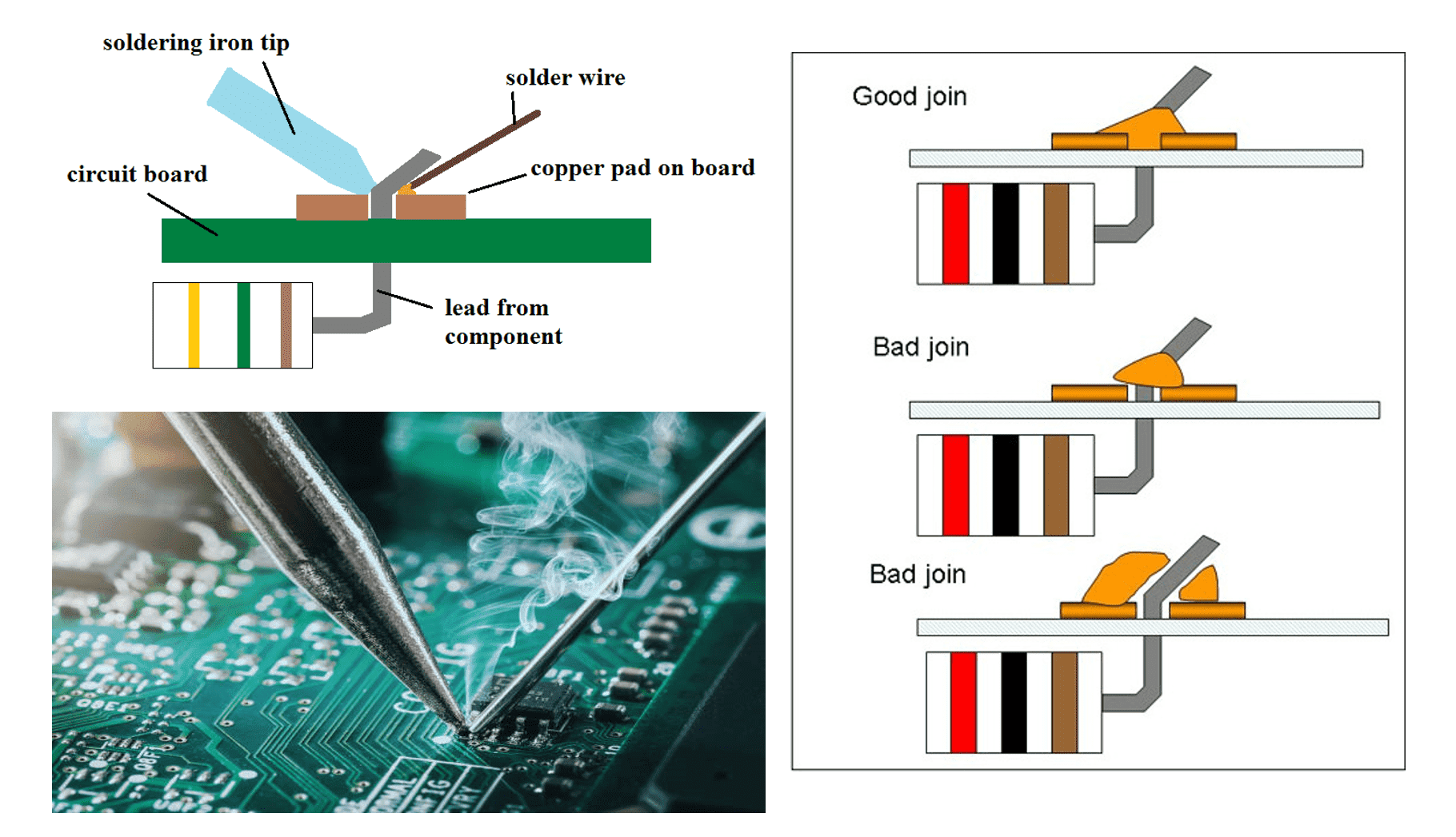
Soldering is a process used for joining metal parts to form mechanical or eletrical bond. Typically, it uses metal alloy having low melting point which is melted and applied to parts to be joined.
Here, the iron is heated to create strong electrical bond.
Solder is a metal alloy used to create a permanent bond between metal workpieces. Solder which is used in making electrical connections also needs to have favourable electrical characteristics.
Click here to know more.
There are different types of solder such as acid core solder, lead alloy solder, flux core solder, rosin core solder, silver alloy solder, etc.
The most commonly used solder is "Tin-Lead solder", which is made up of 60% tin and 40% lead, has 180-190 deg.cel. melting point.

Solder paste is the mixture of the two main elements required to successfully solder together two pieces of metal i.e "powder" and "flux". Solder paste works as an adhesive material while soldering. It also provides electrical and thermal connection.
The most common solder paste powder sizes for surface mount technology are type 3(T3), type 4(T4), type 5(T5). The lower the number, the larger the particle size within the solder powder.
Solder flux is a chemical compound that helps prepare the metal surfaces for soldering by removing oxides and enhancing the flow of solder. The most commonly used solder flux is natural rosin derived from pine tar resin.
Now, the next one process is Desoldering.
The name itself shows that it is the reverse process of soldering. Desoldering is the process of removal of solder and components mounted on circuit boards. The solder joint is removed using the desoldering process. In desoldering process, a small vacuum pump is used to remove solder from the plated through holes. The lead over which the desoldering tip was placed is moved in a circular motion for rounded leads and back and forth for flat leads.
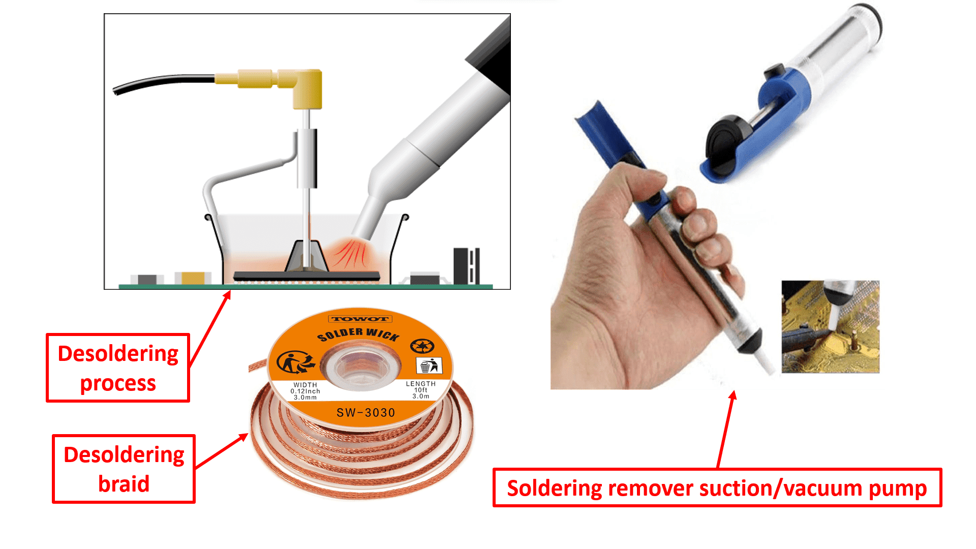
Desoldering braid is pre-fluxed copper braid that is used to remove solder, which allows components to be replaced and excess solder to be removed. It is generally made from oxygen free copper.
Solder remover suction/vacuum pump is a manually-operated device which is used to remove solder from a printed circuit board. firstly you have to heat the solder joint using soldering iron until the solder melts. Then, position the tip of the desoldering pump close to that joint and press the button to activate the vacuum.
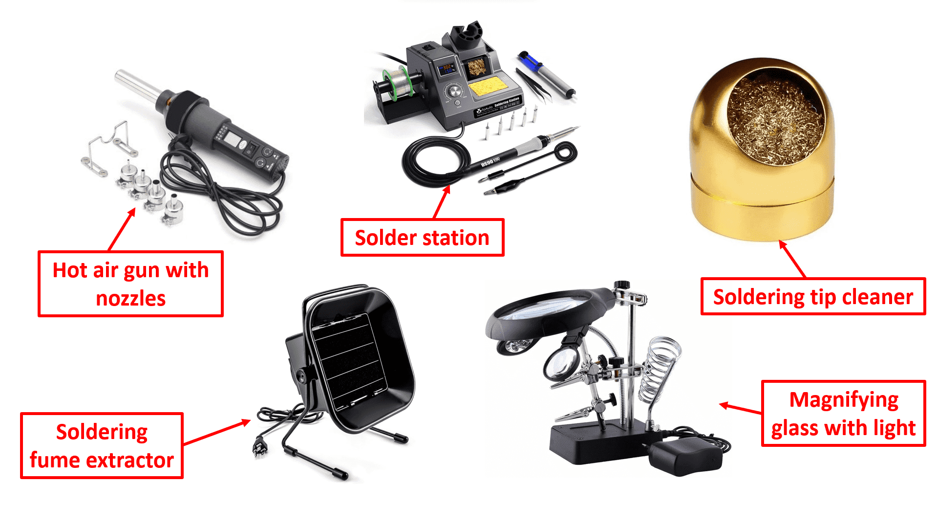
Hot air guns are used to heat up the solder joint, melts the solder and easily remove the components.
Soldering station is used to allows you to adjust the temperature of soldering iron. It help to enhancing the efficiency of soldering process. Soldering stations may include some accessories like holders and stands, soldering tip cleaners, hot air gun, soldering fume extractor and magnifying glass with light, etc.

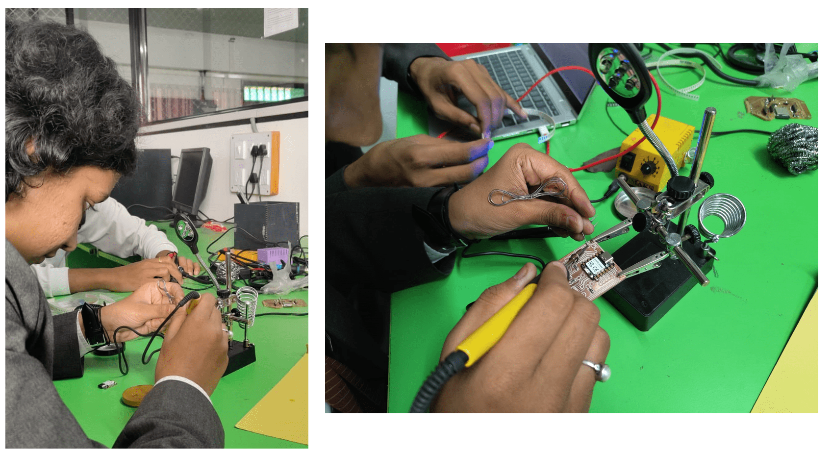
Here is the picture of Soldering station and tools at Sanjivani Fab Lab.